
GaAs SPDT Terminated Switch
DC - 2.5 GHz
SW-337, SW-338, SW-339
V2.00
M/A-COM, Inc.
North America:
Tel. (800) 366-2266
s
Asia/Pacific: Tel. +81 (03) 3226-1671
s
Europe: Tel. +44 (1344) 869 595
Fax (800) 618-8883
Fax +81 (03) 3226-1451
Fax +44 (1344) 300 020
1
Specifications Subject to Change Without Notice.
Electrical Specifications,
T
A
= ±25∞C
Features
Very Low Power Consumption: 75 µW
Low Insertion Loss: 0.5 dB
High Isolation: 33 dB up to 2 GHz (SW-337, SW-338)
28 dB up to 2 GHz (SW-339)
Very High Intercept Point: 46 dBm IP
3
Nanosecond Switching Speed
Temperature Range: -40∞C to +85∞C
Low Cost SOIC8 Plastic Package
Tape and Reel Packaging Available
1
Description
M/A-COM's SW-337, SW-338 and SW-339 are GaAs MMIC
SPDT terminated switches in a low cost SOIC 8-lead
surface mount plastic package. They are ideally suited for
use where very low power consumption is required.
Typical applications include transmit/receive switching,
switch matrices, and filter banks in systems such as: radio
and cellular equipment, PCM, GPS, fiber optic modules,
and other battery powered radio equipment. The difference
between the switches is in the pin configuration.
The SW-337, SW-338 and SW-339 are fabricated with
monolithic GaAs MMICs using a mature 1-micron process.
The process features full chip passivation for increased
performance and reliability.
SO-8
0∞-8∞
.0075-0.0098
(0.19-0.25)
.1890-.1968
(4.80-5.00)
.0099-0.0196
x 45∞ Chamfer
(0.25-0.50)
.2284-.2440
(5.80-6.20)
PIN 8
Orientation
mark
PIN 1
.1497-.1574
(3.80-4.00)
- B -
- A -
.050(1.27) BSC.
.013-.020 TYP.
(0.33-0.51)
.0040-.0098
(0.10-0.25)
- C -
.0532-.0688
(1.35-1.75)
.016-.050
(0.40-1.27)
.010(0.25) M B M
.010(0.25) M C A M B S
.004 (0.10)
Part Number
Package
SW-337 PIN
SOIC 8 Lead
SW-337 TR
Forward Tape & Reel
SW-337 RTR
Reverse Tape & Reel
SW-338 PIN
SOIC 8 Lead
SW-338 TR
Forward Tape & Reel
SW-338 RTR
Reverse Tape & Reel
SW-339 PIN
SOIC 8 Lead
SW-339 TR
Forward Tape & Reel
SW-339 RTR
Reverse Tape & Reel
Ordering Information
SW-337, SW-338
SW-339
Parameter
Test Conditions
2
Unit
Min.
Typ.
Max
Min.
Typ.
Max.
Insertion Loss
DC ≠ 0.1 GHz
dB
0.4
0.6
0.4
0.6
DC ≠ 0.5 GHz
dB
0.5
0.7
0.5
0.7
DC ≠ 1.0 GHz
dB
0.5
0.7
0.5
0.7
DC ≠ 2.0 GHz
dB
0.7
0.9
0.7
0.9
Isolation
DC ≠ 0.1 GHz
dB
50
53
50
53
DC ≠ 0.5 GHz
dB
43
46
43
46
DC ≠ 1.0 GHz
dB
36
39
35
38
DC ≠ 2.0 GHz
dB
30
33
25
28
VSWR
On
DC ≠ 2.0 GHz
1.2:1
1.2:1
Off
DC ≠ 2.0 GHz
1.2:1
1.2:1
Trise, Tfall
10% to 90% RF, 90% to 10% RF
nS
7
7
Ton, Toff
50% Control to 90% RF, 50% Control to 10% RF
nS
10
10
Transients
In Band
mV
25
25
One dB
Input Power
0.05 GHz
dBm
25
25
Compression Point
Input Power
0.5 ≠ 2.0 GHz
dBm
30
30
2nd Order
Measured Relative
0.05 GHz
dBm
60
60
Intercept
to Input Power
0.5 ≠ 2.0 GHz
dBm
65
65
(for two-tone input power up to +5 dBm)
3rd Order
Measured Relative
0.05 GHz
dBm
40
40
Intercept
to Input Power
0.5 ≠ 2.0 GHz
dBm
46
46
(for two-tone input power up to +5 dBm)
1. Refer to "Tape and Reel Packaging" Section, or contact factory.
2. All measurements with 0, -5 control voltages at 1 GHz in a 50
system, unless otherwise specified.
q
q
q
q
q
q
q
q
8-Lead SOP outline dimensions
Narrow body .150
(All dimensions per JEDEC No. MS-012-AA, Issue C)
Dimensions in ( ) are in mm.
Unless otherwise noted: .xxx = ±0.010 (.xx = ±0.25)
.xx = ±0.02 (.x = ±0.5)
GaAs SPDT Terminated Switch
SW-337, SW-338, SW-339
V2.00
M/A-COM, Inc.
North America:
Tel. (800) 366-2266
s
Asia/Pacific: Tel. +81 (03) 3226-1671
s
Europe: Tel. +44 (1344) 869 595
Fax (800) 618-8883
Fax +81 (03) 3226-1451
Fax +44 (1344) 300 020
2
Specifications Subject to Change Without Notice.
Parameter
Absolute Maximum
1
Max. Input Power
0.05 GHz
+27 dBm
0.5 ≠ 2.0 GHz
+34 dBm
Control Voltage
+5V, -8.5V
Operating Temperature
-40∞C to +85∞C
Storage Temperature
-65∞C to +150∞C
Absolute Maximum Ratings
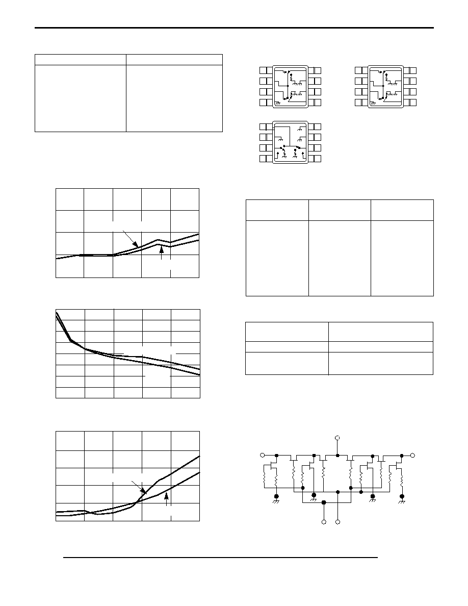
Pin Configuration
SW-337
SW-338
SW-339
Truth Table
Typical Performance
@ +25∞C
1. Operation of this device above any one of these parameters may
cause permanent damage.
8
7
6
5
1
4
3
2
RF1
GND
GND
RFC
GND
RF2
B
A
8
7
6
5
1
4
3
2
RF1
GND
GND
RFC
GND
RF2
A
B
5
4
A
B
6
3
RF1
RF2
7
2
GND
GND
RFC
GND
8
1
RF1
RF COM
Q1
Q2
Q3
Q4
RF2
A
B
Q6
Q5
Q8
Q7
T1
G1
G2
T2
FREQUENCY (GHz)
2.0
1.5
1.0
0.5
0
0
0.5
1.0
1.5
2.0
2.5
LOSS (dB)
ISOLATION vs FREQUENCY
VSWR vs FREQUENCY
INSERTION LOSS vs FREQUENCY
SW-337, SW-338
SW-339
FREQUENCY (GHz)
2.0
1.8
1.6
1.4
1.2
1.0
0
0.5
1.0
1.5
2.0
2.5
VSWR
RCF, RF1, RF2 On
RF1, RF2 Off
80
70
60
50
40
30
20
10
0
0
0.5
1.0
1.5
2.0
2.5
FREQUENCY (MHz)
ISOLATION (dB)
Pin Pin Pin
No. Description
No. Description
No. Description
1
A
1
B
1
RF Common
2
RF Common
2
RF Common
2
GND
3
B
3
A
3
RF1
4
GND
4
GND
4
A
5
RF1
5
RF1
5
B
6
GND
6
GND
6
RF2
7
GND
7
GND
7
GND
8
RF2
8
RF2
8
GND
Condition of Switch
Control Inputs
RF Common to Each RF Port
A
B
RF1
RF2
1
0
ON
OFF
0
1
OFF
ON
"0" ≠ 0 ≠ -0.2V @ 20 µA max.
"1" ≠ -5V @ 30 µA Typ to -8V @ 720 µA max.
SW-337, SW-338
SW-339
Functional Schematics
Electrical Schematic
SW-339
SW-337
SW-338