GaAs High Isolation Switch, DC - 3.0 GHz
SW-439
M/A-COM Division of AMP Incorporated
3
North America: Tel. (800) 366-2266, Fax (800) 618-8883
3
Asia/Pacific: Tel.+81 44 844 8296, Fax +81 44 844 8298
3
Europe: Tel. +44 (1344) 869 595, Fax+44 (1344) 300 020
www.macom.com
AMP and Connecting at a Higher Level are trademarks.
The Preliminary Specificatons Data Sheet contains typical specifications which may change prior to the final introduction.
V2.00
Features
∑
Low Power Consumption: < 15 µA @ +2.5V
∑
High Isolation: 50 dB Typical @ 2 GHz
∑
Low Insertion Loss: < 0.8 dB @ 2 GHz
∑
Positive 2.5 to 5 V Control
∑
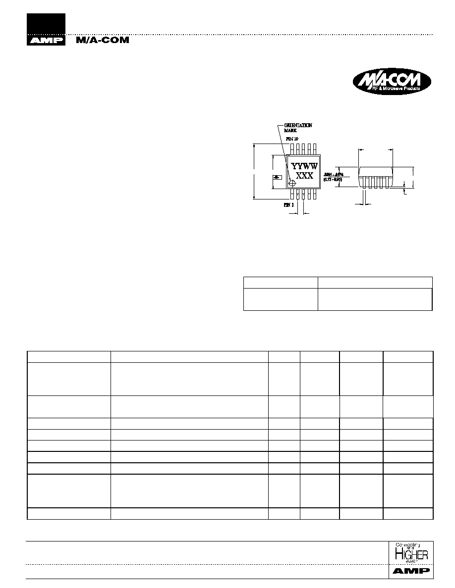
Low Cost Plastic MSOP-10 Package
MSOP-10
Electrical Specifications: T
A
= +25∞C
GaAs High Isolation Switch
DC - 3.0 GHz
SW-439
Description
M/A-COM's SW-439 is a GaAs MMIC SPDT switch in a low
cost MSOP-10 surface mount plastic package. This part is ideal
for high isolation, broadband switching requirements. Typical
applications include synthesizer switching, transmit/receive
switching, switch matrices and filter banks in systems such as
radio and cellular equipment, PCM, GPS, and fiber optic mod-
ules
The SW-439 is fabricated as a monolithic GaAs MMIC using a
mature 1 micron process. The process features full passivation
Ordering Information
Part Number
Package
SW-439 PIN
MSOP 10-Lead Plastic Package
SW-439TR
Tape and Reel
Parameter
Test Conditions
Units
Min.
Typ.
Max.
Insertion Loss
DC - 1.0 GHz
dB
0.55
0.65
1.0 - 2.0 GHz
dB
0.65
0.75
2.0 - 3.0 GHz
dB
0.80
0.90
Isolation
DC - 2.0 GHz
dB
45
47
2.0 - 3.0 GHz
dB
31
33
VSWR
0.25 - 3.0 GHz
1.2:1
1.3:1
P
1dB
(2.5V supply)
500 MHz - 2.0 GHz
dBm
20
P
1dB
(5V supply)
500 MHz - 2.0 GHz
dBm
28
IP
2
2 Tone 900 MHz, 5 MHz Spacing (2.5 V)
dBm
85
IP
3
2 Tone 900 MHz, 5 MHz Spacing (2.5 V)
dBm
50
T
on
, T
off
50% Control to 90% RF, Control to 10% RF
ns
20
T
rise
, T
fall
10% to 90% RF, 90% to 10% RF
ns
10
Transients
In-band
mV
15
Gate Leakage
|V
CTL
| = 2.5 V
µA
5
15
.0197
BSC.
.1142 - .1220
.1929
BSC
.1142 - .1220
.0059 - .0118
.0020 - .0059
.0433
MAX

GaAs High Isolation Switch, DC - 3.0 GHz
SW-439
M/A-COM Division of AMP Incorporated
3
North America: Tel. (800) 366-2266, Fax (800) 618-8883
3
Asia/Pacific: Tel.+81 44 844 8296, Fax +81 44 844 8298
3
Europe: Tel. +44 (1344) 869 595, Fax+44 (1344) 300 020
www.macom.com
AMP and Connecting at a Higher Level are trademarks.
The Preliminary Specificatons Data Sheet contains typical specifications which may change prior to the final introduction.
V2.00
1
1.1
1.2
1.3
1.4
1.5
1.6
1.7
1.8
1.9
2
0
0.5
1
1.5
2
2.5
3
FREQUENCY (GHz)
IL (dB)
-40∞C
+25∞C
+85∞C
30
35
40
45
50
55
60
65
70
0
0.5
1
1.5
2
2.5
3
FREQUENCY (GHz)
IL (dB)
+25∞C
-40∞C
+85∞C
0
0.1
0.2
0.3
0.4
0.5
0.6
0.7
0.8
0.9
1
0
0.5
1
1.5
2
2.5
3
FREQUENCY (GHz)
IL (dB)
+85∞C
+25∞C
-40∞C
Typical Performance Curves
Functional Schematic
1
Parameter
Absolute Maximum
Input Power
+30 dBm
Operating Voltage
+8.5 Volts
Operating Temperature
-40∞C to +85∞C
Storage Temperature
-65∞C to +150∞C
Absolute Maximum Ratings
1
1.
Exceeding any one or a combination of these limits may cause
permanent damage.
1.
External blocking capacitors are required on all RF ports.
Insertion Loss vs. Frequency Over
Temperature
Isolation vs. Frequency Over Temperature
VSWR vs. Frequency Over Temperature
Mode
(Control)
Control
1
V1
Control
2
V2
RFC - RF1
RFC - RF2
Positive
1
0V
+2.5 to +5V
Off
On
+2.5 to +5V
0V
On
Off
1.
External DC blocking capacitors are required on all RF ports.
2.
Logic 0=0±0.2 Vdc Logic 1 = +2.5 to +5 Vdc
Truth Table
PIN No.
Function
Description
1
V1
Control 1
2
Gnd
Ground
3
RFC
RF Input
4
Gnd
Ground
5
V2
Control 2
6
RF2
RF Port 2
7
Gnd
Ground
8
Gnd
Ground
9
Gnd
Ground
10
RF1
RF Port 1
Pin Configuration
Pin 1
V1 Gnd RFC Gnd V2
RF1 Gnd Gnd Gnd RF2
C=39pF
C=39pF
C=39pF
Pin 10