ADVANCED INFORMATION
2V Control Triple-Band GSM/DCS/PCS SP5T Switch SW-444
0.5 ≠ 2.0 GHz
Rev 1.4
The Advanced Information Data Sheet Contains Typical Electrical Specifications Which May Change Prior to Final Introduction
.
M/A-COM, Inc.
1
North America: Tel. (800) 366-2266
Asia/Pacific: Tel. +81 3 3263-8761
Europe:
Tel. +44 (1344) 869-595
Fax (800) 618-8883 Fax +81 3 3263-8769
Fax +44 (1344) 300-020
Features
∑
GSM Power Handling with +2.0V Control
Voltage
∑
Low Power Consumption. Less than 1
µ
A in Rx
mode
∑
Integrated Decoder
∑
Leadless 4 x 4 mm FQFP-N, 20 Pin Package
∑
Low Insertion Loss of 0.6 dB in GSM Transmit
Mode
Description
The M/A-COM SW-444 is a GaAs monolithic
switch in a low cost, FQFP-N, surface mount plastic
package. The SW-444 is ideally suited for
applications where very low power consumption,
high power handling, and low cost are required. The
SW-444 includes an integrated decoder. This switch
is designed for Transmit and Receive switching for
Triple-Band GSM/DCS/PCS Mobile Phones. The
switch offers GSM power handling as low as +2.0
V control voltage. The supply voltage VDD should
be connected to the highest available voltage and
may be unregulated.
The SW-444 is fabricated using a new 0.5-micron
gate length GaAs pHEMT process. The process
features full chip passivation for increased
performance and reliability.
.
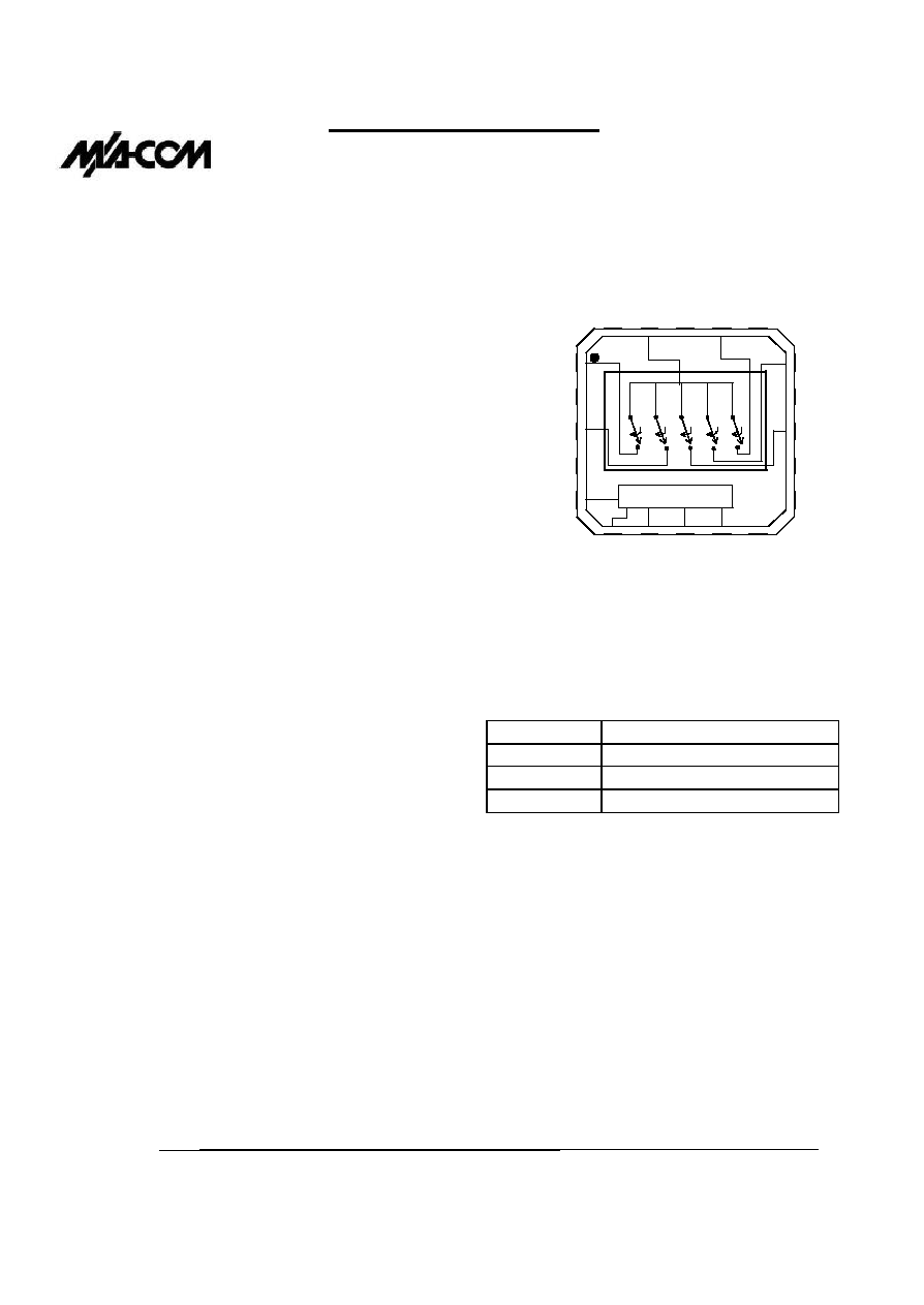
Functional Schematic
Ordering Information
Part Number
Description
SW-444TR
SW-444 on 1000 Piece Tape and Reel
SW-444TR-3000
SW-444 on 3000 Piece Tape and Reel
SW-444SMB
SW-444 Sample Test Board
Decoder
GND
ANT
GND
GRX
PRXS
PTX/DTX
GND
GTX
GND
VDD
BS
TXS
PRXON
GND
PRX
DRXS
DRX
GND
GND
GND
2V Control Triple-Band GSM/DCS/PCS SP5T Switch
SW-444
V1.4
The Advanced Information Data Sheet Contains Typical Electrical Specifications Which May Change Prior to Final Introduction
.
M/A-COM, Inc.
2
North America: Tel. (800) 366-2266
Asia/Pacific: Tel. +81 3 3263-8761
Europe:
Tel. +44 (1344) 869-595
Fax (800) 618-8883 Fax +81 3 3263-8769
Fax +44 (1344) 300-020
ELECTRICAL CHARACTERISTICS:
Test Conditions: VDD = 2.5V, Vctrl =2.0V, T
A
= +25
∞
C
Mode
Specifications
Freq. (MHz)
Units
Min.
Typ.
Max.
ANT -> GSM RX
Insertion Loss
925 - 960
dB
0.74
0.8
0.9
Isolation GSM Tx to ANT
Isolation GSM Tx to GSM Rx
Isolation GSM Tx to PCS Rx
Isolation GSM Tx to DCS Rx
Isolation PCS/DCS Tx to ANT
Isolation PCS/DCS Tx to GSM Rx
Isolation PCS/DCS Tx to PCS Rx
Isolation PCS/DCS Tx to DCS Rx
880 - 915
880 - 915
880 - 915
880 - 915
1710 - 1785
1710 - 1785
1710 - 1785
1710 - 1785
dB
dB
dB
dB
dB
dB
dB
dB
25
26
32
32
22
23
32
32
27
28
>35
>35
24
25
>35
>35
30
30
52
64
26
27
43
54
ANT -> PCS RX
Insertion Loss
1930 - 1990
dB
0.94
1.0
1.1
Isolation GSM Tx to ANT
Isolation GSM Tx to GSM Rx
Isolation GSM Tx to PCS Rx
Isolation GSM Tx to DCS Rx
Isolation PCS/DCS Tx to ANT
Isolation PCS/DCS Tx to GSM Rx
Isolation PCS/DCS Tx to PCS Rx
Isolation PCS/DCS Tx to DCS Rx
880 - 915
880 - 915
880 - 915
880 - 915
1710 - 1785
1710 - 1785
1710 - 1785
1710 - 1785
dB
dB
dB
dB
dB
dB
dB
dB
25
32
26
32
22
32
23
32
27
>35
28
>35
24
>35
25
>35
29
55
30
52
26
42
27
42
ANT -> DCS RX
Insertion Loss
1805 - 1880
dB
0.94
1.0
1.1
Isolation GSM Tx to ANT
Isolation GSM Tx to GSM Rx
Isolation GSM Tx to PCS Rx
Isolation GSM Tx to DCS Rx
Isolation PCS/DCS Tx to ANT
Isolation PCS/DCS Tx to GSM Rx
Isolation PCS/DCS Tx to PCS Rx
Isolation PCS/DCS Tx to DCS Rx
880 - 915
880 - 915
880 - 915
880 - 915
1710 - 1785
1710 - 1785
1710 - 1785
1710 - 1785
dB
dB
dB
dB
dB
dB
dB
dB
25
32
32
26
22
32
32
23
27
>35
>35
28
24
>35
>35
25
29
56
60
30
26
44
51
27
ANT -> GSM TX
Insertion Loss
880 - 915
dB
0.54
0.6
0.7
Isolation GSM Tx to GSM Rx
Isolation GSM Tx to PCS Rx
Isolation GSM Tx to DCS Rx
Isolation PCS/DCS Tx to ANT
Isolation PCS/DCS Tx to GSM Rx
Isolation PCS/DCS Tx to PCS Rx
Isolation PCS/DCS Tx to DCS Rx
880 - 915
880 - 915
880 - 915
1710 - 1785
1710 - 1785
1710 - 1785
1710 - 1785
dB
dB
dB
dB
dB
dB
dB
29
31
32
22
32
32
32
31
33
34
24
>35
>35
>35
33
35
36
26
44
59
59
ANT -> PCS/DCS TX
Insertion Loss
1710 - 1785
dB
0.84
0.9
1.0
Isolation GSM Tx to ANT
Isolation GSM Tx to GSM Rx
Isolation GSM Tx to PCS Rx
Isolation GSM Tx to DCS Rx
Isolation PCS/DCS Tx to GSM Rx
Isolation PCS/DCS Tx to PCS Rx
Isolation PCS/DCS Tx to DCS Rx
880 - 915
880 - 915
880 - 915
880 - 915
1710 - 1785
1710 - 1785
1710 - 1785
dB
dB
dB
dB
dB
dB
dB
25
32
32
32
23
32
31
27
>35
>35
>35
25
34
33
29
55
60
64
27
36
35
ANT/PRX/DRX/GRX -> GND
(IDLE MODE)
Isolation GSM Tx to ANT , FREQ = 900 MHz
Isolation PCS/DCS Tx to ANT , FREQ = 1810 MHz
925 ≠ 960
925 - 960
dB
dB
34
34
34
34
34
34
2nd Harmonics
Freq = 900 MHz, Input Power = +34 dBm
Freq = 1810 MHz, Input Power = +32 dBm
dBc
dBc
-84
-84
-79
-79
-70
-65
3rd Harmonics
Freq = 900 MHz, Input Power = +34 dBm
Freq = 1810 MHz, Input Power = +32 dBm
dBc
dBc
-73
-73
-69
-69
-65
-65
Supply Voltage
Volts
2.0
2.5
4.0
High Control Voltages
Volts
2.0
2.5
4.0
Low Control Voltages
Volts
-0.2
0
0.2
1.
DC blocking capacitors are required on all RF and shunt ports.
2.
All impedances are 50 ohms.
2V Control Triple-Band GSM/DCS/PCS SP5T Switch
SW-444
V1.4
The Advanced Information Data Sheet Contains Typical Electrical Specifications Which May Change Prior to Final Introduction
.
M/A-COM, Inc.
4
North America: Tel. (800) 366-2266
Asia/Pacific: Tel. +81 3 3263-8761
Europe:
Tel. +44 (1344) 869-595
Fax (800) 618-8883 Fax +81 3 3263-8769
Fax +44 (1344) 300-020
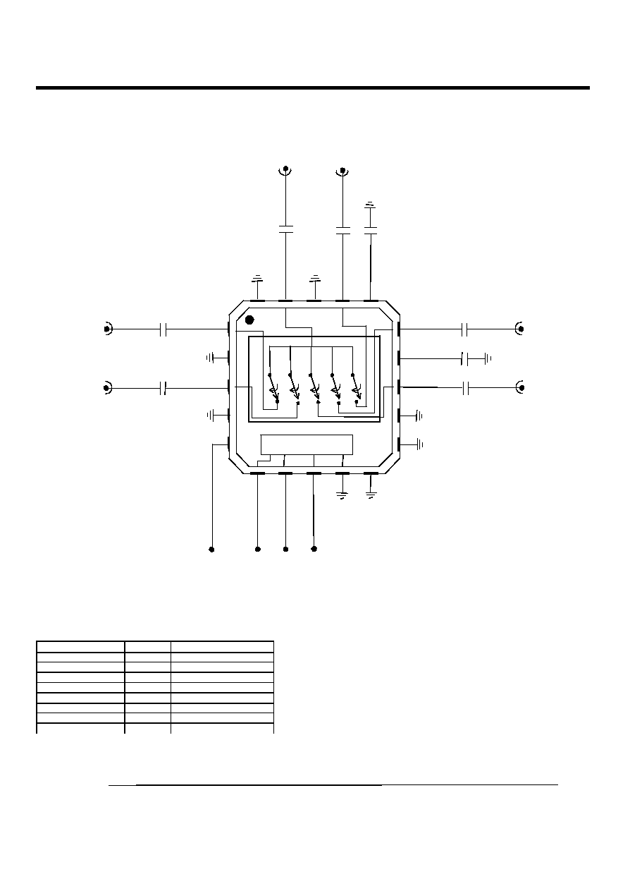
Sample Board Schematic
External Circuitry Parts List (Note: Values of external elements not final)
Ref. Designation
Value
Purpose
C1
22pF
DC Block
C2
22pF
DC Block
C3
22pF
DC Block
C4
4.7pF
RF Shunt
C5
22pF
DC Block
C6
4.7pF
RF Shunt
C7
22pF
DC Block
C8
22pF
DC Block
VDD
TXS
PRXON
PTX/DTX
GTX
PRX
DRX
ANT
GRX
C1
C2
C3
C4
C5
C7
C8
BS
C6
Decoder

2V Control Triple-Band GSM/DCS/PCS SP5T Switch
SW-444
V1.4
The Advanced Information Data Sheet Contains Typical Electrical Specifications Which May Change Prior to Final Introduction
.
M/A-COM, Inc.
5
North America: Tel. (800) 366-2266
Asia/Pacific: Tel. +81 3 3263-8761
Europe:
Tel. +44 (1344) 869-595
Fax (800) 618-8883 Fax +81 3 3263-8769
Fax +44 (1344) 300-020
4 mm FQFP-N, 20-Lead
Measurement (mm)
Dimension
Min.
Nom.
Max.
A
A1
A2
A3
b
D
D1
D2
e
E
E1
E2
L
0.80
0
0
0.18
0.75
0.75
0.35
0.90
0.02
0.65
0.25 ref.
0.23
4.00 basic
3.75 basic
1.70
0.50 basic
4.00 basic
3.75 basic
1.70
0.55
1.00
0.05
1.00
0.30
2.25
2.25
0.75
Note: See JEDEC MO-220A VGGD-1 for additional dimensional and
tolerance information
E2
20 x b
e
4 x e
L
e
4 x e
D2
D
E
E1
D1
A
A2
A1
A3
