
Single/Quad Drivers for GaAs FET
Switches and Attenuators
SWD
-
109/119
V 4.00
Features
n
High Speed CMOS Technology
n
Single Channel (SWD-109)
n
Quad Channel (SWD-119)
n
Positive Voltage Control
n
Low Power Dissipation
n
Low Cost Plastic SOIC Package
Description
The SWD-109 is a single channel driver used to translate
TTL control inputs into gate control voltages for GaAs FET
microwave switches and attenuators. High speed analog
CMOS technology is utilized to achieve low power
dissipation at moderate to high speeds, encompassing most
microwave switching applications. The output HIGH level
is optionally 0 to +2.0V (relative to GND) to optimize the
intermodulation products of the control devices at low
frequencies.
The SWD-119 is a quad channel driver with performance
similar to the single channel version.
SO-8 (SWD-109)
SO-16 (SWD-119)
Absolute Maximum Ratings
Symbol
Parameter
Min
Max
Unit
V
CC
Positive DC
Supply Voltage
-0.5
5.5
V
V
EE
Negative DC
Supply Voltage
-9.0
0.5
V
V
OPT
Optional DC
Output Supply
Voltage
-0.5
2.0
V
V
OPT
-V
EE
Output to
Negative Supply
Voltage Range
-0.5
9.0
V
V
CC
-V
EE
Positive to Nega-
tive Supply
Voltage Range
-0.5
14.5
V
V
I
DC Input
Voltage
-0.5
V
CC
+0.5
V
I
I
DC Input Current
-25
25
mA
V
O
DC Output
Voltage
V
EE
�0.5
V
OPT
+0.5
V
V
O
DC Output
Current
-25
25
mA
T
STG
Storage
Temperature
-65
150
�C
All voltages are referenced to GND. All inputs and outputs
incorporate latch-up protection structures.
Single/Quad Drivers for GaAs FET Switches and Attenuators
SWD-109/119
Specifications subject to change without notice.
n
North America: Tel. (800) 366-2266
n
Asia/Pacific: Tel.+81-44-844-8296, Fax +81-44-844-8298
n
Europe: Tel. +44 (1344) 869 595, Fax+44 (1344) 300 020
Visit www.macom.com for additional data sheets and product information.
V 4.00
2
Guaranteed Operating Ranges
Symbol
Parameter
1
Unit
Min.
Typ.
Max.
V
CC
Positive DC Supply Voltage
V
4.5
5.0
5.5
V
EE
Negative DC Supply Voltage
V
-8.5
-5.0
-4.5
V
OPT
2
Optional DC Output Supply Voltage
V
0
1.0
2.0
V
OPT
-V
EE
Negative Supply Voltage Range
V
4.5
6.5
8.5
V
CC
-V
EE
Positive to negative Supply Range
V
9.0
10.0
14.0
T
A
Operating Ambient temperature
�C
-40
+25
+85
I
OH
DC Output Current - High
mA
--
--
-1.0
I
OL
DC Output Current - Low
mA
--
--
1.0
T
rise
, T
fall
Maximum Input Rise or Fall Time
ns
--
--
500
1. All voltages are relative to GND.
2. V
OPT
is grounded for most applications. To improve the intermodulation performance and the 1 dB compression point of GaAs
control devices at low frequencies, V
OPT
can be increased to between 1.0 and 2.0V. The nonlinear characteristics of the GaAs
control devices will approximate performance at 500 MHz. It should be noted that the control current is on the GaAs MMICs will
increase when positive controls are applied.
Symbol
Parameter
Test Conditions
Units
Min.
Typ.
Max.
V
IH
Input High Voltage
Guaranteed High Input Voltage
V
2.0
--
--
V
IL
Input Low Voltage
V
--
--
0.8
V
IH
Output High Voltage
I
OH
= -1 mA
V
EE
= Max
V
V
OPT
-0.1
--
--
V
OL
Output Low Voltage
I
OL
= 1 mA
V
EE
= Max
V
--
--
V
EE
+0.1
I
IN
Input Leakage Current
V
IN
= V
CC
or GND
V
EE
= Min
�A
-1.0
0
1.0
I
CC
Quiescent Supply Current
V
CC
= Max
V
OPT
= Min or
Max
V
EE
= Min
V
IN
= V
CC
or GND
�A
--
--
100
I
CC
Additional Supply Current,
per TTL Input pin
V
CC
= Max
V
IN
= V
CC
-2.1V
mA
--
--
1.0
Guaranteed Low Input Voltage
DC Characteristics over Guaranteed Operating Range
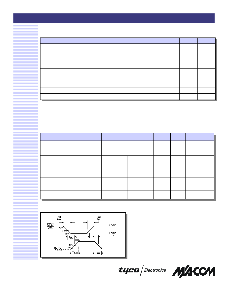
Switching Waveforms

Single/Quad Drivers for GaAs FET Switches and Attenuators
SWD-109/119
Specifications subject to change without notice.
n
North America: Tel. (800) 366-2266
n
Asia/Pacific: Tel.+81-44-844-8296, Fax +81-44-844-8298
n
Europe: Tel. +44 (1344) 869 595, Fax+44 (1344) 300 020
Visit www.macom.com for additional data sheets and product information.
V 4.00
3
Truth Table for Single Driver
(SWD-109)
Input
C1
A
B
Logic "0"
V
EE
V
OPT
Logic "1"
V
OPT
V
EE
Outputs
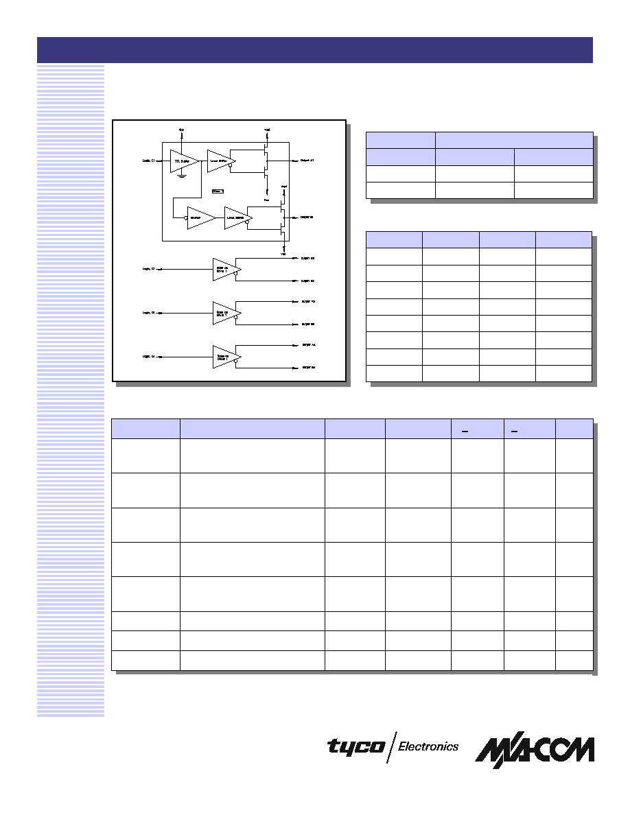
Functional Schematic (SWD-109)
Symbol
Parameter
V
OPT
- V
EE
-55 to +25�C
<+85�C
<+125�C
Unit
T
PLH
Propagation Delay
4.5
6.5
8.5
45
44
43
55
54
52
61
59
57
ns
T
PHL
Propagation Delay
4.5
6.5
8.5
45
43
41
55
52
49
61
57
53
ns
T
TLH
Output Rising Transition Time
4.5
6.5
8.5
10.0
9.0
8.0
10.0
9.0
8.0
11.0
9.0
8.0
ns
T
THL
Output Rising Transition Time
4.5
6.5
8.5
10.0
9.0
8.0
10.0
9.0
8.0
11.0
9.0
8.0
ns
T
skew
Delay Skew, Output A to Output B
4.5
6.5
8.5
8.0
8.0
7.5
8.5
8.5
8.0
10.0
10.0
9.5
ns
C
IN
Input Capacitance
--
10
10
10
pF
C
PDC
Power Dissipation Capacitance
4
--
10
10
10
pF
C
PDE
Power Dissipation Capacitance
4
--
140
140
140
pF
AC Characteristics Over Guaranteed Operating Range
3
(SWD-109)
3. V
CC
= 4.5V, V
EE
= -4.5V, V
OPT
= 0V, C
L
= 25 pF, Trise, Tfall = 6ns. These conditions represent the worst case for slow delays.
4. Total Power Dissipation is calculated by the following formula: PD = V
CC
2
fC
PDC
+ (V
OPT
-V
EE
)
2
fC
PDE
Pin No.
Function
Pin No.
Function
1
Output A
5
Vee
2
GND
6
Vopt
3
Vcc
7
GND
4
C1, Logic
8
Output B
Pin Configuration
Single/Quad Drivers for GaAs FET Switches and Attenuators
SWD-109/119
Specifications subject to change without notice.
n
North America: Tel. (800) 366-2266
n
Asia/Pacific: Tel.+81-44-844-8296, Fax +81-44-844-8298
n
Europe: Tel. +44 (1344) 869 595, Fax+44 (1344) 300 020
Visit www.macom.com for additional data sheets and product information.
V 4.00
4
Functional Schematic (SWD-119)
Truth Table for Quad Driver
(SWD-119)
Input
CX
A
B
Logic "0"
V
EE
V
OPT
Logic "1"
V
OPT
V
EE
Outputs
Pin No.
Function
Pin No.
Function
1
Vee
9
Output A1
2
Vcc
10
Output B1
3
C4
11
Output A2
4
C3
12
Output B2
5
C2
13
Output A3
6
C1
14
Output B3
7
Vopt
15
Output A4
8
GND
16
Output B4
Pin Configuration
Symbol
Parameter
V
OPT
- V
EE
-55 to +25�C
<+85�C
<+125�C
Unit
T
PLH
Propagation Delay
4.5
6.5
8.5
45
44
43
55
54
52
61
59
57
ns
T
PHL
Propagation Delay
4.5
6.5
8.5
45
43
41
55
52
49
61
57
53
ns
T
TLH
Output Rising Transition Time
4.5
6.5
8.5
10.5
10.0
9.0
11.0
10.0
9.0
12.0
10.0
9.0
ns
T
THL
Output Rising Transition Time
4.5
6.5
8.5
10.0
9.0
8.0
10.0
9.0
8.0
11.0
9.0
8.0
ns
T
skew
Delay Skew, Output A to Output B
4.5
6.5
8.5
8.0
8.0
7.5
8.5
8.5
8.0
10.0
10.0
9.5
ns
C
IN
Input Capacitance
--
10
10
10
pF
C
PDC
Power Dissipation Capacitance
4
--
10
10
10
pF
C
PDE
Power Dissipation Capacitance
4
--
140
140
140
pF
AC Characteristics Over Guaranteed Operating Range
3
(SWD-119)
3. V
CC
= 4.5V, V
EE
= -4.5V, V
OPT
= 0V, C
L
= 25 pF, Trise, Tfall = 6ns. These conditions represent the worst case for slow delays.
4. Total Power Dissipation is calculated by the following formula: PD = V
CC
2
fC
PDC
+ (V
OPT
-V
EE
)
2
fC
PDE
Single/Quad Drivers for GaAs FET Switches and Attenuators
SWD-109/119
Specifications subject to change without notice.
n
North America: Tel. (800) 366-2266
n
Asia/Pacific: Tel.+81-44-844-8296, Fax +81-44-844-8298
n
Europe: Tel. +44 (1344) 869 595, Fax+44 (1344) 300 020
Visit www.macom.com for additional data sheets and product information.
V 4.00
5
Ordering Information
Part Number
Package
SWD-109 PIN
SOIC 8 Lead
SWD-109TR
Forward Tape and Reel
SWD-109RTR
Reverse Tape and Reel
Part Number
Package
SWD-119 PIN
SOIC 16 Lead
SWD-119TR
Forward Tape and Reel
SWD-119RTR
Reverse Tape and Reel