 | –≠–ª–µ–∫—Ç—Ä–æ–Ω–Ω—ã–π –∫–æ–º–ø–æ–Ω–µ–Ω—Ç: TB62710P | –°–∫–∞—á–∞—Ç—å:  PDF PDF  ZIP ZIP |

TB62710P/F/FN
TOAHIBA Bi-CMOS Integrated Circuit Silicon Monolithic
TB62710P, TB62710F, TB62710FN
8-Bit Constant-Current LED Driver for Cathode Common LED
The TB62710P, TB62710F and TB62710FN are specifically
designed for use as LED and LED display (cathode-common)
Constant-current drivers.
The constant-current output circuits can be set up using an
external resistor (IOUT = -90 mA max).
These ICs are monolithic integrated circuits have been
designed using the Bi-CMOS process.
The devices consist of an 8-bit shift register, a latch, an
ANDgate and constant-current drivers.
FEATURES
∑ Constant-current output:
A single resistor can be used to set any output current in the
range -5~-90 mA.
∑ Maximum clock frequency: f
CLK
= 15 MHz
(operating while connected in cascade, T
opr
= 25∞C)
∑ 5-V CMOS compatible input
∑ Packages:
P-type:
DIP20-P-300-2.54A
F-type:
SSOP24-P-300-1.00
FN-type:
SSOP20-P-225-0.65A
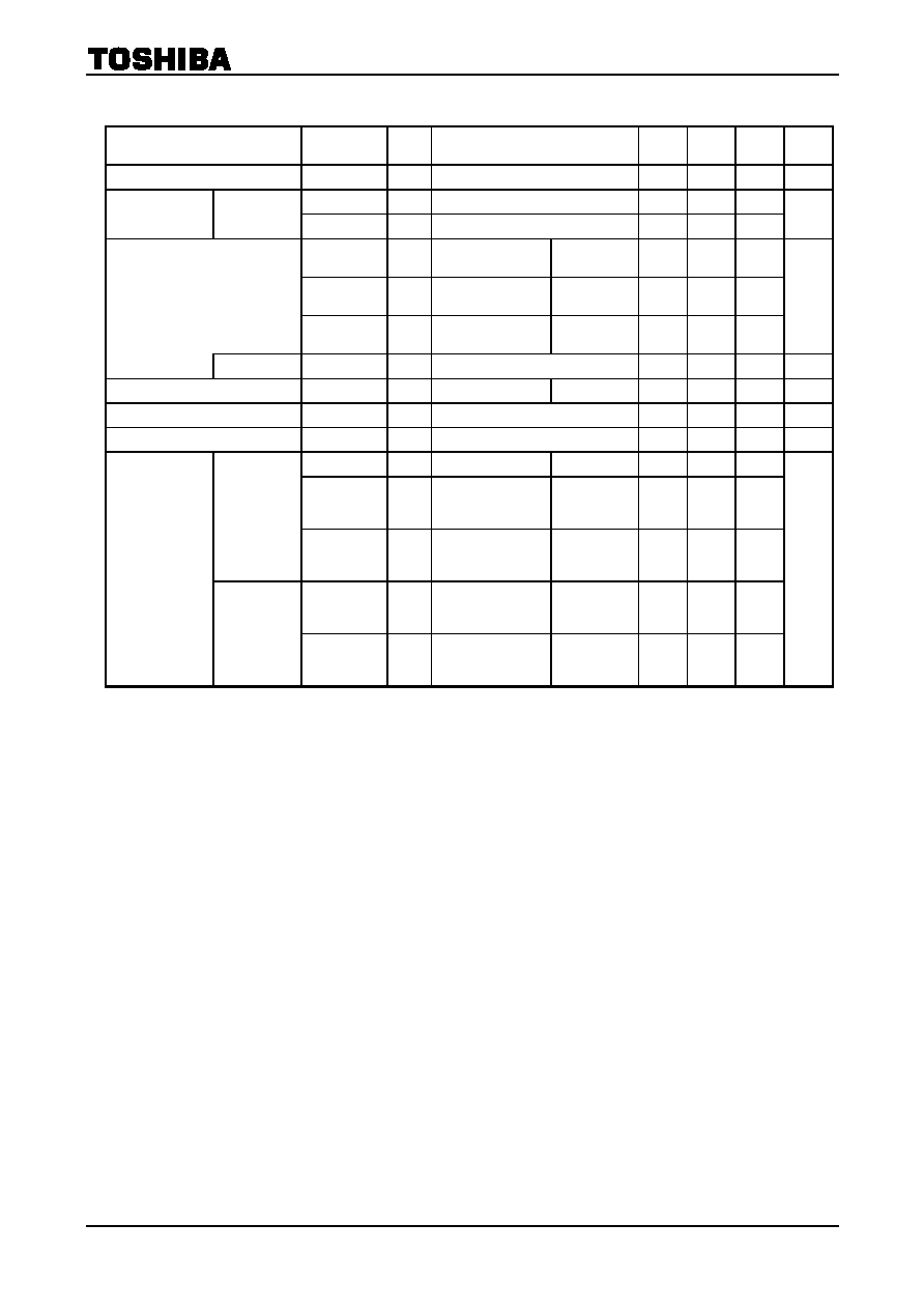
∑ Constant-output-current accuracy:
Current accuracy
Output
- GND
Voltage
between bits
between ICs
Output Current
(max)
>
= 2.0 V (min)
-5~-90 mA
>
= 1.5 V (min)
±6%
±15%
-5~-40 mA
TB62710P
TB62710F
TB62710FN
Weight:
DIP20-P-300-2.54A: 2.25 g (Typ.)
SSOP24-P-300-1.00: 0.33 g (Typ.)
SSOP20-P-225-0.65A: 0.10 g (Typ.)
Web: www.marktechopto.com | Email: info@marktechopto.com
Company Headquarters
3 Northway Lane North
Latham, New York 12110
Toll Free: 800.984.5337
Fax:
518.785.4725
California Sales Office:
950 South Coast Drive, Suite 265
Costa Mesa, California 92626
Toll Free: 800.984.5337
Fax: 714.850.9314

TB62710P/F/FN
2001-04-16
2
Pin Assignment
(top view)
Block Diagram
Truth Table
CLOCK
LATCH
ENABLE SERIAL-IN
OUT0... OUT5 ... OUT7
SERIAL-OUT
H L
Dn Dn
... Dn
- 5 ... Dn - 7
Dn
- 7
L L
Dn
+ 1
No Change
Dn
- 6
H L
Dn
+ 2
Dn
+ 2 ... Dn - 3 ... Dn - 5
Dn
- 5
X L
Dn
+ 3
Dn
+ 2 ... Dn - 3 ... Dn - 5
Dn
- 5
X H
Dn
+
3 OFF Dn
- 5
Note 1: OUT0~OUT7
= ON when Dn = "H"; OUT0~OUT7 = OFF when Dn = "L".
In order to ensure that the level of the power supply voltate is correct, an external resistor must be
connected between R-EXT and GND.
GND
SERIAL-IN
LATCH
CLOCK
NC
V
CC
OUT0
OUT1
V
DD
R-EXT
SERIAL-OUT1
ENABLE
SERIAL-OUT2
V
CC
OUT7
OUT6
P- & FN-types
OUT2
OUT5
OUT3
OUT4
GND
SERIAL-IN
LATCH
CLOCK
NC
V
CC
OUT0
OUT1
V
DD
R-EXT
SERIAL-OUT1
ENABLE
SERIAL-OUT2
NC
OUT7
OUT6
F-type
OUT2
OUT5
OUT3
OUT4
NC
NC
NC
V
CC
SERIAL-IN
LATCH
R-EXT
ENABLE
I-REG
Q
ST D
Q
ST D
D Q
CK
Q
ST D
D Q
CK
D Q
CK
CLOCK
OUT0
OUT1 OUT7
SERIAL-OUT1
V
CC
V
CC
V
CC
D Q
CK
SERIAL-OUT2

TB62710P/F/FN
2001-04-16
3
Timing Diagram
Note 2: The latches circuit holds data by pulling the
LATCH
terminal Low.
And, when
LATCH
terminal is a "H" level, latch circuit doesn't hold data, and it passes from the input to the
output.
When
ENABLE
terminal is a "L" level, output terminal OUT0~ OUT7 respond to the data, and on & off does.
And, when
ENABLE
terminal is a "H" level, it offs with the output terminal regardless of the data.
SERIAL-IN
LATCH
CLOCK
OUT0
OUT1
OUT6
ENABLE
n
=
1
2 3 4 5 6 7 8
SERIAL-OUT2
SERIAL-OUT1
OUT7
OFF
OFF ON
OFF
OFF
OFF ON
OFF
5 V
0 V
5 V
0 V
5 V
0 V
5 V
0 V
5 V
0 V
5 V
0 V

TB62710P/F/FN
2001-04-16
4
Terminal Description
Pin No.
P/FN-Type F-Type
Pin Name
Function
1
1
GND
GND terminal for control logic
2
2
SERIAL-IN
Input terminal for serial data for data shift register
3
3
CLOCK
Input terminal for clock for data shift on rising edge
4 5
LATCH
Input terminal for data strobe
When the
LATCH
input is driven High, data is latched. When it is pulled Low, data
is hold.
6, 15
7, 18
V
CC
0 V~17 V supply voltage terminal for LED
7~14 9~16
OUT0~OUT7
Output
terminals
17 21
ENABLE
Input terminal for output enable.
All outputs (OUT0~OUT7) are turned off, when the ENABLE terminal is driven
High.
And are turned on, when the terminal is driven Low.
16
20
SERIAL-OUT2 Output terminal for serial data input on SERIAL-IN terminal
18
22
SERIAL-OUT1 Output terminal for serial data input on SERIAL-IN terminal
19
23
R-EXT
Input terminal used to connect an external resistor. This regulated the output current.
20 24 V
DD
5-V supply voltage terminal
5
4, 6, 8,
17, 19
NC Not
connected
Equivalent Circuits For Inputs and Outputs
ENABLE terminal
LATCH terminal
CLOCK, SERIAL-IN terminal
SERIAL-OUT1 and SERIAL-OUT2 terminals
CLOCK,
SERIAL-IN
V
DD
GND
300 k
V
DD
ENABLE
GND
R (UP)
V
DD
LATCH
GND
R (DOWN)
200 k
V
DD
GND
SERIAL-OUT1, 2

TB62710P/F/FN
2001-04-16
5
Maximum Ratings
(T
opr
=
=
=
= 25∞C)
Characteristic Symbol Rating Unit
Supply voltage
V
DD
0~7.0 V
Supply voltage for LED
V
LED
0~17.0 V
Input voltage
V
IN
-0.4~V
DD
+ 0.4
V
Output current
I
OUT
-90 mA
Output voltage
V
OUT
-0.4~17 V
Clock frequency
f
CLK
15
MHz
V
CC
terminal current
IV
CC
1440
mA
P-type
(when not mounted)
P
d1
1.47
F-type
(when not mounted)
0.59
F-type (on PCB)
P
d2
0.83
FN-type
(when not mounted)
0.71
Power
Dissipation
(Note 3)
FN-type (on PCB)
P
d3
0.96
W
P-type
(when not mounted)
R
th (j-a) 1
85
F-type
(when not mounted)
210
F-type (on PCB)
R
th (j-a) 2
150
FN-type
(when not mounted)
175
Thermal
Resistance
(Note 3)
FN-type (on PCB)
R
th (j-a) 3
130
∞C/W
Operating Temperature
T
opr
-40~85 ∞C
Storage Temperature
T
stg
-55~150 ∞C
Note 3: P-Type: Powes dissipation is derated by 12.5 mW/∞C if device is mounted on PCB and ambient temperature
is above 25∞C.
F-Type: Powes dissipation is derated by 6.7 mW/∞C if device is mounted on PCB and ambient temperature is
above 25∞C.
With device mounted on PCB of 60% Cu and of dimensions 50 mm
◊ 50 mm ◊ 1.6 mm
FN-Type: Powes dissipation is derated by 7.7 mW/∞C if device is mounted on PCB and ambient temperature
is above 25∞C.
With device mounted on PCB of 40% Cu and of dimensions 50 mm
◊ 50 mm ◊ 1.6 mm

TB62710P/F/FN
2001-04-16
6
Recommended Operating Conditions
(T
opr
=
=
=
=
-
-
-
-
40∞C ~85∞C unless otherwise specified)
Characteristic
Symbol Conditions
Min
Typ.
Max
Unit
Supply voltage
V
DD
4.5 5.0 5.5 V
V
CC1
V
CC
- V
OUT
>
= 2.0 V,
I
OUT
<
= -90 mA
4
17
Supply voltage for LED
V
CC2
V
CC
- V
OUT
>
= 1.5 V,
I
OUT
<
= -40 mA
3.5
17
V
Output voltage
V
OUT
V
CC
common
0
-17 V
I
OUT
DC1
circuit
-5
-78
I
OH
SERIAL-OUT1,
2
-1.0
Output current
I
OL
SERIAL-OUT1,
2
1.0
mA
V
IH
0.7
V
DD
V
DD
+
0.3
Input voltage
V
IL
V
DD
= 4.5~5.5 V
-0.3
0.3
V
DD
V
LATCH
pulse width
t
wLAT
V
DD
= 4.5~5.5 V
100
ns
CLOCK pulse width
t
wCLK
V
DD
= 4.5~5.5 V
50
ns
ENABLE pulse width
t
wENA
V
DD
= 4.5~5.5 V
1000
ns
Set-up time for DATA
t
setup
V
DD
= 4.5~5.5 V
100
ns
Hold time for DATA
t
hold
V
DD
= 4.5~5.5 V
100
ns
Clock frequency
t
CLK
V
DD
= 4.5~5.5 V, Cascade operation
10.0 ns
P-type P
d1
When
not
mounted
0.76
F-type P
d2
0.43
Power Dissipation
FN-type P
d3
T
opr
= 85∞C
On PCB
0.50
W
TB62710P/F/FN
2001-04-16
7
Electrical Characteristics
(T
opr
=
=
=
= 25∞C, V
DD
=
=
=
= 5 V, V
CC
=
=
=
= 17 V unless otherwise specified)
Characteristic
Symbol
Test
circuit
Conditions Min
Typ.
Max
Unit
Output leakage current
I
LEAK
V
CC
= 17.0 V
-10
µA
V
OH
I
OH
= -1.0 mA
0.4
Output voltage
SERIAL-OUT
1, 2
V
OL
I
OL
= 1.0 mA
4.6
V
I
OUT1
V
CC
= 4 V,
V
OUT
= V
CC
- 2.0 V
R
EXT
= 360 -62.1 -73.0 -83.9
I
OUT2
V
CC
= 4 V,
V
OUT
= V
CC
- 2.0 V
R
EXT
= 620 -34.0 -40.0 -46.0
Output current
(including current skewing)
I
OUT3
V
CC
= 3.5 V,
V
OUT
= V
CC
- 1.5 V
R
EXT
= 620 -32.3 -38.0 -43.7
mA
Current
skew
I
OUT
Same as I
OUT1
, I
OUT2
and I
OUT3
±1.5
±6.0 %
Supply voltage regulation
%/V
DD
Ta
= -40~85∞C R
EXT
= 360
1.5 5.0 %/V
Pull-up resistor
R
in (Up)
150 300 600 k
Pull-down resistor
R
in (Down)
100 200 400 k
I
DD (OFF)
All outputs
= OFF
R
EXT
= OPEN
0.6 1.2
I
DD (ON) 1
DATA
= ALL "H",
All outputs
= ON
(no load)
R
EXT
= 360
7.5 10.0
V
DD
I
DD (ON) 2
DATA
= ALL "H",
All outputs
= ON
(no load)
R
EXT
= 620
4.0 7.0
I
CC (OFF)
DATA
= ALL "L",
All outputs
= OFF
(no load)
R
EXT
= 620
0.5 1.0
Supply current
V
CC
I
CC (ON)
DATA
= ALL "H",
All outputs
= ON
(no load)
R
EXT
= 360
42.0 52.0
mA

TB62710P/F/FN
2001-04-16
8
Switching Characteristics
(T
opr
=
=
=
=
25∞C unless otherwise specifed
)
Characteristic
Symbol
Test
circuit
Conditions Min
Typ.
Max
Unit
CLK-OUTn
LATCH
-OUTn
ENABLE -OUTn
200 450
Propagation
delay time
("L" to "H")
CLK-SOUTn
t
pLH
20 70
ns
CLK-OUTn
LATCH
-OUTn
ENABLE -OUTn
60 180
Propagation
delay time
("H" to "L")
CLK-SOUTn
t
pHL
20 70
ns
CLK t
wCLK
20 30
Pulse width
LATCH
t
wLAT
10 25
ns
Set-up time
LATCH
/SIN/
CLOCK
DATA
= "L" "H"
t
setup
25 50 ns
Hold time
LATCH
/SIN/
CLOCK
DATA
= "H" "L"
t
hold
0 30 ns
Rise time
(Note
4)
t
r
10 µs
Slow clock
Fall time
(Note
4)
t
f
10 µs
Output rise time
t
or
25 55 110 ns
Output fall time
t
of
V
DD
= 5.0 V, V
CC
= 17.0 V
V
OUT
= V
CC
- 2.0 V
V
IH
= V
DD
, V
IL
= GND
R
EXT
= 620
C
L
= 10.5 pF
t
or
: 10~90%
t
of
: 90~10%
t
pLH
: 50~10%
t
pHL
: 50~90%
Set the switching
characteristics according to the
result of measuring the voltage
waveform.
250 450 600 ns
Note 4: If the device is connected in a cascade and t
r
/t
f
for the waveform is large, it may not be possible to achieve
the timing required for data transfer. Please consider the timings carefully.

TB62710P/F/FN
2001-04-16
9
Test Circuit
DC Characteristic
AC Characteristic
GND
SERIAL-IN
LATCH
CLOCK
OUT0
SERIAL-OUT1,
SERIAL-OUT2
ENABLE
OUT7
I
IL
, I
IH
V
DD
I
DD
V
IL
, V
IH
I
OUT
V
CC
I
LED
C
L
R
L
C
L
GND
SERIAL-IN
LATCH
CLOCK
OUT0
SERIAL-OUT1, 2
ENABLE
OUT7
V
DD
V
CC
Func
t
i
on
Generat
or
V
IH
, V
IL
R
L
C
L
Logic input
waveform
V
DD
= V
IH
= 5.0 V
V
IL
= 0 V
t
r
= t
f
= 10 ns
(10% to 90%)

TB62710P/F/FN
2001-04-16
10
Timing Waveforms
1. CLOCK, SERIAL OUTn
2. CLOCK, LATCH
3. ENABLE ≠ OUTn
t
r
90%
SERIAL-IN
CLOCK
OUTn
t
r
50%
10%
10%
t
wCLK
50%
50%
50%
t
setup
SERIAL-OUT1
90%
t
of
50%
10%
t
or
10%
50%
90%
t
pLH
t
pHL
50%
t
pLH
50%
t
pHL
SERIAL-OUT2
50%
50%
t
pLH
t
pHL
LATCH
t
wCLK
SERIAL-IN
CLOCK
50%
t
setup
50%
50%
50%
t
wLAT
OUTn
ENABLE
t
pLH
50%
50%
50%
50%
t
pHL
ON
OFF

TB62710P/F/FN
2001-04-16
11
Reference Data
(duty curves
+
+
+
+ package power dissipation)
Duty (%)
I
OUT
(m
A
)
Duty (%)
I
OUT
≠ Duty on PCB
Duty (%)
I
OUT
(m
A
)
I
OUT
≠ Duty on PCB
T
opr
(∞C)
P
d
≠ T
opr
P
d
(
W
/
I
C
)
0
0 25 50
0.5
1.0
1.5
2.0
75 100
P-type FREE AIR
F-type ON PCB
FN-type ON PCB
90
80
60
40
20
0
70
50
30
10
100 1000 10000
25∞C
VDD = 5.0 V,
VCE = 2.0 V,
VCC = 17.0 V
5000
500
IOUT (mA) =
(1.26
˜ REXT ()) ◊ 18
85∞C
Topr = -40∞C
R
EXT
(
)
I
OUT
(m
A
)
I
OUT
≠ R
EXT
I
OUT
≠ Duty on PCB
I
OUT
(m
A
)
0
0 20 40 60 80 100
10
20
30
40
50
60
70
80
Topr = 85∞C,
VCC - VOUT = 2.0 V
Tj
= 120∞C
TB62710FN
TB62710F
TB62710P
0
0 20 40 60 80 100
10
20
30
40
50
60
70
80
Topr = 60∞C,
VCC - VOUT = 2.0 V
Tj
= 120∞C
TB62710FN
TB62710F
TB62710P
0
0 20 40 60 80 100
10
20
30
40
50
60
70
80
Topr = 25∞C,
VCC - VOUT = 2.0 V
Tj
= 120∞C
TB62710FN
TB62710F
TB62710P

TB62710P/F/FN
2001-04-16
12
The bottom figure shows an application circuit.
For best results, this IC should be operated with V
O
= 2.0 V.
V
O
(V) = V
CC
- V
OUT
= V
CC
- V
f
(LED) - V
CE1
When V
CC
is high and the V
f
of the LED is low.
V
O
is also high , the increase in power dissipation may in turn adversely affect the IC's output current.
In this case, reduce the voltage by connecting an external resistor.
In this way the IC's output current can be stabilized.
(max)
number
BIT
(max)
OUT
I
(min)
O
V
f
V
CC
V
R
◊
-
-
=
It is looked for.
it is also possible that the IC will operate in an unstable manner due to the inductance of the wiring.
To counter this, it is recommended that the IC be situated as close as possible on the PCB to the LED module, and
as far as possible from other ICs. Otherwise, there is the risk that the IC will malfunction.
Application
CPU
SCAN
V
DD
n
R
GND
SERIAL-IN
LATCH
CLOCK
OUT0
SERIAL-OUT1,
SERIAL-OUT2
ENABLE
OUT7
V
CC
V
CC
R-EXT
GND
SERIAL-IN
LATCH
CLOCK
OUT0
SERIAL-OUT1,
SERIAL-OUT2
ENABLE
OUT7
V
CC
V
CC
R-EXT
V
LED
= 5~17 (V)
V
O
= V
CC
- V
f (LED)
- V
CE1
For best results, operate at V
O
= 2.0 V
V
CE1

TB62710P/F/FN
2001-04-16
13
Notes
∑ Operation may become unstable due to the electromagnetic interference caused by the wiring and other
phenomena.
To counter this, it is recommended that the IC be situated as close as possible to the LED module.
If overvoltage is caused by inductance between the LED and the output terminals, both the LED and the
terminals may suffer damage as a result.
∑ There is only one GND terminal on this device when the inductance in the GND line and the resistor are large,
the device may malfunction due to the GND noise when output switchings by the circuit board pattern and
wiring.
To achieve stable operation, it is necessary to connect a resistor between the REXT terminal and the GND line.
Fluctuation in the output waveform is likely to occur when the GND line is unstable or when a capacitor (of
more than 50 pF) is used.
Therefore, take care when designing the circuit board pattern layout and the wiring from the controller.
∑ This application circuit is a reference example and is not guaranteed to work in all conditions.
Be sure to check the operation of your circuits.
∑ This device does not include protection circuits for overvoltage, overcurrent or overtemperature.
If protection is necessary, it must be incorporated into the control circuitry.
∑ The device is likely to be destroyed if a short-circuit occurs between either of the power supply pins and any of
the output terminals when designing circuits, pay special attention to the positions of the output terminals and
the power supply terminals (V
DD
and V
LED
), and to the design of the GND line.

TB62710P/F/FN
2001-04-16
14
Package Dimensions
: 2.25 g ()

TB62710P/F/FN
2001-04-16
15
Package Dimensions
: 0.33 g ()

TB62710P/F/FN
2001-04-16
16
Package Dimensions
: .0.10 g ()

TB62710P/F/FN
2001-04-16
17
∑ TOSHIBA is continually working to improve the quality and reliability of its products. Nevertheless, semiconductor
devices in general can malfunction or fail due to their inherent electrical sensitivity and vulnerability to physical
stress. It is the responsibility of the buyer, when utilizing TOSHIBA products, to comply with the standards of
safety in making a safe design for the entire system, and to avoid situations in which a malfunction or failure of
such TOSHIBA products could cause loss of human life, bodily injury or damage to property.
In developing your designs, please ensure that TOSHIBA products are used within specified operating ranges as
set forth in the most recent TOSHIBA products specifications. Also, please keep in mind the precautions and
conditions set forth in the "Handling Guide for Semiconductor Devices," or "TOSHIBA Semiconductor Reliability
Handbook" etc..
∑ The TOSHIBA products listed in this document are intended for usage in general electronics applications
(computer, personal equipment, office equipment, measuring equipment, industrial robotics, domestic appliances,
etc.). These TOSHIBA products are neither intended nor warranted for usage in equipment that requires
extraordinarily high quality and/or reliability or a malfunction or failure of which may cause loss of human life or
bodily injury ("Unintended Usage"). Unintended Usage include atomic energy control instruments, airplane or
spaceship instruments, transportation instruments, traffic signal instruments, combustion control instruments,
medical instruments, all types of safety devices, etc.. Unintended Usage of TOSHIBA products listed in this
document shall be made at the customer's own risk.
∑ The products described in this document are subject to the foreign exchange and foreign trade laws.
∑ The information contained herein is presented only as a guide for the applications of our products. No
responsibility is assumed by TOSHIBA CORPORATION for any infringements of intellectual property or other
rights of the third parties which may result from its use. No license is granted by implication or otherwise under
any intellectual property or other rights of TOSHIBA CORPORATION or others.
∑ The information contained herein is subject to change without notice.
000707EBA
RESTRICTIONS ON PRODUCT USE