TB62736FUG
TOSHIBA BiCD Digital Integrated Circuit Silicon Monolithic
TB62736FUG
Step-up Type DC-DC Converter for White LEDs
The TB62736FUG is a high efficiency step-up type DC/DC
converter that is designed especially for use as a constant current
driver of white LEDs.
It is possible to drive 2 - 6 white LEDs connected in series using a
lithium-ion battery. (Typ. 4 White LEDs)
This IC incorporates an N-ch-MOS transistor required for
switching of an external inductor.
The forward current of the LEDs can be controlled by an external
resistor. An analog voltage input and a pulse input system (PWM)
can be used as a brightness control function.
The switching frequency is fixed at around 1.1 MHz.
This IC is best suited for use as a driver of white LED back
lighting in color LCDs in PDAs, cellular phones and handy
terminal devices.
Features
∑ Brightness control function
: LED forward current 25~100%
∑ Maximum output voltage
: over 24V
∑ LED current values controlled by external resistance
: 20mA (typ.) @ RSENS=16
∑ Output power
: 400 mW
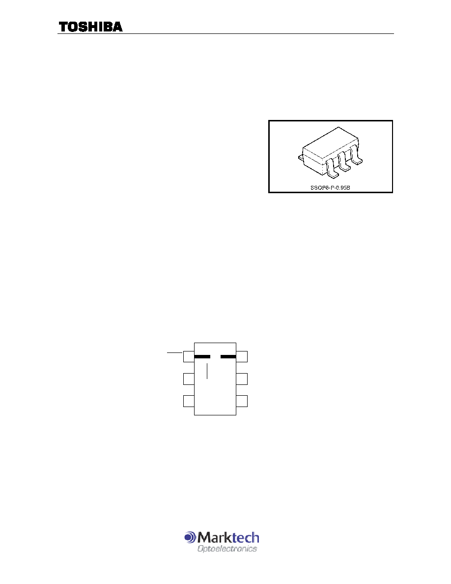
∑ Package
: SSOP6-P-0.95 (SOT23-6)
∑ High efficiency
: maximum 87% (when used with components as recommended herein)
∑ Thermal Shutdown Function incorporated : 150 degree (typ.)
Pin Assignment (top view)
Note 1:
The IC may break if mounted 180 degrees in reverse. Ensure the device is correctly orientated before
assembley
.
Note 2: The control pin must be set to a certain logic level, as unstable output could result if the pin is left open..
Note 3: Regarding soldering, the following conditions were confirmed
(1) Use of Sn-63Pd solder bath
solder
bath
temperature
= 230∞C, dipping time = 5 seconds, number of times = once, use of R-type flux
(2) Use of Sn-3.0Ag-0.5Cu solder bath
solder
bath
temperature
= 245∞C, dipping time = 5 seconds, number of times = once, use of R-type flux
Weight: 0.016 g (typ.)
SHDN
(NC)
VIN
FB
GND
SW
M
Company Headquarters
3 Northway Lane North
Latham, New York 12110
Toll Free: 800.984.5337
Fax:
518.785.4725
Web: www.marktechopto.com | Email: info@marktechopto.com
California Sales Office:
950 South Coast Drive, Suite 265
Costa Mesa, California 92626
Toll Free: 800.984.5337
Fax: 714.850.9314
Company Headquarters
3 Northway Lane North
Latham, New York 12110
Toll Free: 800.984.5337
Fax:
518.785.4725
Web: www.marktechopto.com | Email: info@marktechopto.com
California Sales Office:
950 South Coast Drive, Suite 265
Costa Mesa, California 92626
Toll Free: 800.984.5337
Fax: 714.850.9314

TB62736FUG
2004-10-29
2
Block Diagram
Pin Functions
No. Symbol
Function
1
SHDN
Input pin for IC ON/OFF control and variable LED I
F
.
0 to 0.5V : Shutdown Mode (IC shutdown)
1.0V to 2.5V : I
F
= 25 to 100% Variable (Linear Control)
Over 2.5V : I
F
= 100%
PWM signal input for IF control (see p.5)
2
NC
No Connection or Connected to GND
3
VIN
Supply voltage pin. Supply voltage range : 2.8V to 5.5V
4
SW
DC-DC converter switching pin ≠ switch incorporates N-ch MOSFET
5
GND Ground
pin
6
FB
Connected to the cathode of LED
Note: The NC terminal is not connected to the internal circuit.
Level
Detect
CTL
AMP.
CTL
AMP.
Error
AMP.
Off Time
Control
Mono Multi
Reference
Mono Multi
SW
NC
GND
SHDN
VIN
1
3
4
2
6
5

TB62736FUG
2004-10-29
3
Absolute Maximum Ratings
(T
opr
=
25∞C, unless otherwise specified)
Characteristics Symbol
Ratings
Unit
Power supply voltage
V
IN
-0.3 to 6.0
V
Input voltage
V
in
-0.3 to V
CC
+ 0.3
V
Switching pin voltage
V
O (SW)
-0.3 to 24
V
Switching pin current
I
O (SW)
380 mA
0.41 (IC only)
Power Dissipation
P
D
0.47 (IC mounted on
PCB)
(Note)
W
R
th (j-a) 1
300
(IC
only)
Thermal resistance
R
th (j-a) 2
260 (IC mounted on
PCB)
∞C/W
Operating temperature range
T
opr
-40 to 85
∞C
Storage temperature
T
stg
-40 to 150
∞C
Maximum junction temperature
T
j
125
∞C
Note: Power dissipation is reduced by 3.8mW/∞C from the maximum rating for every 1∞C exceeding the ambient
temperature of 25∞C (when the IC is mounted on a PCB).
Recommended Operating Condition
(T
opr
=
-
40 to 85∞C, unless otherwise specified)
Characteristics Symbol Test
Conditions
Min.
Typ.
Max.
Unit
Power supply voltage
V
IN
2.8
5.5 V
SHDN pin H level input voltage
V
SHDN (H)
2.7
V
IN
V
SHDN pin L level input voltage
V
SHDN (L)
0
0.5 V
SHDN pin input pulse width
tpw
ON/OFF duty width
33
µs
LED current (Average value)
I
O1
V
IN
= 3.6 V, RSENS = 16
4LEDs, T
opr
= 25∞C
20
A
Electrical Characteristics
(T
opr
=
-
40~85∞C V
CC
=
2.8~5.5 V, unless otherwise specified)
Characteristics Symbol Test
Conditions
Min.
Typ.
Max.
Unit
Operating consumption current
I
IN (ON)
V
IN
= 6.0 V, RSENS = 16
0.9 1.5 mA
Standby consumption current
I
IN (OFF)
V
IN
= 3.6 V, V
SHDN
= 0 V
0.5 1.0 µA
SHDN pin current
I
SHDN
V
IN
= 3.6 V, V
SHDN
= 3.6 V
-10 0 10 µA
Integrated MOS-FET switching
frequency
f
OSC
V
IN
= 3.6 V, V
SHDN
= 3.6 V
0.77
1.1
1.43
MHz
Switching pin protection voltage
V
O (SW)
25 V
Switching pin current
I
O (SW)
400 mA
Switching pin leakage current
I
OZ (SW)
0.5 1 µA
FB pin feedback voltage
V
FB
V
IN
= 3.6 V, RSENS = 16
T
opr
= 25∞C, L = 4.7
µH
308 325 342 mV
FB pin line regulation
V
FB
V
IN
= 3.6 V center
V
IN
= 3.0V to 5.0V
-5
5 %

TB62736FUG
2004-10-29
4
Application Circuit Example
Protection at the time of LED opening
The zener diode in the application circuit example is necessary for the provision of over-voltage protection for
when the LED becomes open. As the IC does not incorporate a voltage protection circuit, it is strongly advised that
a zener diode be connected.
The zener diode should satisfy the following conditions:
i)
Less than maximum output voltage of 24V
ii) Greater than the total series LED V
F
iii) Less than the maximum output capacitance C
2
.
Moreover, by connecting a protection circuit such as R_ZD in the figure below, it is possible to control the output
current when the LED becomes open, and to use a zener diode of lower tolerance.
An example of IZD control by R_ZD connection. (RSENS = 16 )
R_DZ (
) IZD
(mA)
500 0.6
100 1.0
In order to avoid adverse effects on driver characteristics,
Toshiba recommends a resistance of 500 ohms or less.
Level
Detect
CTL
AMP.
CTL
AMP.
Error
AMP.
Off Time
Control
Mono Multi
Reference
Mono Multi
1.0-2.5V
Analog
PWM
VIN
SW
NC
FB
GND
SHDN
4.7-10µH
1µF
2.2µF
VIN
16
@20mA
1
3
4
2
6
5
500
Vz=24V
SW
GND FB
S-Di
IZD
1
µF
C2
R_ZD
RSENS
IF
Protection circuit application
TB62736FUG
2004-10-29
5
Output-side Capacitor Setting
It is recommended that the value of C2 be equal to, or greater than 1.0 (µF).
External Inductor Size Setting
For each number of LEDs, the selected inductance should be greater than the value indicated in the
table below.
Number of LEDs
Inductance (Unit:
µH) Note
2 4.7
3
4
6.8
5
6
10
I
F
= 20 mA
Control of I
F
The resistance RSENS is connected between the FB pin and the GND pin.
The average current is controlled by the RSENS value, and calculated using the following equation:
I
F
(mA) = [ 325mV / RSENS() ]
Margin of error is ±5%.
Current control using SHDN pin
This IC can carry out variable of the IF current by external resistance Variable range : 30 to 100%
SHDN Voltage
VSHDN=0V~0.5V
VSHDN=1V~2.5V
VSHDN>2.5V
Note
Io Valuable Rate
0
25 - 100
100
UNIT : %
Dimming using PWM signal input
A dimming function can also by applied using a PWM signal.
[Notes]
When using a PWM signal, the minimum pulse width of the PWM should be greater than 33µs.
Duty ratio of PWM function should be set at 10% - 90%.
The recommended PWM frequency should be 100Hz - 10kHz.
<<Output current is calculated using the following equation>>
IF(mA) =
RSENS []
325[mV] ◊ ON Duty [%]
SHDN input - output rate/output current
VIN=3.0V
0
20
40
60
80
100
1.0
1.3
1.6
1.9
2.2
2.5
VSHDN(V)
IF
r
a
te
(
%
)
0
5
10
15
20
25
IF
(
m
A)
IF rate
IF
TB62736FUG
2004-10-29
6
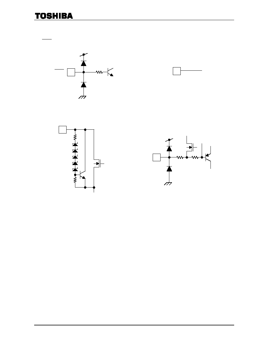
I/O Equivalent Pin Circuits
1. SHDN
pin
2. NC pin
3. SW
pin
4. FB pin
4
1k
20k
SW
VIN
6
20k
5k
FB
The NC pin is not connected to any internal circuit.
VIN
1
50k
SHDN
2
NC

TB62736FUG
2004-10-29
7
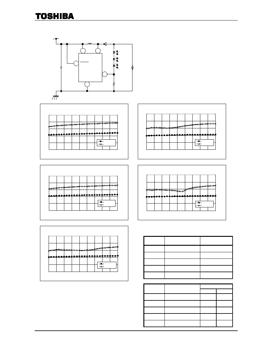
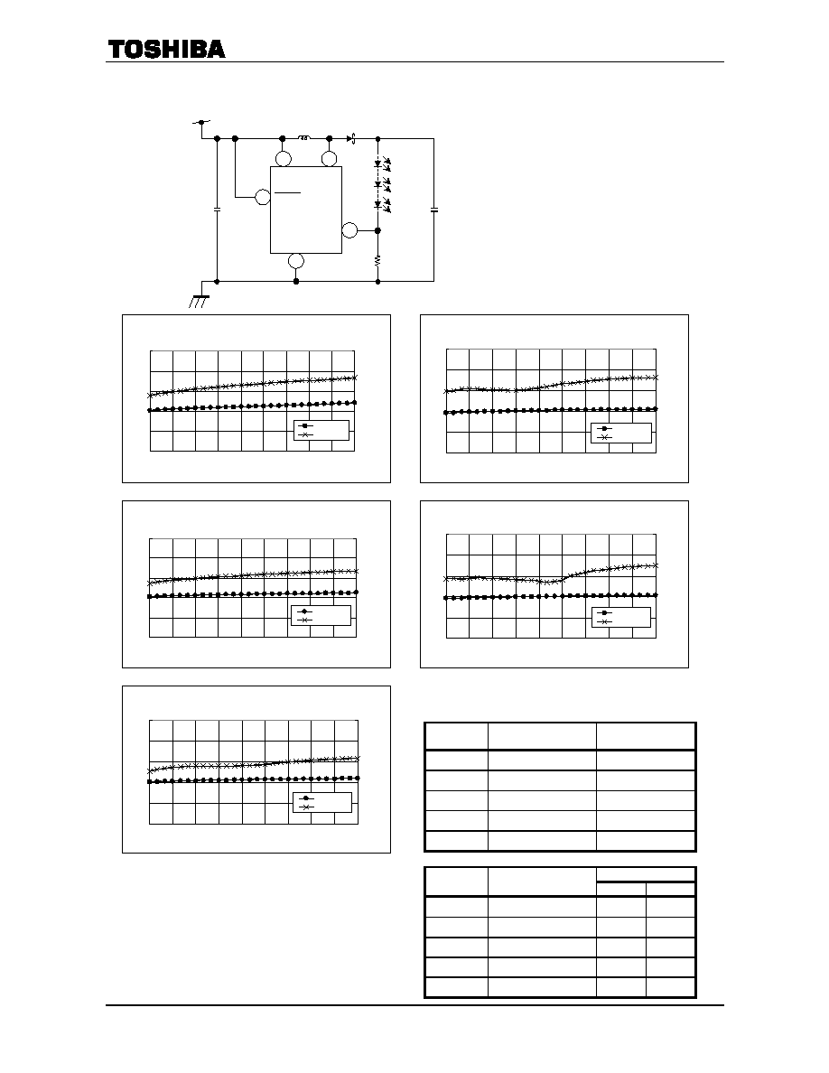
1. Application Circuit Example and Measurement Data (Reference data)
∑ Evaluation conditions
L
: CXLD120 series (NEO MAX CO.,Ltd.)
(Size 2.5
◊ 3.0 ◊ 1.2 mm)
S-Di
: CUS02 1 A/30 V (TOSHIBA Corp.)
LED
: NSCW215T (NICHIA Corp.)
C1
: C2012JB1E105K (TDK Corp.)
C2
: C2012JB1E105K (TDK Corp.)
R
S
EN
S
=
1.
6
V
IN
=
2.8~5.5 V
L
1
S-Di
C
2
=
1.
0
µ
F
V
CC
SW
SHDN
GND
FB
C
1
=
2.
2
µ
F
2~6
WLEDs
Input Voltage - Efficiency/Output Current
2LED Drive, L=4.7µH
10
15
20
25
30
35
2.8
3.1
3.4
3.7
4
4.3
4.6
4.9
5.2
5.5
VIN(V)
IO
U
T
(
m
A
)
50
60
70
80
90
100
E
f
f
i
ci
e
n
cy
(
%
)
IOUT
Efficiency
Input Voltage - Efficiency/Output Current
3LED Drive, L=6.8µH
10
15
20
25
30
35
2.8
3.1
3.4
3.7
4
4.3
4.6
4.9
5.2
5.5
VIN(V)
IO
U
T
(
m
A
)
50
60
70
80
90
100
Ef
f
i
cie
n
cy
(
%
)
IOUT
Efficiency
Input Voltage - Efficiency/Output Current
4LED Drive, L=6.8µH
10
15
20
25
30
35
2.8
3.1
3.4
3.7
4
4.3
4.6
4.9
5.2
5.5
VIN(V)
IO
U
T
(
m
A
)
50
60
70
80
90
100
E
ffi
c
i
e
n
c
y
(
%
)
IOUT
Efficiency
Input Voltage - Efficiency/Output Current
5LED Drive, L=10µH
10
15
20
25
30
35
2.8
3.1
3.4
3.7
4
4.3
4.6
4.9
5.2
5.5
VIN(V)
IO
U
T
(
m
A
)
50
60
70
80
90
100
E
ffi
c
i
e
n
c
y
(
%
)
IOUT
Efficiency
Input Voltage - Efficiency/Output Current
6LED Drive, L=10µH
10
15
20
25
30
35
2.8
3.1
3.4
3.7
4
4.3
4.6
4.9
5.2
5.5
VIN(V)
IO
U
T
(
m
A
)
50
60
70
80
90
100
Ef
f
i
cie
n
cy
(
%
)
IOUT
Efficiency
<Measurement Data>
Efficiency in the range of V
IN
= 2.8 to 5.5 V
Efficiency
(%)
Average Efficiency
(%)
2 LED
82.60 to 88.46
86.29
3 LED
82.69 to 87.78
85.95
4 LED
80.73 to 86.22
83.05
5 LED
80.73 to 87.28
83.45
6 LED
79.78 to 85.55
81.15
Output current in the range of V
IN
= 3.0 to 5.0 V
Tolerance (%)
Output Current (mA)
V
IN
= 3.6 V center
MIN MAX
2 LED
21.13
-3.50
1.77
3 LED
20.60
-1.95
1.38
4 LED
20.87
-1.75
1.11
5 LED
20.06
-1.81
1.15
6 LED
19.90
-1.95
1.28
TB62736FUG
2004-10-29
8
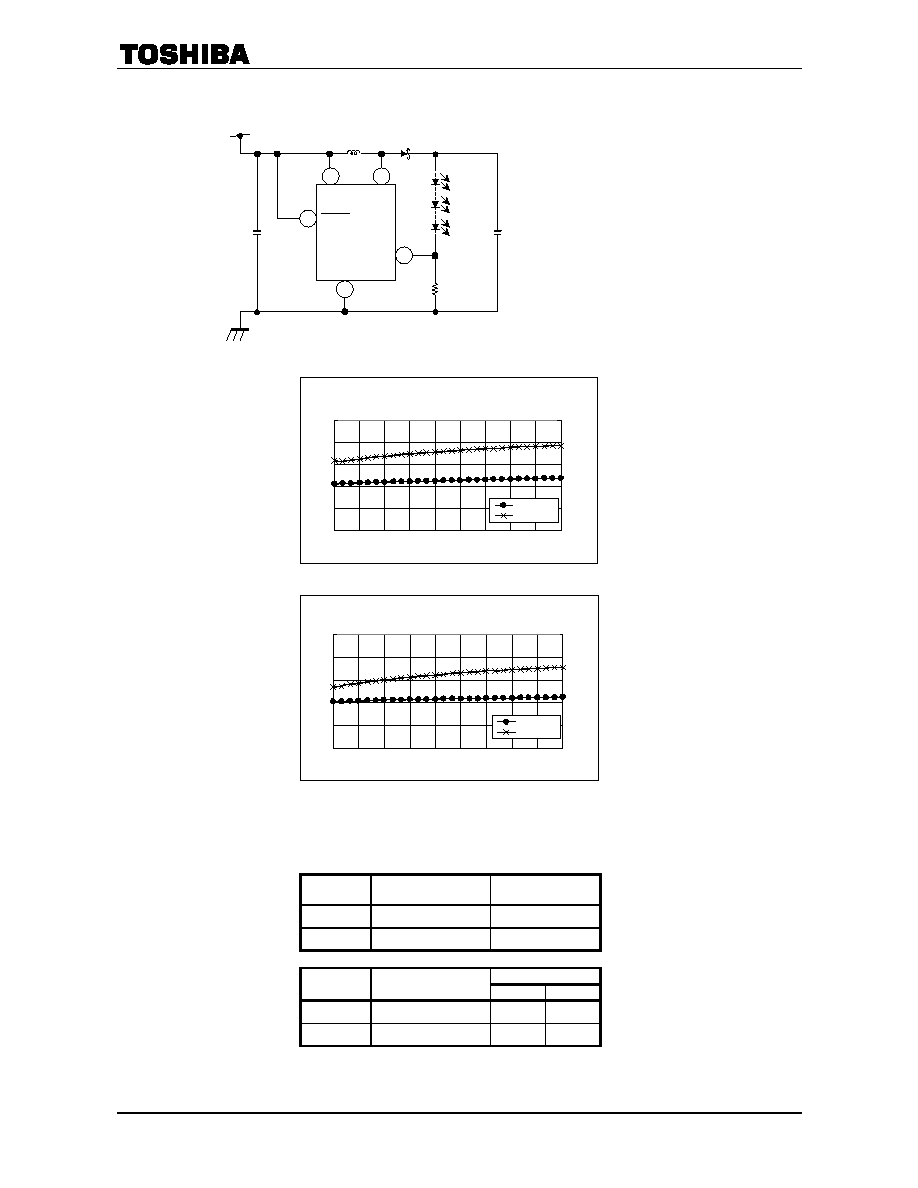
2. Application Circuit Example and Measurement Data (Reference data)
R
SEN
S
=
1.
6
V
IN
=
2.8~5.5 V
L
1
S-Di
C
2
=
1.
0
µ
F
V
CC
SW
SHDN
GND
FB
C
1
=
2.
2
µ
F
2~6
WLEDs
Input Voltage - Efficiency/Output Current
2LED Drive, L=4.7µH
10
15
20
25
30
35
2.8
3.1
3.4
3.7
4
4.3
4.6
4.9
5.2
5.5
VIN(V)
IO
U
T
(
m
A
)
50
60
70
80
90
100
Ef
f
i
c
i
e
n
c
y
(
%
)
Efficiency
IOUT
Input Voltage - Efficiency/Output Current
3LED Drive, L=6.8µH
10
15
20
25
30
35
2.8
3.1
3.4
3.7
4
4.3
4.6
4.9
5.2
5.5
VIN(V)
IO
U
T
(
m
A
)
50
60
70
80
90
100
E
f
f
i
ci
e
n
cy
(%
)
IOUT
Efficiency
Input Voltage - Efficiency/Output Current
4LED Drive, L=6.8µH
10
15
20
25
30
35
2.8
3.1
3.4
3.7
4
4.3
4.6
4.9
5.2
5.5
VIN(V)
IO
U
T
(
m
A
)
50
60
70
80
90
100
E
f
f
i
ci
e
n
cy
(%
)
IOUT
Efficiency
Input Voltage - Efficiency/Output Current
5LED Drive, L=10µH
10
15
20
25
30
35
2.8
3.1
3.4
3.7
4
4.3
4.6
4.9
5.2
5.5
VIN(V)
IO
U
T
(
m
A
)
50
60
70
80
90
100
E
f
f
i
ci
e
n
cy
(%
)
IOUT
Efficiency
Input Voltage - Efficiency/Output Current
6LED Drive, L=10µH
10
15
20
25
30
35
2.8
3.1
3.4
3.7
4
4.3
4.6
4.9
5.2
5.5
VIN(V)
IO
U
T
(
m
A
)
50
60
70
80
90
100
E
f
f
i
ci
e
n
cy
(
%
)
IOUT
Efficiency
∑ Evaluation conditions
L
: 1001AS series (TOKO, INC)
(Size 3.6
◊ 3.6 ◊ 1.2 mm)
S-Di
: CUS02 1 A/30 V (TOSHIBA Corp.)
LED
: NSCW215T (NICHIA Corp.)
C1
: C2012JB1E105K (TDK Corp.)
C2
: C2012JB1E105K (TDK Corp.)
<Measurement Data>
Efficiency in the range of V
IN
= 2.8 to 5.5 V
Efficiency
(%)
Average Efficiency
(%)
2 LED
83.10 to 88.60
86.55
3 LED
81.32 to 86.47
84.54
4 LED
79.15 to 84.63
81.30
5 LED
79.72 to 86.39
82.87
6 LED
78.91 to 85.10
80.47
Output current in the range of V
IN
= 3.0 to 5.0 V
Tolerance (%)
Output Current (mA)
V
IN
= 3.6 V center
MIN MAX
2 LED
21.17
-3.32
1.73
3 LED
20.85
-1.95
1.38
4 LED
20.56
-1.79
1.15
5 LED
20.10
-1.82
1.22
6 LED
19.95
-1.94
1.26

TB62736FUG
2004-10-29
9
3. Application Circuit Example and Measurement Data (Reference data)
R
SEN
S
=
1.
6
V
IN
=
2.8~5.5 V
L
1
S-Di
C
2
=
1.
0
µ
F
V
CC
SW
SHDN
GND
FB
C
1
=
2.
2
µ
F
2~6
WLEDs
∑ Evaluation conditions
L
: LQH2M series (Murata Manufacturing Co.,Ltd.)
(Size 2.0
◊ 1.6 ◊ 0.95 mm)
S-Di
: CUS02 1 A/30 V (TOSHIBA Corp.)
LED
: NSCW215T (NICHIA Corp.)
C1
: C2012JB1E105K (TDK Corp.)
C2
: C2012JB1E105K (TDK Corp.)
Input Voltage - Efficiency/Output Current
2LED Drive, L=4.7µH
10
15
20
25
30
35
2.8
3.1
3.4
3.7
4
4.3
4.6
4.9
5.2
5.5
VIN(V)
IO
U
T
(
m
A
)
50
60
70
80
90
100
E
f
f
i
ci
e
n
cy
(%
)
Efficiency
IOUT
Input Voltage - Efficiency/Output Current
3LED Drive, L=6.8µH
10
15
20
25
30
35
2.8
3.1
3.4
3.7
4
4.3
4.6
4.9
5.2
5.5
VIN(V)
IO
U
T
(
m
A
)
50
60
70
80
90
100
E
f
f
i
ci
e
n
cy
(%
)
IOUT
Efficiency
Input Voltage - Efficiency/Output Current
4LED Drive, L=6.8µH
10
15
20
25
30
35
2.8
3.1
3.4
3.7
4
4.3
4.6
4.9
5.2
5.5
VIN(V)
IO
U
T
(
m
A
)
50
60
70
80
90
100
E
f
f
i
ci
e
n
cy
(%
)
IOUT
Efficiency
Input Voltage - Efficiency/Output Current
5LED Drive, L=10µH
10
15
20
25
30
35
2.8
3.1
3.4
3.7
4
4.3
4.6
4.9
5.2
5.5
VIN(V)
IO
U
T
(
m
A
)
50
60
70
80
90
100
E
f
f
i
ci
e
n
cy
(%
)
IOUT
Efficiency
Input Voltage - Efficiency/Output Current
6LED Drive, L=10µH
10
15
20
25
30
35
2.8
3.1
3.4
3.7
4
4.3
4.6
4.9
5.2
5.5
VIN(V)
IO
U
T
(
m
A
)
50
60
70
80
90
100
E
f
f
i
ci
e
n
cy
(
%
)
IOUT
Efficiency
<Measurement Data>
Efficiency in the range of V
IN
= 2.8 to 5.5 V
Efficiency
(%)
Average Efficiency
(%)
2 LED
82.37 to 88.70
86.38
3 LED
80.19 to 86.55
84.12
4 LED
78.11 to 84.54
80.16
5 LED
74.79 to 84.94
79.94
6 LED
74.14 to 83.47
77.17
Output current in the range of V
IN
= 3.0 to 5.0 V
Tolerance (%)
Output Current (mA)
V
IN
= 3.6 V center
MIN MAX
2 LED
21.19
-3.26
1.69
3 LED
20.90
-1.87
2.17
4 LED
20.63
-1.78
1.01
5 LED
20.09
-1.88
1.25
6 LED
19.93
-1.99
1.07
TB62736FUG
2004-10-29
10
4. Application Circuit Example and Measurement Data (Reference data)
∑ Evaluation conditions
L
: VLF3010A series (TDK Corp.)
(Size 3.0
◊ 3.0 ◊ 1.0 mm)
S-Di
: CUS02 1 A/30 V (TOSHIBA Corp.)
LED
: NSCW215T (NICHIA Corp.)
C1
: C2012JB1E105K (TDK Corp.)
C2
: C2012JB1E105K (TDK Corp.)
RS
E
N
S
=
1.
6
V
IN
=
2.8~5.5 V
L
1
S-Di
C
2
=
1.
0
µ
F
V
CC
SW
SHDN
GND
FB
C
1
=
2.
2
µ
F
2~6
WLEDs
Input Voltage - Efficiency/Output Current
2LED Drive, L=4.7µH
10
15
20
25
30
35
2.8
3.1
3.4
3.7
4
4.3
4.6
4.9
5.2
5.5
VIN(V)
IO
U
T
(
m
A
)
50
60
70
80
90
100
E
f
f
i
ci
e
n
cy
(
%
)
Efficiency
IOUT
Input Voltage - Efficiency/Output Current
3LED Drive, L=6.8µH
10
15
20
25
30
35
2.8
3.1
3.4
3.7
4
4.3
4.6
4.9
5.2
5.5
VIN(V)
IO
U
T
(
m
A
)
50
60
70
80
90
100
E
f
f
i
ci
e
n
cy
(
%
)
IOUT
Efficiency
Input Voltage - Efficiency/Output Current
4LED Drive, L=6.8µH
10
15
20
25
30
35
2.8
3.1
3.4
3.7
4
4.3
4.6
4.9
5.2
5.5
VIN(V)
IO
U
T
(
m
A
)
50
60
70
80
90
100
E
f
f
i
ci
e
n
cy
(
%
)
IOUT
Efficiency
Input Voltage - Efficiency/Output Current
5LED Drive, L=10µH
10
15
20
25
30
35
2.8
3.1
3.4
3.7
4
4.3
4.6
4.9
5.2
5.5
VIN(V)
IO
U
T
(
m
A
)
50
60
70
80
90
100
E
f
f
i
ci
e
n
cy
(
%
)
IOUT
Efficiency
Input Voltage - Efficiency/Output Current
6LED Drive, L=10µH
10
15
20
25
30
35
2.8
3.1
3.4
3.7
4
4.3
4.6
4.9
5.2
5.5
VIN(V)
IO
U
T
(
m
A
)
50
60
70
80
90
100
E
ffi
c
i
e
n
c
y
(
%
)
IOUT
Efficiency
<Measurement Data>
Efficiency in the range of V
IN
= 2.8 to 5.5 V
Efficiency
(%)
Average Efficiency
(%)
2 LED
79.8586.97
84.02
3 LED
80.1985.32
83.39
4 LED
78.7783.60
80.69
5 LED
79.7286.39
82.87
6 LED
78.9185.10
80.49
Output current in the range of V
IN
= 3.0 to 5.0 V
Tolerance (%)
Output Current (mA)
V
IN
= 3.6 V center
MIN MAX
2 LED
21.19
-3.08
1.67
3 LED
20.89
-1.86
1.33
4 LED
20.64
-1.68
1.11
5 LED
20.10
-1.82
1.22
6 LED
19.95
-1.94
1.26
TB62736FUG
2004-10-29
11
5. Application Circuit Example and Measurement Data (Reference data)
∑ Evaluation conditions
L
: 32R51 (KOA Corp.)
(Size 3.2
◊ 2.5 ◊ 0.6 mm)
S-Di
: CUS02 1 A/30 V (TOSHIBA Corp.)
LED
: NSCW215T (NICHIA Corp.)
C1
: C2012JB1E105K (TDK Corp.)
C2
: C2012JB1E105K (TDK Corp.)
R
SEN
S
=
1.
6
V
IN
=
2.8~5.5 V
L
1
S-Di
C
2
=
1.
0
µ
F
V
CC
SW
SHDN
GND
FB
C
1
=
2.
2
µ
F
2~3
WLEDs
Input Voltage - Efficiency/Output Current
2LED Drive, L=5.1µH
10
15
20
25
30
35
2.8
3.1
3.4
3.7
4
4.3
4.6
4.9
5.2
5.5
VIN(V)
IO
U
T
(m
A
)
50
60
70
80
90
100
E
f
f
i
ci
enc
y(
%
)
IOUT
Efficiency
Input Voltage - Efficiency/Output Current
3LED Drive, L=5.1µH
10
15
20
25
30
35
2.8
3.1
3.4
3.7
4
4.3
4.6
4.9
5.2
5.5
VIN(V)
IO
U
T
(m
A
)
50
60
70
80
90
100
E
f
f
i
ci
e
n
c
y(
%)
IOUT
Efficiency
<Measurement Data>
Efficiency in the range of V
IN
= 2.8 to 5.5 V
Efficiency
(%)
Average Efficiency
(%)
2 LED
81.7888.79
85.84
3 LED
76.8485.48
82.17
Output current in the range of V
IN
= 3.0 to 5.0 V
Tolerance (%)
Output Current (mA)
V
IN
= 3.6 V center
MIN MAX
2 LED
21.19
-2.99
1.64
3 LED
20.71
-1.98
1.44
TB62736FUG
2004-10-29
12
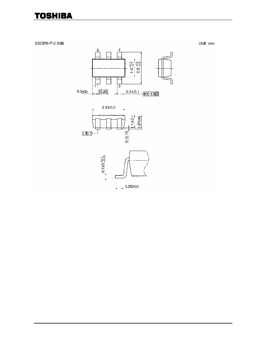
Package Dimensions
Weight: 0.016 g (typ.)

TB62736FUG
2004-10-29
13
∑ The information contained herein is subject to change without notice.
∑ The information contained herein is presented only as a guide for the applications of our products. No
responsibility is assumed by TOSHIBA for any infringements of patents or other rights of the third parties which
may result from its use. No license is granted by implication or otherwise under any patent or patent rights of
TOSHIBA or others.
∑ TOSHIBA is continually working to improve the quality and reliability of its products. Nevertheless, semiconductor
devices in general can malfunction or fail due to their inherent electrical sensitivity and vulnerability to physical
stress. It is the responsibility of the buyer, when utilizing TOSHIBA products, to comply with the standards of
safety in making a safe design for the entire system, and to avoid situations in which a malfunction or failure of
such TOSHIBA products could cause loss of human life, bodily injury or damage to property.
In developing your designs, please ensure that TOSHIBA products are used within specified operating ranges as
set forth in the most recent TOSHIBA products specifications. Also, please keep in mind the precautions and
conditions set forth in the "Handling Guide for Semiconductor Devices," or "TOSHIBA Semiconductor Reliability
Handbook" etc..
∑ The TOSHIBA products listed in this document are intended for usage in general electronics applications
(computer, personal equipment, office equipment, measuring equipment, industrial robotics, domestic appliances,
etc.). These TOSHIBA products are neither intended nor warranted for usage in equipment that requires
extraordinarily high quality and/or reliability or a malfunction or failure of which may cause loss of human life or
bodily injury ("Unintended Usage"). Unintended Usage include atomic energy control instruments, airplane or
spaceship instruments, transportation instruments, traffic signal instruments, combustion control instruments,
medical instruments, all types of safety devices, etc.. Unintended Usage of TOSHIBA products listed in this
document shall be made at the customer's own risk.
∑ The products described in this document are subject to the foreign exchange and foreign trade laws.
∑ TOSHIBA products should not be embedded to the downstream products which are prohibited to be produced
and sold, under any law and regulations.
030619EBA
RESTRICTIONS ON PRODUCT USE