 | –≠–ª–µ–∫—Ç—Ä–æ–Ω–Ω—ã–π –∫–æ–º–ø–æ–Ω–µ–Ω—Ç: GT-48006A | –°–∫–∞—á–∞—Ç—å:  PDF PDF  ZIP ZIP |

GT-48006A
Low Cost Two Port 10/100 Ethernet
Bridge/Switch Controller
Preliminary
Revision 1.2
8/4/98
Please contact Galileo Technology for possible
updates before finalizing a design.
FEATURES
www.galileoT.com support@galileoT.com Tel: +1-408.367.1400 Fax: +1-408.367.1401
∑ Single-chip, low-cost, two port 10/100Mbps Ethernet
bridge/switch
- Provides packet switching functions between two
10/100Mbps, auto-negotiated on-chip Fast
Ethernet ports
- Ideal for dual speed repeater and 2-port bridge
applications
∑ Incorporates two 802.3 compliant 10/100Mbps Media
Access Controllers
- Direct Interface to MII (Media Independent
Interface)
- Half/Full Duplex Support (up to 200 Mbps/port)
- IEEE 802.3 100Base-TX, T4, and FX compatible
- Support for backpressure in half-duplex mode
∑ Auto-negotiation supported through MII Interface
- Can be disabled on a per-port basis
∑ High-Performance Switching Engine
- Performs forwarding and filtering at full wire speed
- 148,800 packets/sec on each Ethernet port
∑ Direct support for packet buffering
- Glueless interface to 1or 2Mbyte of 50ns EDO
DRAM
- Up to 1K buffers, 1536-bytes each
- Dynamic or fixed buffer allocation for each port
∑ Supports `Store and Forward' switching approach
- Low last-bit in to first-bit out delay
- Provides packet buffering in overloaded networks
∑ High visibility LED interface
- 3 pin serial LED interface for detailed status
information per port
∑ Advanced address recognition
- Intelligent address recognition mechanism enables
forwarding rate at full wire speed
- Self-learning mechanism
- Supports up to 16K Unicast addresses and
unlimited Multicast/Broadcast addresses
∑ Low-power 0.5u 3.3V process (5V tolerant)
∑ 100 pin PQFP package
GT-48006A
EDO DRAM
10/100
Repeater
Chip
Four Ports
10/100BaseT
10/100
Repeater
Chip
Four Ports
10/100BaseT
10/100
Repeater
Chip
Four Ports
10/100BaseT
10/100
Repeater
Chip
Four Ports
10/100BaseT
100 Mbps Segment
10 Mbps Segment

GT-48006A Low Cost Two Port 10/100 Ethernet Bridge/Switch Controller
2
1.
Functional Overview
The GT-48006A is a high-performance/low-cost, two-port 10/100Mbps Ethernet bridge/switch that provides packet
switching/bridging functions between two on-chip 10/100Mbps auto-negotiated ports. The GT-48006A is intended for
applications that need to bridge between two 10/100BaseX collision domains, such as:
∑
Autonegotiating "dual speed" 10/100 repeaters
∑
Unmanaged 10/100 bridges
∑
Fiber to 100BaseTX media converters
The GT-48006A provides no network management functions (other than LEDs). OEMs requiring management should
consider the GT-48002A and GT-48004A 100BaseTX switches, or Galileo's Galaxy
TM
Family of low-cost desktop
switching components (the GT-48212 and GT-48208.)
1.1
Fast Ethernet Ports
The GT-48006A integrates two Fast Ethernet ports each capable of operation at 10/100Mbps (half-duplex) or 20/
200Mbps (full-duplex). Two Media Independent Interfaces (MII) are provided for glueless connection to off-the-shelf
PHY chips. The GT-48006A supports full auto-negotiation for capable PHYs. The speed (10 or 100 Mbps) and duplex
(half or full) to which the PHY resolves to operate is automatically reported to the GT-48006A. The port can also be
forced to operate in a specific duplex mode, if so desired. Each port includes the Media Access Control function (MAC);
the serial LED and MDC/MDIO interface is shared between the ports.
The Fast Ethernet ports support backpressure in half-duplex mode. When backpressure is enabled, and there is no
receive buffer available for incoming traffic, the GT-48006A will force a JAM pattern on the receiving port.
1.2
Address Recognition
The GT-48006A can recognize up to 16,000 different Unicast MAC addresses and unlimited Multicast/Broadcast MAC
addresses. An intelligent address recognition mechanism enables filtering and forwarding packets at full Fast Ethernet
wire speed.
1.3
DRAM Interface
GT-48006A interfaces directly to 1Mbyte or 2Mbyte of EDO DRAM. The DRAM is used to store the incoming/outgoing
packets as well as the address table and other device data structures. The interface to EDO DRAM is glueless; all sig-
nals needed to control EDO devices are provided.
1.4
Packet Buffers
Incoming packets are buffered in the DRAM array. These buffers provide elastic storage for transferring data between
low-speed and high-speed segments. The packet buffers are managed automatically by the GT-48006A.
GT-48006A Low Cost Two Port 10/100 Ethernet Bridge/Switch Controller
3
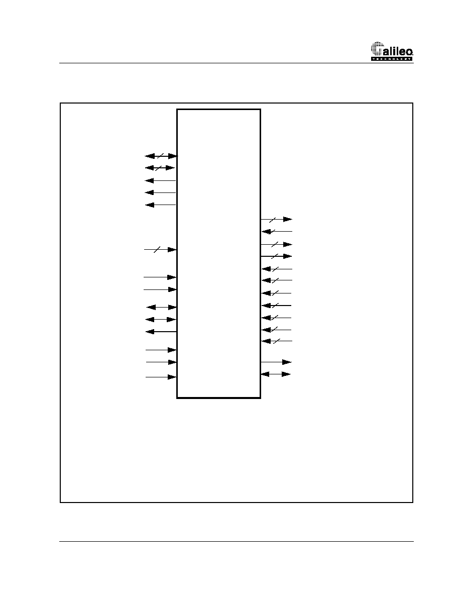
2.
Pin Information
2.1
Logic Symbol
Rst*
Clk
DData[31:0]
RAS[1:0]*
CAS*
WE*
GT-48006
DAddr[8:0]
DRAM
MII
Interface
9
LEDData
LEDStb
LEDClk
Miscellaneous
Interface
32
Scan*
TriState*
TxClk[1:0]
TxD0[3:0
]
Col[1:0]
RxD0[3:0]
RxEr[1:0]
2
2
4
2
4
2
RxClk[1:0]
RxDV[1:0]
Crs[1:0]
2
2
2
TxD1[3:0]
4
RxD1[3:0]
4
MDC
MDIO
TxEn[1:0]
Interface
Vtol
2
Aging
GT-48006A Low Cost Two Port 10/100 Ethernet Bridge/Switch Controller
4
3.
Pin Functions and Assignment
S y m b o l
Ty p e
D e s c ri p t i o n
Clock and Reset
Rst*
I
RESET: Active LOW. Rst* must be asserted for at least 10 clock cycles when
in the reset state. Following Rst* deassertion, the GT-48006A clears the inter-
nal buffers and initializes the address table in the DRAM. The address table
initialization takes 165,000 CLK cycles to complete. Any incoming packets dur-
ing address table initialization are ignored.
Clk
I
Clock: Provides the timing for the GT-48006A internal units. All functional
units except for the serial interfaces use this clock.The clock frequency is
40MHz. THIS INPUT IS NOT 5V TOLERANT.
DRAM Interface
DData[31:0]
I/O
DRAM Data: 32-bit EDO DRAM data bus. These signals connect directly to
the data input/output pins of the DRAM devices.
DAddr[8:0]
I/O
DRAM Multiplexed Address Bus: In normal operation, DAddr[8:0] contain
the DRAM multiplexed row/column address. During RESET, these multiplexed
pins are sampled by the GT-48006A to indicate various parameters as follows:
DAddr[0] - Autonegotiation enable for port 0
DAddr[1] - Autonegotiation enable for port 1
DAddr[2] - Skip Init
DAddr[3] - Limit4
DAddr[4] - VL Tag Enable passing
DAddr[5] - DRAM size
DAddr[6] - Full Duplex for port 0
DAddr[7] - Full Duplex for port 0
DAddr[8] - Back Pressure enable
RAS[1:0]*
O
Row Address Strobes: DRAM row address strobes. For the two banks.
CAS*
O
Column Address Strobe: DRAM column address strobe. The GT-48006A
always accesses 32-bit values and does not require a separate CAS* for each
byte.
WE*
O
Write Enable: DRAM write enable.
Media Independent
Interface
TxEn[1:0]
O
Transmit Enable: Active HIGH. This output indicates that the packet is being
transmitted. TxEn is synchronous to TxClk.
TxClk[1:0]
I
Transmit Clock: Provides the timing reference for the transfer of TxEn, TxD
signals. TxClk frequency is one fourth of the data rate (25 MHz for 100Mbps,
2.5 MHz for 10Mbps). TxClk nominal frequency should match the nominal fre-
quency of RxClk for the same port.
TxD0[3:0]
O
Transmit Data 0: Outputs the Port0 Transmit Data. Synchronous to TxClk[0].
TxD1[3:0]
O
Transmit Data 1: Outputs the Port1 Transmit Data. Synchronous to TxClk[1].
Col[1:0]
I
Collision detect: Active HIGH. Indicates a collision has been detected on the
wire. This input is ignored in full-duplex mode. Col is not synchronous to any
clock.
RxD0[3:0]
I
Receive Data 0: Port 0 Receive Data. Synchronous to RxClk[0].
RxD1[3:0]
I
Receive Data 1: Port 1 Receive Data. Synchronous to RxClk[1].
GT-48006A Low Cost Two Port 10/100 Ethernet Bridge/Switch Controller
5
RxEr[1:0]
I
Receive Error. Active HIGH. Indicates that an error was detected in the
received frame. This input is ignored when RxDV for the same port is inactive.
RxClK[1:0]
I
Receive Clock. Provides the timing reference for the transfer of the RxDV,
RxD, RxEr signals (per port). Operates at either 25 MHz (100Mbps) or 2.5
MHz (10Mbps). The nominal frequency of RxClk (per port) should match the
nominal frequency of that port's TxClk.
RxDV[1:0]
I
Receive Data Valid: Active HIGH. Indicates that valid data is present on the
RxD lines. Synchronous to RxClk.
CrS[1:0]
I
Carrier Sense: Active HIGH. Indicates that either the transmit or receive
medium is non-idle. CrS is not synchronous to any clock.
MDC
O
Management Data Clock: Provides the timing reference for the transfer of the
MDIO signal. This output may be connected to the PHY devices of both ports.
MDIO
I/O
Management Data Input/Output: This bidirectional line is used to transfer
control information and status between the PHY and the GT-48006A. It con-
forms with IEEE Std 802.3u. This signal may be connected to the PHY devices
of both ports. When not in use this pin must be connected to a pull-down resis-
tor.
Miscellaneous Interface Pins
LEDData I/O
LED Data/DisBufThr: In normal configuration carries the serial data bit stream
which contains the LED indicators per port. The data is shifted out using the
LEDClk. LEDStb is used to mark the first data bit. This pin is active low. During
reset, this pin is sampled by the GT-48006A for dynamic/fixed buffering alloca-
tion.
LEDStb
I/O
LED Strobe/Force Link Pass: In normal operation indicates the beginning
(data bit #1) of a valid data frame on LEDData output - active High. During
reset, this pin is sampled by the GT-48006A to Force the link to pass.
LEDClk
O
LED Clock: 1 MHz clock. This output is used to clock the LEDStb and LED-
Data outputs. During RESET, LEDClk frequency is 40 MHz.
Scan*
I
Scan: This pin together with TriState* indicate the GT-48006A mode of opera-
tion as follows:
Factory test modes are reserved and are not to be used in-system. Failure to
observe this restriction could result in damage to the device.
TriState*
I
Tri State: This pin together with Scan* indicate the GT-48006A mode of oper-
ation as described above.
S y m b o l
Ty p e
De s c ri pti o n
S c a n *
Tr i S t a t e *
M o d e
1
1
Normal operation
0
1
Factory test mode (reserved)
1
0
The GT-48006A drives all out-
puts and I/O pins to high imped-
ance.
0
0
Factory test mode (reserved)