 | –≠–ª–µ–∫—Ç—Ä–æ–Ω–Ω—ã–π –∫–æ–º–ø–æ–Ω–µ–Ω—Ç: GT-64111 | –°–∫–∞—á–∞—Ç—å:  PDF PDF  ZIP ZIP |

GT-64111
System Controller for RC4640,
RM523X and VR4300 CPUs
Product Preview
Revision 1.1
FEB 4, 1999
Please contact Galileo Technology for possible
updates before finalizing a design.
FEATURES
www.galileoT.com support@galileoT.com Tel: +1-408.367.1400 Fax: +1-408.367.1401
∑ Integrated PCI system controller for high-performance
cost sensitive embedded applications
∑ Support the following 32-bit bus CPUs:
- IDT RC4640 and RC4650 (in 32-bit mode)
- QED RM523X
-
NEC/Toshiba VR4300
∑ Up to 66MHz CPU bus frequency
∑ 64 byte CPU write posting buffer
- 32-bit wide, 16 levels deep
- Accepts CPU writes with zero wait-states
∑ EDO and Fast Page Mode DRAM controller
- 512MB address space
- Supports DRAM bank interleaving
- 256KB-16MB device depth
- 1- 4 banks supported
- 32-bit or 64-bit data width
- Parity supported
- Zero wait-state interleaved burst accesses at
66MHz
∑ Device controller
- 5 chip selects
- Programmable timing for each chip select
- Supports many types of standard memory and I/O
devices
- Up to 160MB address space
- Optional external wait-state support
- 8-,16-,32- and 64-bit width device support
- Support for boot ROMs
- Parity supported for devices
∑ Four channel DMA controller
- Chaining via linked-lists of records
- Byte alignment on source and destination
- Transfers through 32-byte internal FIFO
- Moves data between PCI, memory, and devices
∑ High-performance 32-bit Universal PCI 2.1 interface
- 96-bytes of posted write and read prefetch buffers
- 32-bit PCI master and target operations
- PCI bus speed of up to 66MHz with no wait states
- Operates either synchronous or asynchronous to
CPU clock
- Burst transfers used for efficient data movement
- Doorbell interrupts provided between CPU and PCI
- Supports flexible byte swapping through PCI inter-
face
- Synchronization barrier support
- PCI configuration registers can be accessed from
both CPU and PCI side
- Support for both 5V and 3.3V operation
∑ Host to PCI bridge
- Translates CPU cycles into PCI I/O or Memory
cycles
- Generates PCI Configuration, Interrupt Acknowl-
edge, and Special cycles on PCI bus
∑ PCI to Main Memory bridge
- Supports fast back-to-back transactions
- Supports memory and I/O transactions to internal
configuration registers
- Supports locked operations
∑ Three 24-bit wide and one 32-bit wide timer/counters
∑ Plug and Play Support
- PC compatible configuration registers
- PCI configuration header can be loaded from boot
PROM
- PCI configuration registers are accessed from both
CPU and PCI bus
∑ 3.3V Supply Voltage (PCI and Peripherals)
- 5V tolerant I/Os
∑ 208 PQFP
GT-64111
32-bit/66MHz SysAD
C P U
32-bit/66MHz PCI Bus
Network
Other
. . .
SCSI
32-bit Address/Data Bus
Address/Control
Flash
I/O
. . .
S D R A M

GT-64111 System Controller for RC4640, RM523X and VR4300 CPUs
2
Revision 1.0

GT-64111 System Controller for RC4640, RM523X and VR4300 CPUs
Revision 1.0
Table of Contents
1.
OVERVIEW.......................................................................................................................................... 7
1.1
CPU bus Interface . . . . . . . . . . . . . . . . . . . . . . . . . . . . . . . . . . . . . . . . . . . . . . . . . . . . . . . . . . . . . . . . . . . . 7
1.2
DRAM and Device Interface . . . . . . . . . . . . . . . . . . . . . . . . . . . . . . . . . . . . . . . . . . . . . . . . . . . . . . . . . . . . . 7
1.3
PCI Interface. . . . . . . . . . . . . . . . . . . . . . . . . . . . . . . . . . . . . . . . . . . . . . . . . . . . . . . . . . . . . . . . . . . . . . . . . 7
1.4
DMA Engines . . . . . . . . . . . . . . . . . . . . . . . . . . . . . . . . . . . . . . . . . . . . . . . . . . . . . . . . . . . . . . . . . . . . . . . . 8
1.5
CPUs Supported. . . . . . . . . . . . . . . . . . . . . . . . . . . . . . . . . . . . . . . . . . . . . . . . . . . . . . . . . . . . . . . . . . . . . . 8
1.6
Block Diagram . . . . . . . . . . . . . . . . . . . . . . . . . . . . . . . . . . . . . . . . . . . . . . . . . . . . . . . . . . . . . . . . . . . . . . . 8
2.
Pin Information................................................................................................................................... 10
2.1
Logic Symbol . . . . . . . . . . . . . . . . . . . . . . . . . . . . . . . . . . . . . . . . . . . . . . . . . . . . . . . . . . . . . . . . . . . . . . .10
2.2
Pin Assignment Table. . . . . . . . . . . . . . . . . . . . . . . . . . . . . . . . . . . . . . . . . . . . . . . . . . . . . . . . . . . . . . . . .11
3.
CPU/Local Master Interface .............................................................................................................. 15
3.1
CPU/Local Master Interface Signals. . . . . . . . . . . . . . . . . . . . . . . . . . . . . . . . . . . . . . . . . . . . . . . . . . . . . .15
3.2
SysAD and SysCmd Buses (9-bit SysCmd Mode) . . . . . . . . . . . . . . . . . . . . . . . . . . . . . . . . . . . . . . . . . . .15
3.2.1
SysAD Read Protocol . . . . . . . . . . . . . . . . . . . . . . . . . . . . . . . . . . . . . . . . . . . . . . . . . . . . . . . . . . . . . . 17
3.2.2
SysAD Write Protocol . . . . . . . . . . . . . . . . . . . . . . . . . . . . . . . . . . . . . . . . . . . . . . . . . . . . . . . . . . . . . . 18
3.3
4300 Bus Mode Support (5-bit SysCmd Mode) . . . . . . . . . . . . . . . . . . . . . . . . . . . . . . . . . . . . . . . . . . . . .19
3.4
Operation of WrRdy* and the Internal Write Posting Queues . . . . . . . . . . . . . . . . . . . . . . . . . . . . . . . . . .21
3.5
MIPs Write Modes and Write Patterns Supported . . . . . . . . . . . . . . . . . . . . . . . . . . . . . . . . . . . . . . . . . . .21
3.6
CPU/Local Master Interface Endianess . . . . . . . . . . . . . . . . . . . . . . . . . . . . . . . . . . . . . . . . . . . . . . . . . . .21
3.7
Burst Order . . . . . . . . . . . . . . . . . . . . . . . . . . . . . . . . . . . . . . . . . . . . . . . . . . . . . . . . . . . . . . . . . . . . . . . . .22
3.8
CPU/Local Master Interface Restrictions . . . . . . . . . . . . . . . . . . . . . . . . . . . . . . . . . . . . . . . . . . . . . . . . . .22
4.
Address Space Decoding.................................................................................................................. 23
4.1
Two Stage Decoding Process . . . . . . . . . . . . . . . . . . . . . . . . . . . . . . . . . . . . . . . . . . . . . . . . . . . . . . . . . .24
4.1.1
CPU/Local Master Side Decoding Process . . . . . . . . . . . . . . . . . . . . . . . . . . . . . . . . . . . . . . . . . . . . . 25
4.2
PCI Side Decoding Process . . . . . . . . . . . . . . . . . . . . . . . . . . . . . . . . . . . . . . . . . . . . . . . . . . . . . . . . . . . .28
4.3
Disabling the Device Decoders . . . . . . . . . . . . . . . . . . . . . . . . . . . . . . . . . . . . . . . . . . . . . . . . . . . . . . . . .28
4.4
DMA Unit Address Decoding . . . . . . . . . . . . . . . . . . . . . . . . . . . . . . . . . . . . . . . . . . . . . . . . . . . . . . . . . . .28
4.5
Address Space Decoding Errors . . . . . . . . . . . . . . . . . . . . . . . . . . . . . . . . . . . . . . . . . . . . . . . . . . . . . . . .29
4.6
Default Memory Map . . . . . . . . . . . . . . . . . . . . . . . . . . . . . . . . . . . . . . . . . . . . . . . . . . . . . . . . . . . . . . . . .29
5.
Memory Controller ............................................................................................................................. 31
5.1
DRAM Controller . . . . . . . . . . . . . . . . . . . . . . . . . . . . . . . . . . . . . . . . . . . . . . . . . . . . . . . . . . . . . . . . . . . .31
5.1.1
DRAM Refresh . . . . . . . . . . . . . . . . . . . . . . . . . . . . . . . . . . . . . . . . . . . . . . . . . . . . . . . . . . . . . . . . . . . 31
5.1.2
Assymetrically RAS*/CAS* Addressing . . . . . . . . . . . . . . . . . . . . . . . . . . . . . . . . . . . . . . . . . . . . . . . . 32
5.1.3
DAdr[11]/ADS* Function . . . . . . . . . . . . . . . . . . . . . . . . . . . . . . . . . . . . . . . . . . . . . . . . . . . . . . . . . . . . 33
5.1.4
Programmable DRAM Timing Parameters . . . . . . . . . . . . . . . . . . . . . . . . . . . . . . . . . . . . . . . . . . . . . . 33
5.1.5
DRAM Bank Width and Location . . . . . . . . . . . . . . . . . . . . . . . . . . . . . . . . . . . . . . . . . . . . . . . . . . . . . 34
5.1.6
DRAM Performance . . . . . . . . . . . . . . . . . . . . . . . . . . . . . . . . . . . . . . . . . . . . . . . . . . . . . . . . . . . . . . . 34
5.2
Device Controller . . . . . . . . . . . . . . . . . . . . . . . . . . . . . . . . . . . . . . . . . . . . . . . . . . . . . . . . . . . . . . . . . . . .35
5.2.1
TurnOff, bits [2:0] . . . . . . . . . . . . . . . . . . . . . . . . . . . . . . . . . . . . . . . . . . . . . . . . . . . . . . . . . . . . . . . . . 35
5.2.2
AccToFirst, bits [6:3] . . . . . . . . . . . . . . . . . . . . . . . . . . . . . . . . . . . . . . . . . . . . . . . . . . . . . . . . . . . . . . . 35
5.2.3
AccToNext, bits [10:7]. . . . . . . . . . . . . . . . . . . . . . . . . . . . . . . . . . . . . . . . . . . . . . . . . . . . . . . . . . . . . . 35
5.2.4
ADStoWr, bits[13:11] . . . . . . . . . . . . . . . . . . . . . . . . . . . . . . . . . . . . . . . . . . . . . . . . . . . . . . . . . . . . . . 36
5.2.5
WrActive, bits[16:14] . . . . . . . . . . . . . . . . . . . . . . . . . . . . . . . . . . . . . . . . . . . . . . . . . . . . . . . . . . . . . . . 36
5.2.6
WrHigh, bits[19:17] . . . . . . . . . . . . . . . . . . . . . . . . . . . . . . . . . . . . . . . . . . . . . . . . . . . . . . . . . . . . . . . . 36
5.2.7
Burst Transactions . . . . . . . . . . . . . . . . . . . . . . . . . . . . . . . . . . . . . . . . . . . . . . . . . . . . . . . . . . . . . . . . 39
5.2.8
Packing and Unpacking Data and Burst Support . . . . . . . . . . . . . . . . . . . . . . . . . . . . . . . . . . . . . . . . . 39
5.2.9
"Destructive" Reads . . . . . . . . . . . . . . . . . . . . . . . . . . . . . . . . . . . . . . . . . . . . . . . . . . . . . . . . . . . . . . . 39
5.2.10
Ready* Support. . . . . . . . . . . . . . . . . . . . . . . . . . . . . . . . . . . . . . . . . . . . . . . . . . . . . . . . . . . . . . . . . . . 40
5.2.11
Device Bank Width and Location . . . . . . . . . . . . . . . . . . . . . . . . . . . . . . . . . . . . . . . . . . . . . . . . . . . . . 43

GT-64111 System Controller for RC4640, RM523X and VR4300 CPUs
4
Revision 1.0
5.2.12
SysAD to AD Addressing. . . . . . . . . . . . . . . . . . . . . . . . . . . . . . . . . . . . . . . . . . . . . . . . . . . . . . . . . . . . 43
5.3
Data Latches . . . . . . . . . . . . . . . . . . . . . . . . . . . . . . . . . . . . . . . . . . . . . . . . . . . . . . . . . . . . . . . . . . . . . . . 44
5.3.1
Enabling Latch Control Signals on Read Transactions . . . . . . . . . . . . . . . . . . . . . . . . . . . . . . . . . . . . . 44
5.4
Parity Checking Support . . . . . . . . . . . . . . . . . . . . . . . . . . . . . . . . . . . . . . . . . . . . . . . . . . . . . . . . . . . . . . 44
5.5
Addressing . . . . . . . . . . . . . . . . . . . . . . . . . . . . . . . . . . . . . . . . . . . . . . . . . . . . . . . . . . . . . . . . . . . . . . . . 45
5.6
Memory Interface Restrictions . . . . . . . . . . . . . . . . . . . . . . . . . . . . . . . . . . . . . . . . . . . . . . . . . . . . . . . . . 45
6.
PCI Bus ............................................................................................................................................... 47
6.1
PCI Master Operation . . . . . . . . . . . . . . . . . . . . . . . . . . . . . . . . . . . . . . . . . . . . . . . . . . . . . . . . . . . . . . . . 47
6.1.1
PCI Master CPU/Local Master Address Space Decode and Translation . . . . . . . . . . . . . . . . . . . . . . . 47
6.1.2
PCI Master CPU/Local Master Byte Swapping . . . . . . . . . . . . . . . . . . . . . . . . . . . . . . . . . . . . . . . . . . . 47
6.1.3
PCI Master FIFOs . . . . . . . . . . . . . . . . . . . . . . . . . . . . . . . . . . . . . . . . . . . . . . . . . . . . . . . . . . . . . . . . . 47
6.1.4
PCI Master DMA . . . . . . . . . . . . . . . . . . . . . . . . . . . . . . . . . . . . . . . . . . . . . . . . . . . . . . . . . . . . . . . . . . 48
6.1.5
PCI Master RETRY Counter . . . . . . . . . . . . . . . . . . . . . . . . . . . . . . . . . . . . . . . . . . . . . . . . . . . . . . . . . 48
6.1.6
Cache Line Size. . . . . . . . . . . . . . . . . . . . . . . . . . . . . . . . . . . . . . . . . . . . . . . . . . . . . . . . . . . . . . . . . . . 48
6.2
PCI Target Interface . . . . . . . . . . . . . . . . . . . . . . . . . . . . . . . . . . . . . . . . . . . . . . . . . . . . . . . . . . . . . . . . . 48
6.2.1
PCI Target FIFOs . . . . . . . . . . . . . . . . . . . . . . . . . . . . . . . . . . . . . . . . . . . . . . . . . . . . . . . . . . . . . . . . . 49
6.2.2
PCI Target Address Space Decode and Byte Swapping. . . . . . . . . . . . . . . . . . . . . . . . . . . . . . . . . . . . 50
6.2.3
Tweaking the Performance of the Target Interface . . . . . . . . . . . . . . . . . . . . . . . . . . . . . . . . . . . . . . . . 51
6.3
PCI Synchronization Barriers . . . . . . . . . . . . . . . . . . . . . . . . . . . . . . . . . . . . . . . . . . . . . . . . . . . . . . . . . . 51
6.4
PCI Master Configuration . . . . . . . . . . . . . . . . . . . . . . . . . . . . . . . . . . . . . . . . . . . . . . . . . . . . . . . . . . . . . 51
6.4.1
Special Cycles and Interrupt Acknowledge . . . . . . . . . . . . . . . . . . . . . . . . . . . . . . . . . . . . . . . . . . . . . . 52
6.5
Target Configuration and Plug and Play . . . . . . . . . . . . . . . . . . . . . . . . . . . . . . . . . . . . . . . . . . . . . . . . . . 52
6.5.1
Plug and Play Base Address Register Sizing . . . . . . . . . . . . . . . . . . . . . . . . . . . . . . . . . . . . . . . . . . . . 52
6.5.2
Multi-Function Device, Swap BARs . . . . . . . . . . . . . . . . . . . . . . . . . . . . . . . . . . . . . . . . . . . . . . . . . . . . 53
6.5.3
PCI Autoconfiguration at RESET. . . . . . . . . . . . . . . . . . . . . . . . . . . . . . . . . . . . . . . . . . . . . . . . . . . . . . 53
6.5.4
Expansion ROM Functionality . . . . . . . . . . . . . . . . . . . . . . . . . . . . . . . . . . . . . . . . . . . . . . . . . . . . . . . . 54
6.6
PCI Parity Support . . . . . . . . . . . . . . . . . . . . . . . . . . . . . . . . . . . . . . . . . . . . . . . . . . . . . . . . . . . . . . . . . . 54
6.7
PCI Bus/Device Bus/CPU/Local Master Clock Synchronization . . . . . . . . . . . . . . . . . . . . . . . . . . . . . . . . 55
6.8
66MHz Capability Bit. . . . . . . . . . . . . . . . . . . . . . . . . . . . . . . . . . . . . . . . . . . . . . . . . . . . . . . . . . . . . . . . . 55
6.9
Universal PCI Vio Pin . . . . . . . . . . . . . . . . . . . . . . . . . . . . . . . . . . . . . . . . . . . . . . . . . . . . . . . . . . . . . . . . 55
6.10 PCI Interface Restrictions . . . . . . . . . . . . . . . . . . . . . . . . . . . . . . . . . . . . . . . . . . . . . . . . . . . . . . . . . . . . . 55
6.10.1
Master . . . . . . . . . . . . . . . . . . . . . . . . . . . . . . . . . . . . . . . . . . . . . . . . . . . . . . . . . . . . . . . . . . . . . . . . . . 55
6.10.2
Slave . . . . . . . . . . . . . . . . . . . . . . . . . . . . . . . . . . . . . . . . . . . . . . . . . . . . . . . . . . . . . . . . . . . . . . . . . . . 55
6.10.3
Master and Slave. . . . . . . . . . . . . . . . . . . . . . . . . . . . . . . . . . . . . . . . . . . . . . . . . . . . . . . . . . . . . . . . . . 55
7.
DMA Controller .................................................................................................................................. 56
7.1
DMA Channel Registers . . . . . . . . . . . . . . . . . . . . . . . . . . . . . . . . . . . . . . . . . . . . . . . . . . . . . . . . . . . . . . 57
7.2
DMA Channel Control Register (0x840 - 0x84c). . . . . . . . . . . . . . . . . . . . . . . . . . . . . . . . . . . . . . . . . . . . 57
7.2.1
AddControl[1:0], GT-64111-P-1 ONLY . . . . . . . . . . . . . . . . . . . . . . . . . . . . . . . . . . . . . . . . . . . . . . . . . 57
7.2.2
SrcDir, bits[3:2] . . . . . . . . . . . . . . . . . . . . . . . . . . . . . . . . . . . . . . . . . . . . . . . . . . . . . . . . . . . . . . . . . . . 57
7.2.3
DestDir, bits[5:4] . . . . . . . . . . . . . . . . . . . . . . . . . . . . . . . . . . . . . . . . . . . . . . . . . . . . . . . . . . . . . . . . . . 57
7.2.4
DatTransLim, bits[8:6] . . . . . . . . . . . . . . . . . . . . . . . . . . . . . . . . . . . . . . . . . . . . . . . . . . . . . . . . . . . . . . 58
7.2.5
ChainMod, bit 9 . . . . . . . . . . . . . . . . . . . . . . . . . . . . . . . . . . . . . . . . . . . . . . . . . . . . . . . . . . . . . . . . . . . 58
7.2.6
IntMode, bit 10 . . . . . . . . . . . . . . . . . . . . . . . . . . . . . . . . . . . . . . . . . . . . . . . . . . . . . . . . . . . . . . . . . . . . 58
7.2.7
TransMod, bit 11 . . . . . . . . . . . . . . . . . . . . . . . . . . . . . . . . . . . . . . . . . . . . . . . . . . . . . . . . . . . . . . . . . . 59
7.2.8
ChanEn, bit 12 . . . . . . . . . . . . . . . . . . . . . . . . . . . . . . . . . . . . . . . . . . . . . . . . . . . . . . . . . . . . . . . . . . . . 59
7.2.9
FetNexRec, bit 13 . . . . . . . . . . . . . . . . . . . . . . . . . . . . . . . . . . . . . . . . . . . . . . . . . . . . . . . . . . . . . . . . . 59
7.2.10
DMAActSt, bit 14 (Read Only) . . . . . . . . . . . . . . . . . . . . . . . . . . . . . . . . . . . . . . . . . . . . . . . . . . . . . . . . 59
7.3
Restarting a Disabled Channel (previously active) . . . . . . . . . . . . . . . . . . . . . . . . . . . . . . . . . . . . . . . . . . 59
7.4
Reprogramming an Active Channel . . . . . . . . . . . . . . . . . . . . . . . . . . . . . . . . . . . . . . . . . . . . . . . . . . . . . 60
7.5
Arbitration . . . . . . . . . . . . . . . . . . . . . . . . . . . . . . . . . . . . . . . . . . . . . . . . . . . . . . . . . . . . . . . . . . . . . . . . . 60
7.6
DMAReq[3:0]* . . . . . . . . . . . . . . . . . . . . . . . . . . . . . . . . . . . . . . . . . . . . . . . . . . . . . . . . . . . . . . . . . . . . . . 60
7.7
DMAAck[3:0]* . . . . . . . . . . . . . . . . . . . . . . . . . . . . . . . . . . . . . . . . . . . . . . . . . . . . . . . . . . . . . . . . . . . . . . 61
7.8
Design Information . . . . . . . . . . . . . . . . . . . . . . . . . . . . . . . . . . . . . . . . . . . . . . . . . . . . . . . . . . . . . . . . . . 61
7.8.1
DMA in Demand Mode . . . . . . . . . . . . . . . . . . . . . . . . . . . . . . . . . . . . . . . . . . . . . . . . . . . . . . . . . . . . . 61

GT-64111 System Controller for RC4640, RM523X and VR4300 CPUs
Revision 1.0
7.8.2
DMA in Block Mode . . . . . . . . . . . . . . . . . . . . . . . . . . . . . . . . . . . . . . . . . . . . . . . . . . . . . . . . . . . . . . . 62
7.8.3
Non-Chain Mode. . . . . . . . . . . . . . . . . . . . . . . . . . . . . . . . . . . . . . . . . . . . . . . . . . . . . . . . . . . . . . . . . . 62
7.8.4
Chain Mode. . . . . . . . . . . . . . . . . . . . . . . . . . . . . . . . . . . . . . . . . . . . . . . . . . . . . . . . . . . . . . . . . . . . . . 62
7.8.5
Dynamic DMA chaining . . . . . . . . . . . . . . . . . . . . . . . . . . . . . . . . . . . . . . . . . . . . . . . . . . . . . . . . . . . . 62
7.9
DMA Restrictions . . . . . . . . . . . . . . . . . . . . . . . . . . . . . . . . . . . . . . . . . . . . . . . . . . . . . . . . . . . . . . . . . . . .62
8.
Timer/Counters .................................................................................................................................. 64
9.
Interrupt Controller ............................................................................................................................ 65
10.
Reset Configuration........................................................................................................................... 66
11.
Connecting the Memory Controller to DRAM and Devices............................................................ 69
11.1 Working Without Data Latches . . . . . . . . . . . . . . . . . . . . . . . . . . . . . . . . . . . . . . . . . . . . . . . . . . . . . . . . . .69
11.2 Working With Data Latches . . . . . . . . . . . . . . . . . . . . . . . . . . . . . . . . . . . . . . . . . . . . . . . . . . . . . . . . . . . .70
11.2.1
64-bit DRAM . . . . . . . . . . . . . . . . . . . . . . . . . . . . . . . . . . . . . . . . . . . . . . . . . . . . . . . . . . . . . . . . . . . . . 70
11.2.2
32-bit DRAM . . . . . . . . . . . . . . . . . . . . . . . . . . . . . . . . . . . . . . . . . . . . . . . . . . . . . . . . . . . . . . . . . . . . . 71
11.2.3
64-bit Devices . . . . . . . . . . . . . . . . . . . . . . . . . . . . . . . . . . . . . . . . . . . . . . . . . . . . . . . . . . . . . . . . . . . . 72
11.2.4
32-bit or Less Devices . . . . . . . . . . . . . . . . . . . . . . . . . . . . . . . . . . . . . . . . . . . . . . . . . . . . . . . . . . . . . 73
12.
Big and Little Endian ......................................................................................................................... 74
12.1 Background . . . . . . . . . . . . . . . . . . . . . . . . . . . . . . . . . . . . . . . . . . . . . . . . . . . . . . . . . . . . . . . . . . . . . . . .74
12.1.1
Bit 12 of the CPU/Local Master Interface Configuration register . . . . . . . . . . . . . . . . . . . . . . . . . . . . . 74
12.1.2
Bit 0 of the PCI Internal Command register . . . . . . . . . . . . . . . . . . . . . . . . . . . . . . . . . . . . . . . . . . . . . 74
12.2 Configuring a System for Big and Little Endian . . . . . . . . . . . . . . . . . . . . . . . . . . . . . . . . . . . . . . . . . . . . .74
13.
Using the GT-64111 Without the CPU/Local Master Interface ....................................................... 76
14.
Using the GT-64111 Without the PCI Interface................................................................................ 76
15.
APPLICATIONS: SYSTEM CONFIGURATIONS ............................................................................... 77
15.1 Minimal System Configuration . . . . . . . . . . . . . . . . . . . . . . . . . . . . . . . . . . . . . . . . . . . . . . . . . . . . . . . . . .77
15.2 Typical System . . . . . . . . . . . . . . . . . . . . . . . . . . . . . . . . . . . . . . . . . . . . . . . . . . . . . . . . . . . . . . . . . . . . . .78
15.3 Interface to Asynchronous Devices . . . . . . . . . . . . . . . . . . . . . . . . . . . . . . . . . . . . . . . . . . . . . . . . . . . . . .79
15.4 Interface to DRAM . . . . . . . . . . . . . . . . . . . . . . . . . . . . . . . . . . . . . . . . . . . . . . . . . . . . . . . . . . . . . . . . . . .80
15.5 A System With Parity . . . . . . . . . . . . . . . . . . . . . . . . . . . . . . . . . . . . . . . . . . . . . . . . . . . . . . . . . . . . . . . . .81
16.
Designing for Compatibility with the GT-64011 .............................................................................. 83
16.1 Major Hardware Differences Between the GT-64011 and GT-64111 . . . . . . . . . . . . . . . . . . . . . . . . . . . .83
16.2 All Differences Between the GT-64011 and GT-64111 . . . . . . . . . . . . . . . . . . . . . . . . . . . . . . . . . . . . . . .83
17.
REGISTER TABLES ........................................................................................................................... 85
17.1 Access to On-Chip PCI Configuration Space Registers . . . . . . . . . . . . . . . . . . . . . . . . . . . . . . . . . . . . . . .85
17.2 Register Map . . . . . . . . . . . . . . . . . . . . . . . . . . . . . . . . . . . . . . . . . . . . . . . . . . . . . . . . . . . . . . . . . . . . . . .85
17.3 CPU/Local Master Interface . . . . . . . . . . . . . . . . . . . . . . . . . . . . . . . . . . . . . . . . . . . . . . . . . . . . . . . . . . . .90
17.4 CPU/Local Master Decode . . . . . . . . . . . . . . . . . . . . . . . . . . . . . . . . . . . . . . . . . . . . . . . . . . . . . . . . . . . . .90
17.5 Device Decode . . . . . . . . . . . . . . . . . . . . . . . . . . . . . . . . . . . . . . . . . . . . . . . . . . . . . . . . . . . . . . . . . . . . . .93
17.6 DRAM Configuration. . . . . . . . . . . . . . . . . . . . . . . . . . . . . . . . . . . . . . . . . . . . . . . . . . . . . . . . . . . . . . . . . .96
17.7 DRAM Parameters . . . . . . . . . . . . . . . . . . . . . . . . . . . . . . . . . . . . . . . . . . . . . . . . . . . . . . . . . . . . . . . . . . .96
17.8 Device Parameters . . . . . . . . . . . . . . . . . . . . . . . . . . . . . . . . . . . . . . . . . . . . . . . . . . . . . . . . . . . . . . . . . . .98
17.9 DMA Record . . . . . . . . . . . . . . . . . . . . . . . . . . . . . . . . . . . . . . . . . . . . . . . . . . . . . . . . . . . . . . . . . . . . .99
17.10 DMA Channel Control. . . . . . . . . . . . . . . . . . . . . . . . . . . . . . . . . . . . . . . . . . . . . . . . . . . . . . . . . . . . . . . .102
17.11 Arbiter Control, Offset: 0x860 . . . . . . . . . . . . . . . . . . . . . . . . . . . . . . . . . . . . . . . . . . . . . . . . . . . . . . . . . .104
17.12 Timer / Counter. . . . . . . . . . . . . . . . . . . . . . . . . . . . . . . . . . . . . . . . . . . . . . . . . . . . . . . . . . . . . . . . . . . . .104
17.13 PCI Internal. . . . . . . . . . . . . . . . . . . . . . . . . . . . . . . . . . . . . . . . . . . . . . . . . . . . . . . . . . . . . . . . . . . . . . . .106
17.14 Interrupts . . . . . . . . . . . . . . . . . . . . . . . . . . . . . . . . . . . . . . . . . . . . . . . . . . . . . . . . . . . . . . . . . . . . . . . . .110
17.15 PCI Configuration Registers . . . . . . . . . . . . . . . . . . . . . . . . . . . . . . . . . . . . . . . . . . . . . . . . . . . . . . . . . . .112
17.15.1 FUNCTION 1 CONFIGURATION REGISTERS . . . . . . . . . . . . . . . . . . . . . . . . . . . . . . . . . . . . . . . . . 115

GT-64111 System Controller for RC4640, RM523X and VR4300 CPUs
6
Revision 1.0
18.
PINOUT TABLE, 208 pin PQFP (sorted by number)..................................................................... 117
19.
DC CHARACTERISTICS - PRELIMINARY/SUBJECT TO CHANGE .............................................. 119
19.1 Absolute Maximum Ratings . . . . . . . . . . . . . . . . . . . . . . . . . . . . . . . . . . . . . . . . . . . . . . . . . . . . . . . . . . 119
19.2 Recommended Operating Conditions . . . . . . . . . . . . . . . . . . . . . . . . . . . . . . . . . . . . . . . . . . . . . . . . . . . 119
19.3 DC Electrical Characteristics Over Operating Range . . . . . . . . . . . . . . . . . . . . . . . . . . . . . . . . . . . . . . . 119
19.4 Thermal Data . . . . . . . . . . . . . . . . . . . . . . . . . . . . . . . . . . . . . . . . . . . . . . . . . . . . . . . . . . . . . . . . . . . . . 121
20.
AC TIMING - TARGETS/SUBJECT TO CHANGE ........................................................................... 122
20.1 TClk/PClk Restrictions . . . . . . . . . . . . . . . . . . . . . . . . . . . . . . . . . . . . . . . . . . . . . . . . . . . . . . . . . . . . . . 123
21.
Functional Waveforms .................................................................................................................... 128
22.
Packaging ......................................................................................................................................... 129
23.
Revision History .............................................................................................................................. 130

GT-64111 System Controller for RC4640, RM523X and VR4300 CPUs
Revision 1.0
1.
OVERVIEW
The GT-64111 provides a single-chip solution for designers building systems around 32-bit bus/64-bit internal MIPS
embedded processors. The architecture of the GT-64111 supports several system implementations for different appli-
cations and cost/performance points. It is possible to design a powerful system with minimal glue logic, or add com-
modity logic (controlled by the GT-64111) for differentiated system architectures that attain higher performance.
The GT-64111 has a three bus architecture:
∑
A 32-bit interface to the CPU bus (SysAD bus)
∑
A 32-bit interface to the memory and device subsystem.
∑
A 32-bit interface to the PCI bus.
The three buses are de-coupled from each other in most accesses, enabling concurrent operation of the CPU bus, PCI
devices, and accesses to memory. For example, the CPU bus can write to the on-chip write buffer, a DMA agent can
move data from DRAM to its own buffers, and a PCI device can write into an on-chip FIFO, all simultaneously.
1.1
CPU bus Interface
The GT-64111 SysAD bus allows the CPU and other local bus masters to access the PCI and memory/device buses.
The SysAD bus protocol supports byte and 32-bit word operations with burst lengths up to 8 words (sub-word, 2 word,
and 4 word transfers are also supported.) With a maximum frequency of 66MHz, the CPU can transfer in excess of 150
Mbytes/sec.
The GT-64111 can automatically determine if the attached MIPS processor is using the 8-bit SysCmd protocol
(RC4640, RM523X) or the 5-bit SysCmd protocol (VR4300).
1.2
DRAM and Device Interface
The GT-64111 has a flexible DRAM controller that supports EDO as well as standard page mode DRAMs. With 45ns
standard DRAMs, the GT-64111 can return data at
8-2-2-2-2-2-2-2
1
clocks with 32-bit DRAMs and at 8-1-1-1-1-1-1-1
clocks with 64-bit interleaved DRAMs to the CPU bus- at 66Mhz local bus speed. (In "wait-state" nomenclature this
equates to 5-1-1-1-1-1-1-1 and 5-0-0-0-0-0-0-0.) The DRAM controller supports different depth devices in each bank.
NOTE: The performance acheived in interleave mode is equivalent to that possible with SDRAM. Furthermore, EDO
does not have the granularity/memory waste issues associated with SDRAM (i.e. it is easy to build the smaller arrays
required in many systems.)
The GT-64111 memory controller supports different types of memory and I/O devices. It has the control signals and the
timing programmability to support devices such as Flash, EPROMs, SRAMs, FIFOs, and I/O controllers. Device widths
from 8-bits to 64-bits are supported.
Parity generation and checking is supported externally and is optional for each bank of DRAM or any other device on
the memory bus.
1.3
PCI Interface
The GT-64111 interfaces directly with the PCI bus. The GT-64111 can be either a master initiating a PCI bus operation,
or a target responding to a PCI bus operation. The GT-64111 incorporates 96-bytes of posted write and read prefetch
buffers for efficient data transfer between the CPU bus/DMA to PCI, and PCI to main memory.
The GT-64111 becomes a PCI bus master when the CPU bus or the internal DMA engine initiates a bus cycle to a PCI
device. The following PCI bus cycles are supported: Memory Read/Write, Interrupt Acknowledge, Special, I/O Read/
Write, or Configuration Read/Write.
The GT-64111 acts as a target when a PCI device initiates a memory access (or an I/O access in the case of internal
registers). It responds to all memory read/write accesses, as well as to all configuration and I/O cycles in the case of
internal registers.
The GT-64111 contains the required PCI configuration registers. All internal registers, including the PCI configuration
1. Note that Galileo uses "total clock" nomenclature and not "wait-state" nomenclature. This means that 8-1-1-1... means 8 clocks to the
first data, 1 clock for each additional data (zero wait-states).

GT-64111 System Controller for RC4640, RM523X and VR4300 CPUs
8
Revision 1.0
registers, can be accessed from both the CPU bus and the PCI bus. The GT-64111 configuration register set is PC
Plug and Play compatible.
The PCI interface can operate up to 66MHz and is Universal PCI compatible (3.3V/5V).
1.4
DMA Engines
The GT-64111 incorporates four high performance DMA engines. Each DMA engine has the capability to transfer data
between PCI devices, between PCI devices and main memory, or between devices residing on the device/memory
bus. The DMA uses an internal 32-byte FIFO for temporary storage of DMA data. Source and destination addresses
can be non-aligned on any byte address boundary. The DMA channels can be programmed by the CPU bus or by PCI
masters, or without CPU bus intervention via a linked list of records that is loaded by the DMA controller into the chan-
nel's working set when a DMA transaction ends. The DMA supports increment/decrement/hold on source and destina-
tion addresses independently.
1.5
CPUs Supported
The GT-64111 can be used with the following processors:
∑
Integrated Device Technology's (www.idt.com) RC4640 and RC4650 (in 32-bit bus mode)
∑
Quantum Effect Design's (www.qedinc.com) RM523X
∑
NEC and Toshiba VR4300
1.6
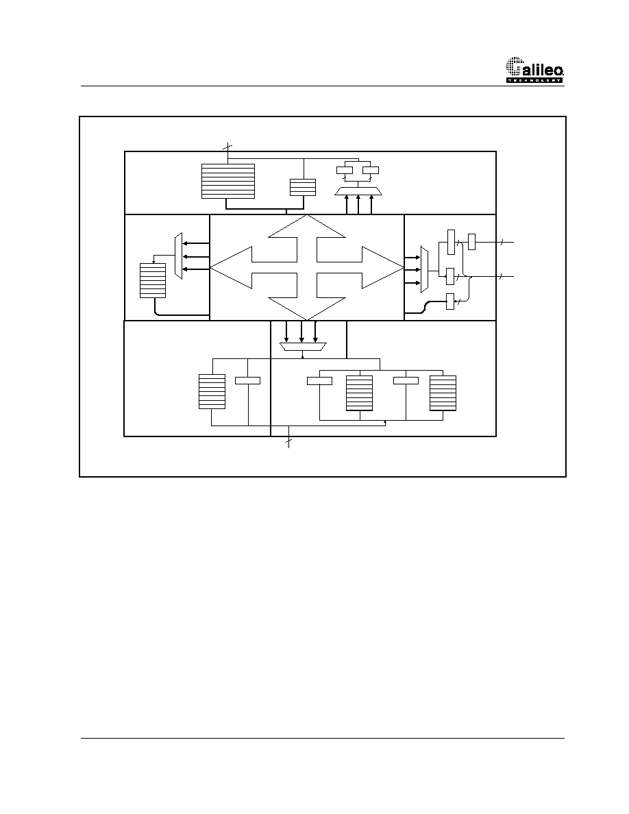
Block Diagram
Figure 1, below, shows a simplified block diagram of the GT-64111.
GT-64111 System Controller for RC4640, RM523X and VR4300 CPUs
Revision 1.0
Figure 1: GT-64111 Internal Block Diagram
Address
Data
Data
Address
Address
16 x 32
Write
Buffer
MUX
M
U
X
M
U
X
MUX
4x32
Address
Buffer
8x32
FIFO
8x32
FIFO
8x32
FIFO
8x32
FIFO
Address
Data
Data
Processor Unit
DMA Unit
Memory Unit
PCI Slave
PCI Master
DAdr
AD
SysAD
32
32
32
DRAM
Control
12
32
32
32
32
32
PCI AD
Inter-Unit Buses
GT-64111 System Controller for RC4640, RM523X and VR4300 CPUs
10
Revision 1.0
2.
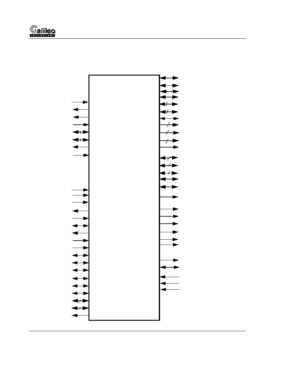
Pin Information
2.1
Logic Symbol
ValidOut*
ValidIn*
WrRdy*
Release*
SysAD
SysCmd[8:0]
[31:0]
TClk
Interrupt*
Rst*
PClk
Req*
Gnt*
PErr*
SErr*
Lock*
DevSel*
Stop*
Frame*
Par
TRdy*
IRdy*
PAD[31:0]
CBE[3:0]*
DWr*
RAS[3:0]*
AD[31:28]/CS[3:0]*
OEO*
OEE*
OEB
ALE
IdSel
ECAS[3:0]*
OCAS[3:0]*
LEO
DRAM
DMA
PCI
Interface
CPU/Local
Interface
32
4
32
9
Int*
DAdr[6:4]/EWr[3:1]*
DAdr[10:7]/OWr[3:0]*
AD[27:24]/DMAAck[3:0]*
4
22
CSTiming*
LEE
LEAdrO
DMAReq[3]*
DMAReq[1]*/ParErr*
3
4
4
4
DAdr[11]/ADS*
AD[23:2]
Local
Device
Bus
Latch
Control
GT-64111
AD[0]/BootCS*
AD[1]/ DevRW*
LEAdrE/DMAReq[2]*
DAdr[0]/BAdr[0]
4
4
&
Devices
DMAReq[0]*/Ready*
DAdr[1]/BAdr[1]
DAdr[2]/BAdr[2]
DAdr[3]/EWr[0]
Master
Vio

GT-64111 System Controller for RC4640, RM523X and VR4300 CPUs
Revision 1.0
2.2
Pin Assignment Table
Pin Name
I/O
Description
CPU/Local Master Interface
Release*
I
Release Interface: Signals to the GT-64111 that the CPU/Local Master has released
the SysAD and SysCmd buses for completion of a read request.
WrRdy*
O
Write Ready: The GT-64111 signals that it can accept a CPU/Local Master write
request (i.e. there is room in the write posting FIFO.)
ValidIn*
O
Valid Input: The GT-64111 signals that it is driving valid data on the SysAD bus, and a
valid data identifier on the SysCmd bus.
ValidOut*
I
Valid Output: Signals that the CPU/Local Master is driving valid address or data on the
SysAD bus and a valid command or data identifier on the SysCmd bus.
SysAD[31:0]
I/O
System Address/Data Bus: A 32-bit address and data bus for communication
between the CPU/Local Master and GT-64111.
SysCmd[8:0]
I/O
System Command/Data Identifier Bus: A 9-bit bus for command and data identifier
transmission between the CPU/Local Master and GT-64111. Only bits SysCmd[4:0] are
used when supporting the 4300 bus protocol.
Interrupt*
I/O
Interrupt: An "OR" of all the internal interrupt sources on the GT-64111. This pin is also
sampled as an input at reset for configuration purposes.
TClk
I
Clock: The input clock to the GT-64111 (up to 66MHz). TClk is used for both the SysAD
and Device interface. TClk must be driven for all applications, including those that do
not use the CPU/Local Master bus.
PCI Interface
PClk
I
PCI Clock: This pin provides the timing for the PCI transactions. The PCI clock range is
between 0 and 66MHz. The PClk frequency must be lower than TClk by at least 1
MHz. Please see AC Timing Specifications for more information.
Rst*
I
Reset: Resets the GT-64111 to its initial state. This signal must be asserted for at least
10 PCI clock cycles. When in the reset state, all PCI output pins are put into tristate and
all open drain signals are floated.
PAD[31:0]
I/O
PCI Address/Data: 32-bit multiplexed PCI address and data lines. During the first clock
of the transaction, PAD[31:0] contains a physical byte address (32 bits). During subse-
quent clock cycles, PAD[31:0] contains data.
CBE[3:0]*
I/O
PCI Bus Command/Byte Enable: During the address phase of the transaction,
CBE[3:0]* provide the PCI bus command. During the data phase, these lines provide
the byte enables.
Par
I/O
Parity: Calculated by the GT-64111 as an even parity bit for the PAD[31:0] and
CBE[3:0]* lines.
Frame*
I/O
Frame: Asserted by the GT-64111 to indicate the beginning and duration of a master
transaction. Frame* asserts to indicate the beginning of the cycle. While Frame* is
asserted, data transfer continues. Frame* deasserts to indicate that the next data
phase is the final data phase transaction. Frame* is monitored by the GT-64111 when it
acts as a target.
IRdy*
I/O
Initiator Ready: Indicates the bus master's ability to complete the current data phase
of the transaction. A data phase is completed on any clock when both TRdy* and IRdy*
are asserted. Wait cycles are inserted until TRdy* and IRdy* are asserted together.
TRdy*
I/O
Target Ready: Indicates the target agent's ability to complete the current data phase
of the transaction. A data phase is completed on any clock when both TRdy* and IRdy*
are asserted. Wait cycles are inserted until TRdy* and IRdy* are asserted together.

GT-64111 System Controller for RC4640, RM523X and VR4300 CPUs
12
Revision 1.0
Stop*
I/O
Stop: Indicates that the current target is requesting the bus master to stop the current
transaction. As a master, the GT-64111 responds to the assertion of Stop* by discon-
necting, retrying or aborting. As a target, the GT-64111 asserts Stop* to retry or discon-
nect.
Lock*
I
Lock: Indicates an atomic operation that may require multiple transactions to complete.
When the GT-64111 is a PCI target, Lock* is sampled on the rising edge of the PClk
when Frame* is asserted. If Lock* is sampled asserted, the GT-64111 enters into a
locked state and remains in this state until Lock* is sampled deasserted on the follow-
ing rising edge of PClk, when Frame* is sampled asserted.
IdSel
I
Initialization Device Select: Asserted to act as a chip select during PCI configuration
read and write transactions.
DevSel*
I/O
Device Select: Asserted by the target of the current access. When the GT-64111 is bus
master, it expects the target to assert DevSel* within 5 bus cycles, confirming the
access. If the target does not assert DevSel* within the required bus cycles, the GT-
64111 aborts the cycle. As a target, when the GT-64111 recognizes its transaction, it
asserts DevSel* in a medium speed (two cycles after the assertion of Frame*).
Req*
O
Bus Request: Asserted by the GT-64111 to indicate to the PCI bus arbiter that it
requires use of the PCI bus.
Gnt*
I
Bus Grant: Indicates to the GT-64111 that access to the PCI bus is granted.
PErr*
I/O
Parity Error: Asserted when a data parity error is detected.
SErr*
O
System Error: Asserted when a serious system error (not necessarily a PCI error) is
detected. The GT-64111 asserts the SErr* two cycles after the failing address. This out-
put features an open-drain driver.
Int*
O
Interrupt Request:Asserted by the GT-64111 when one of the unmasked internal inter-
rupt sources is asserted. This output features an open-drain driver.
Vio
I
PCI Voltage Sense: This pin is used to detect the signalling volatge level of the PCI
bus (5V or 3.3V). NOTE: This pin was Vref on the GT-64011 device.
DRAM & Devices
DWr*
O
DRAM Write: LOW when the GT-64111 writes to the DRAM.
DAdr[0]/BAdr[0]
O
DRAM Address 0 / Burst Address 0: This pin has two functions. In an access to a
DRAM bank, this pin functions as a DRAM address bit. In write and read accesses from
devices that are 8-bit wide, this pin functions as byte address 0 in the packing process
of data into 64-bits. In accesses to a word wide (32-bit) device, this bit functions as
address 0 in a burst access (equivalent to SysAD[2]). Not used for 16/64 bit devices.
DAdr[1]/BAdr[1]
O
DRAM Address [1] / Burst Address [1]: In DRAM accesses, this pin functions as an
address bit. In read accesses to devices that are 8-, or 16-bit wide, BAdr[2:1] function
as a half word address in the packing process of data into 64 bits. In accesses to a 32-
bit bank, BAdr[2:1] function as part of the (two MSB) burst address bits of an address
into an eight word line or when packing/unpacking a 64-bit access (equivalent to
SysAD[4:3]). In accesses to a 64-bit bank, BAdr[2:1] function as the two burst address
bits of a four double word line (equivalent to SysAD[4:3]).
Pin Name
I/O
Description

GT-64111 System Controller for RC4640, RM523X and VR4300 CPUs
Revision 1.0
DAdr[2]/BAdr[2]/
EROMEn*
O
DRAM Address [2] / Burst Address [2]: In DRAM accesses, this pin functions as an
address bit. In read access to devices that are 8- or 16-bit wide, BAdr[2:1] function as a
half word address in the packing process of data into 64 bits. In accesses to a 32-bit
bank, BAdr[2:1] function as part of the (two MSB) burst address bits of an address into
an eight word line or when packing/unpacking a 64-bit access (equivalent to
SysAD[4:3]). In accesses to a 64-bit bank, BAdr[2:1] function as the two burst address
bits of a four double word line (equivalent to SysAD[4:3]).
This pin is sampled at RESET to determine if the PCI expansion ROM Base Address
register is enabled.
DAdr[3]/EWr[0]*
O
DRAM Address [3] / Even Bank Byte Write [0]: In DRAM accesses this pin functions
as DRAM address. In device writes it functions as a byte write enable indication to the
even bank byte 0.
DAdr[6:4]/
EWr[3:1]*
I/O
DRAM Address [6:4] / Even Bank Byte Write [3:1]: In DRAM accesses these pins
function as DRAM address. In device writes, they function as byte write enable indica-
tions to the even bank bytes [3:1]. These pins are sampled as inputs at reset for config-
uration purposes.
DAdr[10:7]/
OWr[3:0]*
I/O
DRAM Address [10:7] / Odd Bank Byte Write [3:0]: In DRAM accesses these pins
function as DRAM address. In device writes, they function as byte write enable indica-
tions to the odd bank bytes [3:0]. These pins are sampled as inputs at reset for configu-
ration purposes.
DAdr[11]/ADS*
I/O
DRAM Address [11] / Address Strobe: The default state of DAdr[11]/ADS* is to func-
tion only as DAdr[11]. Optionally, this pin is software configurable to only behave as
ADS* via bit 17 of the DRAM Configuration register. When this pin functions as ADS*, it
is an active LOW address data strobe which indicates the beginning of a device trans-
action. This pin is sampled as an input at reset for configuration purposes.
RAS[3:0]*
O
Row Address Select: Supports four banks of DRAM. The DRAM banks can be 32-(36-
) bit or 64-(72-) bit wide.
ECAS[3:0]*
O
Even Column Address Select: Supports byte writes/reads to the even bank of the
DRAM (when interleaved.) If the bank is not interleaved, ECAS[3:0]* is the same as
OCAS[3:0]*.
OCAS[3:0]*
O
Odd Column Address Select: Supports byte writes/reads to the odd bank of the
DRAM (when interleaved.) If the bank is not interleaved, OCAS[3:0]* is the same as
ECAS[3:0]*.
Local AD Bus
AD[31:28]/
CS[3:0]*
I/O
Data [31:28] / Chip Select [3:0]: In the data phase, these pins function as data bits
[31:28]. In the address phase, Device Chip Selects are valid (and should be latched).
The Chip Selects need to be qualified with the CSTiming* signal. Latching is done via
ALE.
CS3* is also used to indicate an access to the expansion ROM from the PCI bus inter-
face.
AD[27:24]/
DMAAck[3:0]*
I/O
Data [27:24] / DMA Acknowledge[3:0]: In the data phase, these pins function as data
bits [27:24]. In the address phase, DMA Acknowledges are valid (and should be
latched). They need to be qualified with the CSTiming* signal. Latching is done via
ALE.
AD[23:2]
I/O
Address/Data[23:2]: Multiplexed address and data bus to the DRAM (data only) and
the devices (address and data).
Pin Name
I/O
Description

GT-64111 System Controller for RC4640, RM523X and VR4300 CPUs
14
Revision 1.0
AD[1]/DevRW*
I/O
Data [1] / Device Read-Write: In the data phase it is data bit 1. In the address phase, it
indicates if an access to a device is a read (`1') or a write (`0'). Latching is done via ALE.
AD[0]/BootCS*
I/O
Data [0]/ Boot Chip Select: In the data phase it is data bit 0. In the address phase, it is
the boot device chip select. Latching is done via ALE.
CSTiming*
O
Chip Select Timing: Active for the number of cycles that the device that is currently
being accessed was programmed to. Used to qualify the CS[3:0]*, BootCS and the
DMAAck[3:0]* signals.
Latch Control
ALE
O
Address Latch Enable: Used to latch the Address, BootCS*, CS[3:0]*, DevRW* and
DMAAck[3:0]* from the AD bus.
LEO
O
Latch Enable Odd: Used to latch data to or from the odd bank devices.
LEE
O
Latch Enable Even: Used to latch data to or from the even bank devices.
OEO*
O
Output Enable Odd: Output data from the latch of the odd bank to the AD bus.
OEE*
O
Output Enable Even: Output data from the latch of the even bank to the AD bus.
OEB
O
Output Enable Write: Output data from the latch of the AD bus to the memory bus.
This signal is only active during writes to DRAM or devices, and its polarity is program-
mable at reset.
LEAdrO
O
Latch Enable Address Odd: Used to latch the DRAM address and device burst
address of the odd bank.
LEAdrE/
DMAReq[2]*
I/O
Latch Enable Address Even / DMA Request: Multiplexed signal that can be used to
latch the DRAM address and device address of the even bank or, as a DMA request
indication by an external device. Its function is designated at reset.
DMA
DMAReq[3]*/
AutoLoad*
I
DMA Request[3]: DMA request indication by an external device.
This pin is sampled on Rst* to enable auto-load mode of PCI configuration registers.
0 - Auto-load mode Enabled
1 - Auto-load mode Disabled
DMAReq[1]*/
ParErr*
I
DMA Request [1] / DMA Parity Error: DMA request indication by an external device or
parity error indication by external logic. The function of this pin is programmable at
reset.
DMAReq[0]*/
Ready*
I
DMA Request [0] / Ready: This pin has two functions: it serves as a DMA request indi-
cation by an external device, or as a cycle extender (when inactive during a device
access, an access will extend until Ready* is asserted). The function of this pin is pro-
grammable at reset.
Pin Name
I/O
Description

GT-64111 System Controller for RC4640, RM523X and VR4300 CPUs
Revision 1.0
3.
CPU/Local Master Interface
The GT-64111 SysAD bus interface allows the CPU/Local Master to gain access to the GT-64111's internal registers,
PCI interface and the memory/device bus (AD bus). The SysAD bus supports accesses from one to 32 bytes in length.
The SysAD bus on the GT-64111 is a slave-only interface; the GT-64111 will never master the SysAD bus.
3.1
CPU/Local Master Interface Signals
The CPU/Local Master interface incorporates the following signals:
∑
SysAD[31:0] - Master Address/Data. This bus transfers multiplexed address/data.
∑
SysCmd[8:0] - Master Port Command. The SysCmd bus transfers information about the access (read/write,
size) and the data identifier (good/bad, last word.) Only SysCmd[4:0] are used in VR4300 mode.
∑
ValidOut* - Indicates that the CPU/Local Master is driving valid address/data/command on the CPU/Local Mas-
ter bus.
∑
ValidIn* - Indicates that the GT-64111 is driving valid data/data identifier on the CPU/Local Master bus.
∑
WrRdy* - Indicates that the GT-64111 is capable of accepting a write transaction up to 8 words in length.
∑
Release* - Indicates to the GT-64111 that the CPU/Local Master will not drive the SysAD after the current clock
cycle (i.e. the CPU/Local Master is floating the SysAD and SysCmd bus for completion of a read.)
The SysAD bus is synchronous with respect to TClk and is locked with respect to the AD bus. The SysAD may be
asynchronous with respect to the PCI bus, or locked to the PCI bus for lower synchronization latency.
3.2
SysAD and SysCmd Buses (9-bit SysCmd Mode)
The SysAD and SysCmd bus protocol implemented by the GT-64111 is completely compatible with the 32-bit Orion
bus protocol used by the IDT R4640 and R4650 processors. The GT-64111 extends this protocol to support bursts less
than 8 32-bit words. These extensions can be used by DMA engines on the SysAD bus for more efficient use of the
interface.
The SysAD[31:0] bus is a 32-bit multiplexed address/data bus. The CPU/Local Master drives address for a single cycle
then either drives data (for a write) or floats the bus is anticipation of returned data (for a read.)
The SysCmd[8:0] bus conveys information about the transaction such as the direction (read/write), the size (byte,
short, word, multi-word) and the status of the data (good/bad/last.) SysCmd is driven by the CPU/Local Master during
the address phase of a transaction (with direction/size information) and for the duration of a write (with good/bad/last
information.) The GT-64111 drives SysCmd during the data phase of read transactions.
The encodings for SysCmd[8:0] are shown in the tables below. Note that many encodings are not defined; these
encodings are reserved and must not be used. A summary of bit usage is shown below.
TABLE 1. SysCmd Bit Summary
S y s C m d B i t
F u n c t i o n
SysCmd[8]
0 = Transaction information (read/write/size)
1 = Data information (good/bad/last)
SysCmd[7]
Indicates last data/not last data during data cycles.
Must be `0' for address cycles.
SysCmd[6]
0 = Read transaction (during address cycles)
1 = Write transaction (during address cycles)
Must be `0' for data cycles.
SysCmd[5]
Indicates error status for data cycles.
Must be `0' for address cycles.
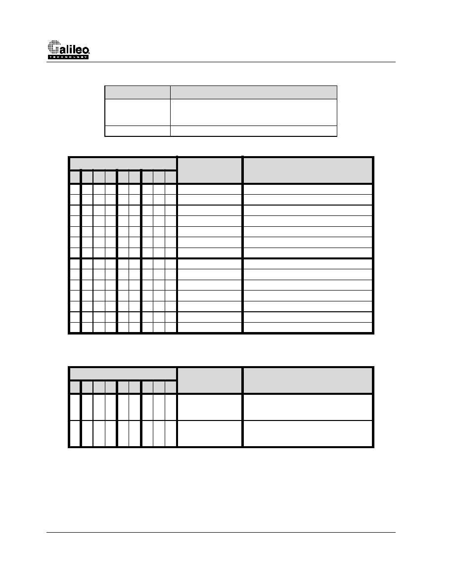
GT-64111 System Controller for RC4640, RM523X and VR4300 CPUs
16
Revision 1.0
1. `X' denotes "don't care" but `X' signals must be driven to a valid 0/1.
1. `X' denotes "don't care" but `X' signals are driven to a valid 0/1 by GT-64111.
SysCmd[4]
CPU mode select
0 - VR4300 mode
1 - R4600 mode
SysCmd[3:0]
Encoded to indicate size of the transfer
TABLE 2. Address Phase SysCmd[8:0] Encodings (driven by CPU/Local Master)
S y s C m d [ 8 : 0 ] E n c o d i n g
1
C o m m a n d
M n e m o n i c
C o m m a n d D e s c r i p t i o n
8
7
6
5
4
3
2
1
0
0
0
0
0
1
1
0
0
0
RdByte
Read a single byte
0
0
0
0
1
1
0
0
1
RdShort
Read 16 bits
0
0
0
0
1
1
0
1
0
RdTriByte
Read 3 bytes
0
0
0
0
1
1
0
1
1
RdWord
Read 4 bytes (single word)
0
0
0
0
1
1
1
X
X
Rd2Words
Read 2 words (8 bytes) in a burst
0
0
0
0
1
0
X
X
0
Rd4Words
Read 4 words (16 bytes) in a burst
0
0
0
0
1
0
X
X
1
Rd8Words
Read 8 words (32 bytes) in a burst
0
0
1
0
1
1
0
0
0
WrByte
Write a single byte
0
0
1
0
1
1
0
0
1
WrShort
Write 16 bits
0
0
1
0
1
1
0
1
0
WrTriByte
Write 3 bytes
0
0
1
0
1
1
0
1
1
WrWord
Write 4 bytes (single word)
0
0
1
0
1
1
1
X
X
Wr2Words
Write 2 words (8 bytes) in a burst
0
0
1
0
1
0
X
X
0
Wr4Words
Write 4 words (16 bytes) in a burst
0
0
1
0
1
0
X
X
1
Wr8Words
Write 8 words (32 bytes) in a burst
TABLE 3. Data Identifier SysCmd[8:0] Encodings (driven by GT-64111)
S y s C m d [ 8 : 0 ] E n c o d i n g
1
C o m m a n d
M n e m o n i c
C o m m a n d D e s c r i p t i o n
8
7
6
5
4
3
2
1
0
1
0
0
E
X
X
X
X
X
REOD
Indicates last valid data in a burst
E = 0 Data is good
E = 1 Data is erroneous
1
1
0
E
X
X
X
X
X
RD
Indicates valid data within a burst
E = 0 Data is good
E = 1 Data is erroneous
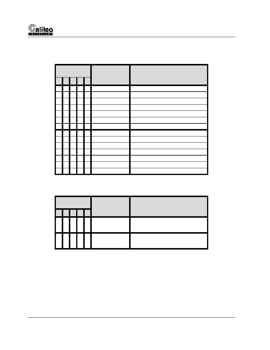
TABLE 1. SysCmd Bit Summary
S y s C m d B i t
F u n c t i o n

GT-64111 System Controller for RC4640, RM523X and VR4300 CPUs
Revision 1.0
3.2.1
SysAD Read Protocol
SysAD reads occur in three phases:
∑
The address phase in which address information is driven on the SysAD bus and command information is
driven on SysCmd.
∑
The mid-burst data phase during which the GT-64111 drives data on the SysAD bus and a data identifier on
SysCmd. The mid-burst data phase is entered between the address phase and the last data of the burst.
∑
The last data phase of the burst is when the GT-64111 drives data on the SysAD bus and a read end-of-data
(REOD) data identifier on SysCmd.
The address phase for all transactions begin with the assertion of ValidOut* to the GT-64111. Valid address and com-
mand information must be present on SysAD and SysCmd during this phase. Release* must also be asserted to the
GT-64111 to indicate that the CPU/Local Master is releasing mastership of the SysAD/SysCmd buses to the GT-64111
for completion of the read. ValidOut* is deasserted at the end of the address phase since the CPU/Local Master is no
longer driving information on SysAD/SysCmd.
For transactions longer than 32 bits, the mid-burst data phase is entered next. The GT-64111 will drive valid data on
SysAD, a valid data identifier (mnemonic = RD) on SysCmd, and will assert ValidIn* to qualify the SysAD and SysCmd
buses (see Figure 2).
The last data phase of the read burst is differentiated from the mid-burst state by the REOD data identifier driven on the
SysCmd bus. The last data phase of the burst is also entered for the datum returned for a single word, or sub-word,
read.
On the clock cycle following REOD, the GT-64111 floats the SysAD and SysCmd buses, returning ownership to the
CPU/Local Master.
Figure 2: Single Word Read Through CPU/Local Master Interface
1. `X' denotes "don't care" but `X' signals are driven to a valid 0/1.
TABLE 4. CPU/Local Master Data Identifier SysCmd[8:0] Encodings (driven by CPU/Local Master)
S y s C m d [ 8 : 0 ] E n c o d i n g
1
C o m m a n d
M n e m o n i c
C o m m a n d D e s c r i p t i o n
8
7
6
5
4
3
2
1
0
1
0
1
E
X
X
X
X
X
WEOD
Indicates last valid data in a burst
E = 0 Data is good
E = 1 Data is erroneous
1
1
1
E
X
X
X
X
X
WD
Indicates valid data within a burst
E = 0 Data is good
E = 1 Data is erroneous
ADDR
RDWORD
DATA
REOD
TClk
ValidOut*
SysAD[31:0]
SysCmd[8:0]
Release*
ValidIn*

GT-64111 System Controller for RC4640, RM523X and VR4300 CPUs
18
Revision 1.0
Figure 3: Four Word Burst Read through CPU/Local Master Interface
3.2.2
SysAD Write Protocol
CPU/Local Master writes occur in three phases:
∑
The address phase in which address information is driven on the SysAD bus and command information is
driven on SysCmd.
∑
The mid-burst write data phase during which the CPU/Local Master drives data on the SysAD bus and a write
data identifier (mnemonic = WD) on SysCmd. The mid-burst write data phase is entered between the address
phase and the last data phase of the write burst.
∑
The last data phase of the write burst is when the CPU/Local Master drives data on the SysAD bus and a write
end-of-data (WEOD) data identifier on SysCmd.
The address phase for write transactions begin with the assertion of ValidOut* to the GT-64111. Valid address and
command information must be present on SysAD and SysCmd during this phase. Release* remains high for write
transactions since the CPU/Local Master is not relinquishing ownership of the bus. ValidOut* is remains asserted
throughout a write transaction as the CPU/Local Master always driving valid information on SysAD/SysCmd.
For transactions longer than 32 bits, the mid-burst data write phase is entered next. The CPU/Local Master drives valid
data on SysAD, a valid write data identifier (mnemonic = WD) on SysCmd (see Figure 4).
Figure 4: CPU/Local Master Burst Write
ADDR
RD4WORDS
DATA 1
RD
DATA 2
DATA 3
DATA 4
RD
RD
REOD
WAIT STATE
TClk
ValidOut*
SysAD[31:0]
SysCmd[8:0]
Release*
ValidIn*
DATA SHOULD BE SAMPLED BY CPU/LOCAL MASTER HERE
MID-BURST DATA READ PHASE
ADDRESS PHASE
LAST DATA PHASE OF BURST
ADDR
WR4WORD
DATA 1
WD
DATA 2
DATA 3
DATA 4
WEOD
TClk
ValidOut*
WrRdy*
SysAD[31:0]
SysCmd[8:0]
Release*
ValidIn*
MID-BURST DATA WRITE PHASE
ADDRESS PHASE
LAST DATA PHASE OF THE BURST

GT-64111 System Controller for RC4640, RM523X and VR4300 CPUs
Revision 1.0
The last data phase of the write burst is differentiated by from the mid-burst state by the WEOD data identifier driven on
the SysCmd bus. The last data phase of the burst is also entered for the datum written for a single word, or sub-word,
write. On the clock cycle following WEOD, the GT-64111 returns to the idle state.
NOTE:
CPU/Local Master writes cannot be issued as long as WrRdy* is deasserted (HIGH). If WrRdy* is high and an
CPU/Local Master write is attempted, data from previous write cycles may be corrupted (see section 3.4.) Note that all
MIPS compliant processors follow this protocol, it is only DMA engines on the SysAD bus that need to be concerned
with sampling WrRdy* before initiating a write.
3.3
4300 Bus Mode Support (5-bit SysCmd Mode)
The GT-64111 can automatically detect (during the first read transaction) when a 4300 bus compatible processor is
attached. The 4300 uses a 5-bit SysCmd bus encoding that is similar, but incompatible, with the 9-bit SysCmd used by
4640 style processors. All other bus signals and timings are compatible between the two processor bus protocols.
The encodings for SysCmd[4:0] are shown in the tables below. Note that many encodings are not defined; these
encodings are reserved and must not be used. In 4300 mode, SysCmd[8:5] are not used and should be tied to GND. A
summary of bit usage is shown below.
TABLE 5. SysCmd Bit Summary
S y s C m d B i t
F u n c t i o n
SysCmd[4]
0 = Transaction information (read/write/size)
1 = Data information (good/bad/last)
SysCmd[3]
Read/Write Indicator for address cycles
0 = Read transaction
1 = Write transaction
Last data indicator for data cycles
0 = Last data
1 = Not last data
SysCmd[2]
Read/Write Attributesfor address cycles
0 = single read/write
1 = block read/write
Response data indicator for data cycles
0 = response data
1 = not response data
Reserved for CPU driven data cycles
SysCmd[1:0]
Size indicator for reads/writes for address cycles
Error status indicator for data cycles.
GT-64111 System Controller for RC4640, RM523X and VR4300 CPUs
20
Revision 1.0
1. `X' denotes "don't care" but `X' signals are driven to a valid 0/1.
TABLE 6. Address Phase SysCmd[4:0] Encodings (driven by CPU/Local Master)
S y s C m d [ 4 : 0 ]
E n c o d i n g
C o m m a n d
M n e m o n i c
C o m m a n d D e s c ri p t i o n
4
3
2
1
0
0
0
0
0
0
RdByte
Read a single byte
0
0
0
0
1
RdShort
Read 16 bits
0
0
0
1
0
RdTriByte
Read 3 bytes
0
0
0
1
1
RdWord
Read 4 bytes (single word)
0
0
1
0
0
Rd2Words
Read 2 words (8 bytes) in a burst
0
0
1
0
1
Rd4Words
Read 4 words (16 bytes) in a burst
0
0
1
1
0
Rd8Words
Read 8 words (32 bytes) in a burst
0
1
0
0
0
WrByte
Write a single byte
0
1
0
0
1
WrShort
Write 16 bits
0
1
0
1
0
WrTriByte
Write 3 bytes
0
1
0
1
1
WrWord
Write 4 bytes (single word)
0
1
1
0
0
Wr2Words
Write 2 words (8 bytes) in a burst
0
1
1
0
1
Wr4Words
Write 4 words (16 bytes) in a burst
0
1
1
1
0
Wr8Words
Write 8 words (32 bytes) in a burst
TABLE 7. Data Identifier SysCmd[4:0] Encodings (driven by GT-64111)
S y s C m d [ 4 : 0 ]
E n c o d i n g
1
C o m m a n d
M n e m o n i c
C o m m a n d D e s c ri p t i o n
4
3
2
1
0
1
0
0
E
X
REOD
Indicates last valid data in a burst
E = 0 Data is good
E = 1 Data is erroneous
1
1
0
E
X
RD
Indicates valid data within a burst
E = 0 Data is good
E = 1 Data is erroneous

GT-64111 System Controller for RC4640, RM523X and VR4300 CPUs
Revision 1.0
3.4
Operation of WrRdy* and the Internal Write Posting Queues
The GT-64111's CPU/Local Master interface includes a write posting queue that absorbs local CPU/Local Master
writes at zero wait-states. This is required per the MIPS SysAD bus write protocol.
The write posting queue has 4 address entries and 16 32-bit data entries. The GT-64111 signals if there is "room" in the
CPU/Local Master write posting queue by asserting WrRdy*. If WrRdy* is asserted then the CPU/Local Master may
issue a write of up to 8 words.
WrRdy* will be deasserted the cycle immediately following when:
∑
The address FIFO has two valid entries and a third address is being pushed, or...
∑
The address FIFO has more than two valid entries, or...
∑
The address FIFO has two valid entries or more, the data FIFO has four valid entries and a fifth one is being
pushed, or...
∑
The address FIFO has two valid entries or more, the data FIFO has more than four valid entries, or...
∑
The address FIFO has one valid entry, the data FIFO has six valid entries and a seventh one is being pushed,
or...
∑
The address FIFO has one valid entry, the data FIFO has more than six valid entries.
WrRdy* will be re-asserted the cycle following a transaction away from the states above.
It is not necessary to take the above scenarios into account when designing a system with the GT-64111. MIPS compli-
ant processors such as the R4640 and R4650 sample WrRdy* automatically before issuing a write. Only DMA devices
on SysAD need to be concerned about the functionality of WrRdy*, as mentioned above.
3.5
MIPS Write Modes and Write Patterns Supported
The GT-64111 supports both pipelined and R4000 compatible write modes (with 2 dead cycles between consecutive
writes). The default mode is pipelined, however R4000 mode can be selected in the CPU/Local Master Interface Con-
figuration Register.
The CPU/Local Master interface supports only DDDDDDDD and DXDXDXDXDXDXDXDX write patterns. Be sure to
select one of these two write patterns via the MIPS serial initialization bitstream during the CPU/Local Master reset pro-
cess.
3.6
CPU/Local Master Interface Endianess
The GT-64111 provides the capability to swap the endianess of data transferred to/from the internal registers, to/from
the PCI interface, and to/from the memory bus. Please see the relevant chapter in the applications section for more
information.
1. `X' denotes "don't care" but `X' signals are driven to a valid 0/1.
TABLE 8. CPU/Local Master Data Identifier SysCmd[4:0] Encodings (driven by CPU/Local
Master
S y s C m d [ 4 : 0 ]
E n c o d i n g
1
C o m m a n d
M n e m o n i c
C o m m a n d D e s c r i p t i o n
4
3
2
1
0
1
0
1
E
X
WEOD
Indicates last valid data in a burst
E = 0 Data is good
E = 1 Data is erroneous
1
1
1
E
X
WD
Indicates valid data within a burst
E = 0 Data is good
E = 1 Data is erroneous

GT-64111 System Controller for RC4640, RM523X and VR4300 CPUs
22
Revision 1.0
3.7
Burst Order
The GT-64111 supports the sub-block ordered bursts used by Orion MIPS processors, by default. Sub-block ordered
bursts are optimized for the burst patterns used by most synchronous SRAMs and SDRAMs.
Linear burst order is also supported for attaching processors other than the MIPS family. Linear burst order is enabled
by setting bit 9 in the DRAM Bank2 Parameters register at offset 0x454.
3.8
CPU/Local Master Interface Restrictions
1.
The CPU should not attempt an access before 10 TClk cycles following deassertion of Rst* have expired.
2.
CacheOpMap should not be written to a value other than 0 unless CachePres bit is set (see Register Section).
3.
The CPU Interface supports only DDDDDDDD and DXDXDXDXDXDXDXDX write patterns.
4.
A PCI I/O read intended for synchronization barrier should not be more than one long word (4 bytes). Any PCI I/O
read of more than 4 bytes will be carried out without checking the internal FIFOs.
5.
A write of more than 4 bytes to internal space will be ignored. A read of more than 4 bytes to internal space will
result in transaction termination with bus-error indication (SysCmd[5] equal `1').
6.
ValidOut* signal must have a pullup resistor to VCC. This is done in order to prevent GT-64111 to identify wrongly
the CPU type (RC4640/RM523X or R4300) due to unstable ValidOut* signal when getting out of reset.

GT-64111 System Controller for RC4640, RM523X and VR4300 CPUs
Revision 1.0
4.
Address Space Decoding
The GT-64111 has a fully programmable address map. Two address spaces exist: the CPU/Local Master address
space and the PCI address space (see Figure 5.) Both address maps use a two-stage decoding process where major
device regions are decoded first, then the individual devices are subdecoded.
Figure 5: Two Stage Address Decoding- Conceptual View
D R A M B a n k
R A S 0
-or-
R A S 1
D R A M B a n k
R A S 3
-or-
R A S 2
Galileo
Internal
Registers
Devices
(Multiple
Decoders)
Device Decoders
R A S 0
Bank
R A S 1
Bank
R A S 2
Bank
R A S 3
Bank
BootCS*
C S 0 *
C S 1 *
C S 2 *
C S 3 *
D R A M B a n k
R A S 0
-or-
R A S 1
D R A M B a n k
R A S 3
-or-
R A S 2
Galileo
Internal
Registers
PCI
M e m o r y 0
W i n d o w
PCI
I/O
W i n d o w
Devices
(Multiple
Decoders)
PCI
M e m o r y 1
W i n d o w
Internal Galileo Registers
To PCI Bus
Device Bus (AD
Bus)
Device Control
Signals
PCI Base
Address
Registers
Processor
D e c o d e
Registers

GT-64111 System Controller for RC4640, RM523X and VR4300 CPUs
24
Revision 1.0
4.1
Two Stage Decoding Process
The system resources are divided into eight groups: RAS[1:0], RAS[3:2], CS[2:0], CS[3] & BootCS, Internal Registers,
PCI I/O, and PCI Memory0/1. Each group can have a minimum of 2 Mbytes and a maximum of 256 Mbytes of address
space. The individual devices in the device groups (e.g. RAS[0]) are further sub decoded to 1 Mbyte resolution. Table 9
shows the CPU/Local Master decode and device sub-decode associations, Table 10 shows the same process for PCI.
1. This mapping also applies to the swap BARs located in PCI function 1, if enabled.
2. This feature is available only in the GT-64011-P-1 stepping
TABLE 9. CPU/Local Master and Device Decoder Mappings
CP U / L o c a l M a s t e r
D e c o d e r
As s o c i a t e d D e v i c e S u b - De c o d e r s
RAS[1:0]
Ras0*
Ras1*
RAS[3:2]
Ras2*
Ras3*
CS[2:0]
CS0*
CS1*
CS2*
BootCS*/CS3*
BootCS*
CS3*
PCI I/O
None, accesses decoded for PCI I/O are
bridged to PCI I/O transfers.
PCI Memory 0/1
None, accesses decoded for PCI Memory 0/1
are bridged to PCI Memory transfers.
Internal
None, decodes to GT-64111 internal registers.
TABLE 10. PCI Base Address Register and Device Decoder Mappings
P C I B a s e A d d r e s s
Re g i s t e r ( BA R)
D e c o d e r
1
As s o c i a t e d D e v i c e S u b - De c o d e r s
RAS[1:0]
- BAR 0 at 0x10
Ras0*
Ras1*
RAS[3:2]
- BAR 1 at 0x14
Ras2*
Ras3*
CS[2:0]
- BAR 2 at 0x18
Cs0*
Cs1*
Cs2*
BootCS*/Cs3*
- BAR 3 at 0x1C
BootCS*
Cs3*
Internal Registers (Memory)
- BAR 4 at 0x20
None, decodes PCI memory accesses to GT-
64111 internal registers.
Internal Registers (I/O)
- BAR 5 at 0x24
None, decodes PCI I/O accesses to GT-64111
internal registers.
Expansion ROM
- BAR at 0x30
None, decodes directly to CS3*
2

GT-64111 System Controller for RC4640, RM523X and VR4300 CPUs
Revision 1.0
4.1.1
CPU/Local Master Side Decoding Process
Decoding on the CPU/Local Master side starts with the SysAD address being compared with the values in the various
CPU/Local Master Low and High decoder registers. For example, the RAS[1:0] CPU/Local Master High and Low
decoder registers set the address range in which the Ras0* and Ras1* signals are active (i.e. where DRAM banks 0
and 1 are located.) The comparison works as follows:
∑
Bits 31:28 of the SysAD address are compared against bits 10:7 in the various CPU/Local Master Low decode
registers. These values much match exactly. This effectively sets a 256 Mbyte "page" for the resource group.
∑
Bits 27:21 of the SysAD address are then compared against bits 6:0 in the various CPU/Local Master Low
decode registers. The value of the SysAD bits must be greater than or equal to the Low decode value. This
sets the lower boundary for the region.
∑
Bits 27:21 of the SysAD address are then compared against the High decode registers. The value of the
SysAD bits must be less than or equal to this value. This sets the upper bound for the region.
∑
If all of the above are true, then the resource group is selected and a subdecode is perfomed to determine the
specific resource.
Once a CPU/Local Master resource group has been decoded, it must be subdecoded to determine which physical
device should be accessed within that group. This decoding is controlled by the device Low and High decode registers.
The comparison works as follows:
∑
Bits 27:20 of the SysAD address are then compared against the relevant device Low decode registers. The
value of the SysAD bits must be greater than or equal to the Low decode value. This sets the lower boundary
for the sub-decode region.
∑
Bits 27:20 of the SysAD address are then compared against the relevant device High decode registers. The
value of the SysAD bits must be less than or equal to this value. This sets the upper bound for the sub-decode
region.
∑
If all of the above are true, then the specific device is selected and an access to that device is performed.
Examples of the CPU/Local Master-side decode process are shown in Figure 6 and Figure 7.
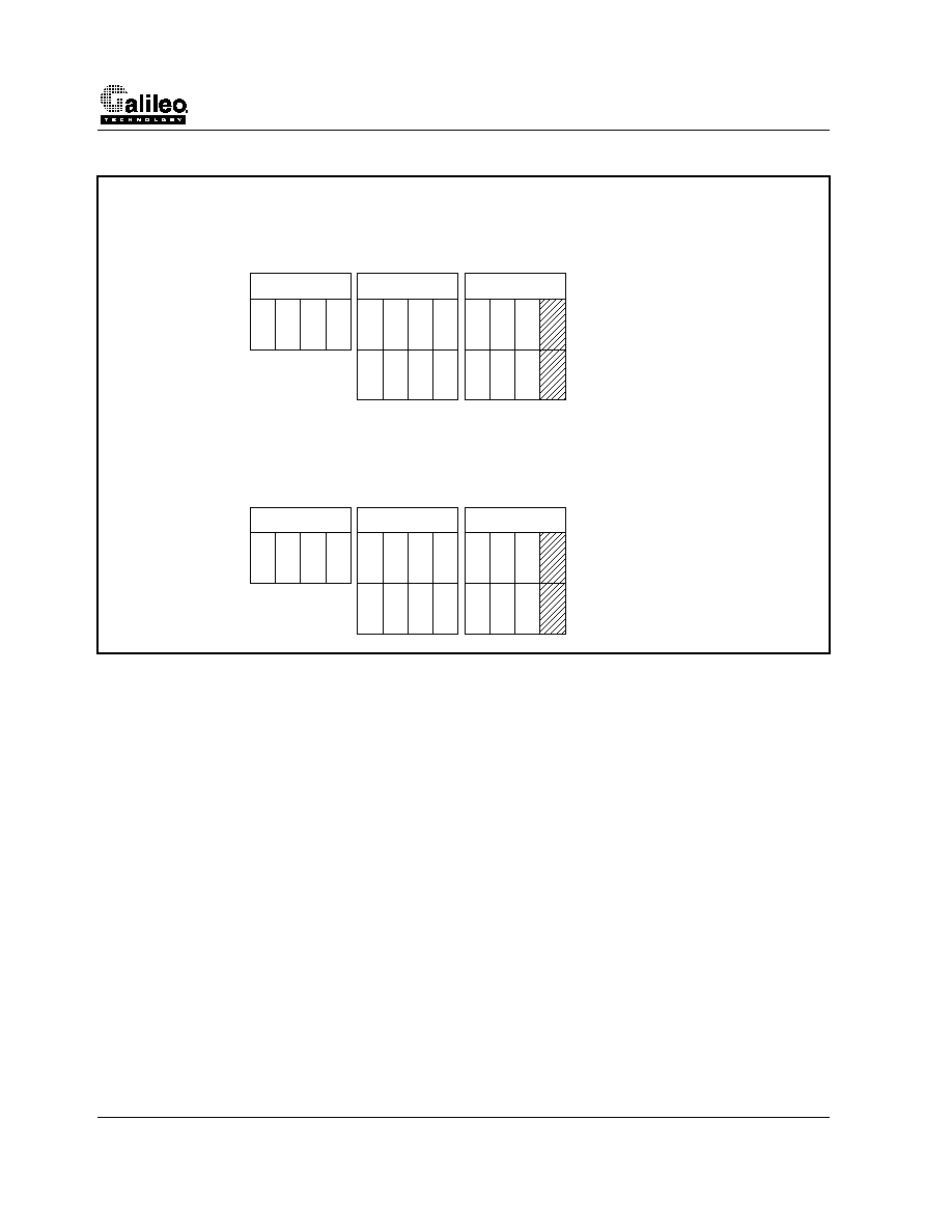
GT-64111 System Controller for RC4640, RM523X and VR4300 CPUs
26
Revision 1.0
Figure 6: CPU/Local Master-Side Resource Group Decode Function and Example
=
=
=
=
> =
> =
> =
> =
> =
> =
> =
31 30 29 28
27 26 25 24
23 22 21 20
< =
< =
< =
< =
< =
< =
< =
L o w P r o c e s s o r
D e c o d e R e g
H i g h P r o c e s s o r
D e c o d e R e g
S y s A D A d d r e s s
Bits
0
1
0
0
0
0
0
0
0
0
0
31 30 29 28
27 26 25 24
23 22 21 20
0
0
1
1
1
1
1
L o w P r o c e s s o r
D e c o d e R e g
H i g h P r o c e s s o r
D e c o d e R e g
S y s A D A d d r e s s
Bits
Example: Set up a SysAD decode region that starts at 0x4000.0000
and is 64Mbytes in length (0x4000.0000 to 0x43FF.FFFF):
If the SysAD address is between the Low and the High decode
addresses, then the access is passed to the Device Unit for sub-
decode.

GT-64111 System Controller for RC4640, RM523X and VR4300 CPUs
Revision 1.0
Figure 7: Device Sub-Decode Function and Example
=
=
=
=
> =
> =
> =
> =
> =
> =
> =
31 30 29 28
27 26 25 24
23 22 21 20
< =
< =
< =
< =
< =
< =
< =
L o w P r o c e s s o r
D e c o d e R e g
H i g h P r o c e s s o r
D e c o d e R e g
S y s A D A d d r e s s
Bits
< =
< =
< =
< =
< =
< =
< =
< =
> =
> =
> =
> =
> =
> =
> =
> =
A match ("hit") in the
processor decoders
forwards the address to the
device sub-decoders
L o w D e v i c e
D e c o d e R e g
H i g h D e v i c e
D e c o d e R e g
0
1
0
0
0
0
0
0
0
0
0
31 30 29 28
27 26 25 24
23 22 21 20
0
0
1
1
1
1
1
Low Processor
D e c o d e R e g
High Processor
D e c o d e R e g
SysAD Address
Bits
0
0
0
0
0
1
1
1
0
0
0
0
0
0
0
0
A match in the processor
decoders forwards the
address to the device sub-
decoders
Low Device
D e c o d e R e g
High Device
D e c o d e R e g
Processor Resource
Group Decode Region
(64Mbyte)
0x43FF.FFFF
Device Sub-Decode
Region
(8 Meg)
0x4000.0000
0x407F.FFFF
Example: Using the previous CPU/Local Master decode example (0x4000.0000 to
0x43FF.FFFF), place a device sub-decode in the first 8 Meg:
0x4000.0000 to 0x407F.FFFF

GT-64111 System Controller for RC4640, RM523X and VR4300 CPUs
28
Revision 1.0
4.2
PCI Side Decoding Process
Decoding on the PCI side starts with the PCI address being compared with the values in the various Base Address
Registers. For example, the RAS[1:0] Base Address Register sets the PCI base address range in which the Ras0* and
Ras1* signals are active (i.e. where DRAM banks 0 and 1 are located in PCI space.)
The size of the "window" in PCI space for each Base Address Register is set by the Bank Size registers for each Base
Address Register. The bank size sets which address bits are significant for the comparison between the active PCI
address and the values in the Base Address Registers (see Figure 8).
Figure 8: Bank Size Register Function Example (16Meg Decode)
The comparison works as follows:
∑
Bits 31:N of the PCI address are compared against bits 31:N in the various Base Address Registers (BAR).
These values much match exactly. The value of `N' is set by the least significant bit with a `0' in the Bank Size
Registers (for example, `N' would be equal to 24 in the example shown in Figure 8, above.)
∑
If all of the above is true, then the resource group is selected and a subdecode is perfomed to determine the
specific resource.
Once a resource group has been decoded by a BAR, it must be subdecoded to determine which physical device
should be accessed within that group. This decoding is controlled by the Device Low and High decode registers.
Note
that these registers are the same ones used for CPU/Local Master-side decoding. This means that the PCI and SysAD
memory maps are coupled at the device decoders. Address bits 27:20 (the bits compared by the Device decoders) for
any given device overlap in both the PCI and SysAD maps.
The sub-decoding comparison works as follows:
∑
Bits 27:20 of the PCI address are then compared against bits the relevant device Low decode registers. The
value of the PCI address bits must be greater than or equal to the Low decode value. This sets the lower
boundary for the sub-decode region.
∑
Bits 27:20 of the PCI address are then compared against the relevantbdevice High decode registers. The
value of the PCI address bits must be less than or equal to this value. This sets the upper bound for the sub-
decode region.
∑
If all of the above are true, then the specific device is selected and an access to that device is performed.
Note that the coupling of the SysAD, PCI, and device memory maps requires special attention for designers of PC Plug
and Play adapters. Please see Galileo's apnote for this application on our website.
4.3
Disabling the Device Decoders
Any Device sub-decoder can be disabled by setting the value of the "Low" decoder to be higher than the "High"
decoder.
4.4
DMA Unit Address Decoding
The DMA controller uses the address mapping of the CPU/Local Master interface when accessing the device/DRAM
bus. The DMA Unit can access the PCI bus independent of the CPU/Local Master-side PCI bridge decoders on the
GT-64011 and GT-64060 devices only (see DMA section.)
0
0
0
0
0
0
0
0
1
1
1
31 30 29 28
27 26 25 24
23 22 21 20
1
B a n k S i z e R e g
P C I A d d r e s s
Bits
1
1
1
1
1
1
1
19 18 17 16
15 14 13 12
1
=
=
=
=
=
=
=
=
x
x
x
x
x
x
x
x
x
x
x
x
'=' means must match exactly
'x' means don't care
C o m p a r i s o n
against PCI
a d d r e s s

GT-64111 System Controller for RC4640, RM523X and VR4300 CPUs
Revision 1.0
4.5
Address Space Decoding Errors
When the CPU/Local Master tries to access an address from the SysAD that is not supported, the GT-64111 will latch
the address into the Bus Error register, and will issue a bus error (over SysCmd[5]) if the access was a read access,
and an interrupt if it was a read or write access. This feature is especially useful during software debug, when errant
code can cause fetches from unsupported addresses.
When a PCI access hits in a Base Address Register then
misses in the associated subdecoders, the result will be ran-
dom data returned on a read; write data is discarded. The MemOut bit in the interrupt Cause register is also set.
Accesses that miss all of the GT-64111 BARs result in no response at all from the GT-64111, as you would expect.
NOTE: Address space decoders must never be programmed to overlap; unpredictable behavior will result.
4.6
Default Memory Map
The default CPU/Local Master memory map that is valid following RESET is shown in Table 11 below. The default PCI
map and BAR sizing information is shown in Table 12 and Table 13.
TABLE 11. CPU/Local Master and Device Decoder Default Address Mapping
C P U/ L o c a l M a s t e r D e c o d e
R a n g e a n d S i z e
R e s o u rc e
Gr o u p
D e v i c e D e c o d e
R a n g e a n d S i z e
De v i c e
S e l e c t e d
0x0 to 0x00FF.FFFF
16 Megabytes
RAS[1:0]
0x0 to 0x007F.FFFF
8 Megabytes
Ras0*
0x0080.0000 to 0x00FF.FFFF
8 Megabytes
Ras1*
0x0100.0000 to 0x01FF.FFFF
16 Megabytes
RAS[3:2]
0x0100.0000 to 0x017F.FFFF
8 Megabytes
Ras2*
0x0180.0000 to 0x01FF.FFFF
8 Megabytes
Ras3*
0x1000.0000 to 0x11FF.FFFF
32 Megabytes
PCI I/0
No subdecode, access bridged
directly to PCI I/O space
PCI
0x1200.0000 to 0x13FF.FFFF
32 Megabytes
PCI Mem0
No subdecode, access bridged
directly to PCI memory space
PCI
0x1C00.0000 to 0x1E1F.FFFF
~32 Megabytes
CS[2:0]
0x1C00.0000 to 0x1C7F.FFFF
8 Megabytes
CS0*
0x1C80.0000 to 0x1CFF.FFFF
8 Megabytes
CS1*
0x1D00.0000 to 0x1DFF.FFFF
16 Megabytes
CS2*
0x1F00.0000 to 0x1FFF.FFFF
16 Megabytes
CS[3] and
BootCS*
0x1F00.0000 to 0x1FBF.FFFF
12 Megabyte
CS3*
0x1FC0.0000 to 0x1FFF.FFFF
4 Megabytes
BootCS*
0xF200.0000 to 0xF3FF.FFFF
32 Megabytes
PCI Mem1
No subdecode, access bridged
directly to PCI memory space
PCI

GT-64111 System Controller for RC4640, RM523X and VR4300 CPUs
30
Revision 1.0
TABLE 12. PCI Function 0 and Device Decoder Default Address Mapping
P CI F u n c t i o n 0 D e c o d e
R a n g e a n d S i z e
R e s o u rc e
Gr o u p
D e v i c e D e c o d e
R a n g e a n d S i z e
De v i c e
S e l e c t e d
0x0 to 0x00FF.FFFF
16 Megabytes in Memory Space
RAS[1:0]
0x0 to 0x007F.FFFF
8 Megabytes
Ras0*
0x0080.0000 to 0x00FF.FFFF
8 Megabytes
Ras1*
0x0100.0000 to 0x01FF.FFFF
16 Megabytes in Memory Space
RAS[3:2]
0x0100.0000 to 0x017F.FFFF
8 Megabytes
Ras2*
0x0180.0000 to 0x01FF.FFFF
8 Megabytes
Ras3*
0x1400.0000 to 0x1400.0FFF
4 Kbytes in Memory Space
Internal
Registers
No subdecode
Internal Registers
0x1400.0000 to 0x1400.0FFF
4 Kbytes in I/O Space
Internal
Registers
No subdecode
Internal Registers
0x1C00.0000 to 0x1DFF.FFFF
32 Megabytes in Memory Space
CS[2:0]
0x1C00.0000 to 0x1C7F.FFFF
8 Megabytes
CS0*
0x1C80.0000 to 0x1CFF.FFFF
8 Megabytes
CS1*
0x1D00.0000 to 0x1DFF.FFFF
16 Megabytes
CS2*
0x1F00.0000 to 0x1FFF.FFFF
16 Megabytes in Memory Space
CS[3] and
BootCS*
0x1F00.0000 to 0x1FBF.FFFF
12 Megabyte
CS3*
0x1FC0.0000 to 0x1FFF.FFFF
4 Megabytes
BootCS*
0x1F00.000 to 0x1FFF.FFFF
16 Megabytes (uses CS[3] and
BootCS* size register)
PCI
Expansion
ROM
No subdecode. This decoder is
used only during PC BIOS initial-
ization.
CS3*
TABLE 13. PCI Function 1 (Byte Order Swap) and Device Decoder Default Address Mapping
P CI F u n c t i o n 0 D e c o d e
R a n g e a n d S i z e
R e s o u rc e
Gr o u p
D e v i c e D e c o d e
R a n g e a n d S i z e
De v i c e
S e l e c t e d
0x0 to 0x00FF.FFFF
16 Megabytes in Memory Space
RAS[1:0]
0x0 to 0x007F.FFFF
8 Megabytes
Ras0*
0x0080.0000 to 0x00FF.FFFF
8 Megabytes
Ras1*
0x0100.0000 to 0x01FF.FFFF
16 Megabytes in Memory Space
RAS[3:2]
0x0100.0000 to 0x017F.FFFF
8 Megabytes
Ras2*
0x0180.0000 to 0x01FF.FFFF
8 Megabytes
Ras3*
0x1F00.0000 to 0x1FFF.FFFF
16 Megabytes in Memory Space
CS[3] and
BootCS*
0x1F00.0000 to 0x1FBF.FFFF
12 Megabyte
CS3*
0x1FC0.0000 to 0x1FFF.FFFF
4 Megabytes
BootCS*

GT-64111 System Controller for RC4640, RM523X and VR4300 CPUs
Revision 1.0
5.
Memory Controller
The GT-64111's Memory Controller consists of a DRAM Controller and a device Controller. The DRAM Controller has
an independent 12-bit address bus (DAdr[11:0]) and shares the 32-bit address/data (AD) bus for data transfers. The
device controller uses the 32-bit AD bus for both address and data transfers. All memory and I/O devices in a GT-
64111 system are connected to the AD bus (the SysAD bus is used primarily as a point-to-point connection between
CPU and chipset.) The memory controller will only master read and write transactions to DRAM or devices, as
instructed from the CPU, DMA controller, or a PCI master on the PCI bus.
A device on the AD bus may NOT master
transactions to other devices, DRAM or the PCI via the GT-64111's memory controller. The GT-64111's Memory Con-
troller can support 32 or 64-bit (32-bit interleaved) DRAM as well as 8-, 16-, 32-, and 64-bit (32-bit interleaved)
devices.
The GT-64111 implements a round robin arbitration scheme for requests of the memory controller as shown in Figure
9.
Figure 9: Memory Controller Arbitration
5.1
DRAM Controller
The DRAM controller supports up to four banks of page mode or EDO DRAM. The DRAM configuration register
(0x448) contains configuration information which is valid for all banks. Various access parameters can be programmed
on a per bank basis as each bank has its own parameters register (0x44c - 0x458). The supported address depth of
the DRAM can vary for each bank separately from 256K (9-bit RAS*, 9-bit CAS*) to 16M (12-bit RAS*, 12-bit CAS*),
and the width of each bank may be 32 bits or 64 bits (32-bit interleaved). With these options, each DRAM bank can
vary in size from 1 Mbyte to 128 Mbytes. The maximum total DRAM address space is 512Mbytes for four banks.
5.1.1
DRAM Refresh
5.1.1.1
Refresh Rates
The GT-64111 implements standard CAS* before RAS* refreshing. Refresh rates for all banks can be programmed to
occur at different frequencies according to the RefIntCnt, a 14-bit value DRAM configuration register. For example, the
default value of RefIntCnt is 0x200. If TClk is 50 MHz, than a refresh sequence will occur every 10us. This is derived
from 50MHz (=20ns) * 0x200 (512d) = 10.24us. Every instance that the refresh counter in the GT-64111 reaches its ter-
minal count, a refresh request is sent to the Memory Controller. This DRAM refresh request enters the arbiter, and the
refresh cycle will begin once the Memory Controller has been arbitrated for this request.
5.1.1.2
Non-staggered and staggered Refresh
Non-staggered or staggered refresh for all banks can be programmed according to StagRef in the DRAM configuration
register. In non-staggered refresh, RAS[3:0] will simultanously assert following the low-going CAS* refreshing all banks
at the same time as shown in Figure 10. If the DRAM Controller is programmed to performed staggered refresh
C P U
P C I
D M A
Controller
D R A M
Refresh

GT-64111 System Controller for RC4640, RM523X and VR4300 CPUs
32
Revision 1.0
(default), RAS[3:0] will not simulataneously assert LOW following the low-going CAS*. Rather, RAS[0] will first go LOW,
followed by RAS[1] on the next TClk, and so on. After the last RAS, RAS[3] has asserted LOW, CAS* will go HIGH
again followed by RAS[0] on the next TClk, RAS[1] on the following TClk, and so on. Staggered Refresh is useful for
load balancing, shown in Figure 11.
Figure 10: Non-Staggered Refresh Waveform
Figure 11: Staggered Refresh Waveform
5.1.2
Assymetrically RAS*/CAS* Addressing
The GT-64111 supports assymetrical RAS*/CAS* addressing. In other words, a different number of addressing bits
may be valid for row addressing as compared to column addressing. 9, 10, 11 or 12 bits can be used for DRAM row
addressing and is specified on a per bank basis by programming bits 5:4 of the DRAM Bank[3:0] Parameter registers
(0x44c-0x458). These bits determine the decoding of an address asserted on the SysAD bus from a device such as a
CPU or from a PCI System on the PCI bus. Some bits of the address are used for RAS* while others are used for
CAS*. The active SysAD or PAD pins which are translated to the DAdr pins are shown in Table 14 for 32-bit DRAM and
in Table 15 for 64-bit DRAM (32-bit interleaved).
TABLE 14. Active DAdr[11:0] bits for RAS* and CAS*, 32-bit DRAM
TABLE 15. Active DAdr[11:0] bits for RAS* and CAS*, 64-bit DRAM (32-bit interleaved)
1. Regardless of 5:4, DAdr[11:0] will always have the value of SysAD/PAD[16:5] during RAS*.
1. Regardless of 5:4, DAdr[11:0] will always have the value of SysAD/PAD[16:5] during RAS*.
DRAM Bank
Para. 5:4
Row Addr.
Depth
Active RAS*
DAdr Bits
1
SysAD/PAD Bits Used
for RAS* on DAdr
SysAD/PAD Bits Used for CAS* on
DAdr[11:0]
00
512
8:0
13:5
22..20, 16..14, 19..17, 4..2
01
1K
9:0
14:5
23..21, 16..15, 20..17, 4..2
10
2K
10:0
15:5
24..22, 16, 21..17, 4..2
11
4K
11:0
16:5
25..17, 4..2
DRAM Bank
Para. 5:4
Row Addr.
Depth
Active RAS*
DAdr Bits
1
SysAD/PAD Bits Used
for RAS* on DAdr
SysAD/PAD Bits Used for CAS* on
DAdr[11:0]
00
512
8:0
13:5
23..20, 16..14, 19..17, 4..3
01
1K
9:0
14:5
24..21, 16..15, 20..17, 4..3
10
2K
10:0
15:5
25..22, 16, 21..17, 4..3
11
4K
11:0
16:5
26..17, 4..3
TClk
RAS[3:0]
ECAS[3:0]
OCAS[3:0]
0
F
F
F
0
F
TClk
RAS[3:0]
ECAS[3:0]
OCAS[3:0]
8
C
E
F
7
3
1
0
F
F
F
0
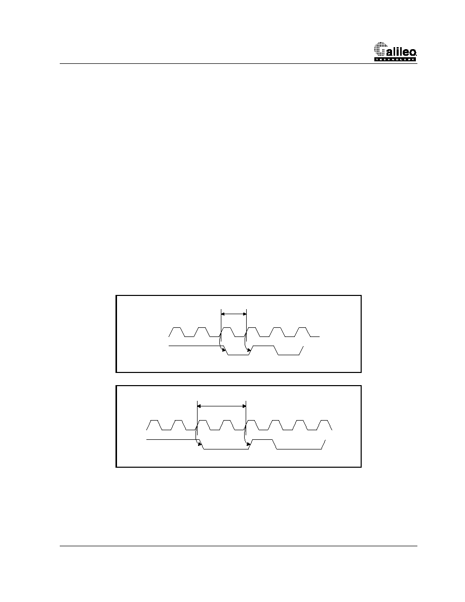
GT-64111 System Controller for RC4640, RM523X and VR4300 CPUs
Revision 1.0
For example, when using 32-bit DRAM, if bits 5:4 are 01, for a particular bank, an address decoded to that bank from
the SysAD/PAD bus will cause the DAdr bus to act as follows: During RAS* phase, DAdr[9:0] will have the values of
SysAD/PAD[13:5]. During CAS* phase, DAdr[11:0] will have the values of {SysAD/PAD[23:21], SysAD/PAD[16:15],
SysAD/PAD[20:17], SysAD/PAD[4:2]}.
5.1.3
DAdr[11]/ADS* Function
The default state of DAdr[11]/ADS* is to function only as DAdr[11]. Optionally, this pin is software configurable to only
behave as ADS* via bit 17 of the DRAM Configuration register. When this pin functions as ADS*, it is an active LOW
address strobe which indicates the beginning of a device transaction. This pin is sampled as an input at reset for con-
figuration purposes.
5.1.4
Programmable DRAM Timing Parameters
The DRAM controller of the GT-64111 supports a wide range of DRAMs with different access times and each bank can
be programmed independently by the DRAM Bank[3:0] Parameter registers (0x44c-0x458). These paramaters include
the number of clock cycles (based on TClk) that CAS* is asserted (LOW) in a write access (CASWr, bit 0) and in a read
access (CASRd, bit 2). The number of clocks cycles (based on TClk) between active RAS* and CAS* in a write access
(RAStoCASWr, bit 1) and in read access (RAStoCASRd, bit 3) can also be programmed.
5.1.4.1
Asserted CAS*
The number of clocks that CAS* is asserted in LOW in write and read accesses can be programmed to be either one
(Figure 12) or two clocks (Figure 13). 2 clocks is the default number that CAS* is LOW for both write and read
accesses. Both the high and low-going edges of CAS* are driven from a rising TClk.
Figure 12: CAS* Asserted for 1 Clock
Figure 13: CAS* Asserted for 2 Clocks
Selecting the CASWr and CASRd parameter will depend on
∑
DRAM CAS* pulse width minimum requirement time
∑
TClk frequency
For example, standard 60ns EDO DRAM has a 10ns minimum pulse requirement for CAS*. If TClk is set to 50 MHz
(20ns), both CASWr and CASRd can be programmed to one cycle for maximum performance. This will result in read-
ing/writing one datum every two clocks (for 32-bit DRAM). On the other hand, slower Page Mode DRAMs will have
CAS* LOW for 1 TClk
CAS* asserted
from Rising TClk
TClk
. . .
CAS* de-asserted
from Rising TClk
CAS*
CAS* LOW for 2 TClks
CAS* asserted
from Rising TClk
TClk
CAS* de-asserted
from Rising TClk
CAS*
. . .

GT-64111 System Controller for RC4640, RM523X and VR4300 CPUs
34
Revision 1.0
longer access times requiring the GT-64111 to assert CAS* for two clocks instead of one.
5.1.4.2
RAS* to CAS*
The number of clocks between active RAS* and CAS* in write and read accesses can be programmed to be either two
(Figure 14) or three clocks (Figure 15). 3 clocks is the default delay between active RAS* and active CAS*.
Figure 14: Two Clock Delay between Active RAS* to Active CAS*
Figure 15: Three Clock Delay between Active RAS* to Active CAS*
Selecting the RAStoCASWr and RAStoCASRd parameter will depend on
∑
DRAM RAS* to CAS* maximum delay time
∑
TClk frequency
5.1.5
DRAM Bank Width and Location
Bit 6 of the DRAM Bank[3:0] Parameter registers (0x44c-0x458), BankWidth, specifies whether the data width of the
particular bank of DRAM is 32-bit (default) or 64-bit (32-bit interleaved). If the bank is set for 32-bit operation, it can
either reside on the even (default) or odd bank by setting bit 7, BankLoc. Selecting the even or the odd bank allows for
load balancing.
If the BankWidth is programmed to `1' indicating the bank is set for 64-bit (32-bit interleaved), the setting of BankLoc is
irrelavent as both banks will be populated.
5.1.6
DRAM Performance
DRAM performance is based on the width of DRAM implemented (32 or 64-bit) as well as the setting of the DRAM
parameters. Table 16 lists the performance when the CPU reads a cache line (8 32-bit words) from DRAM. The perfor-
mance is measured from ValidOut* asserted by the processor with the Rd8Words command to the GT-64111 asserting
ValidIn* responding with the first datum. For example, 8-1-1-1-1-1-1-1 performances indicates 8 TClks from ValidOut*
asserted to ValidIn* asserted for the first datum and 1 TClk for every following datum (0 wait states). 10-3-3-3-3-3-3-3
indicates 10 TClks from ValidOut* asserted to ValidIn* asserted for the first datum and 3 TClks for every following
TClk
RAS*
. . .
CAS*
. . .
RAS* to CAS*,
2 TClks
TClk
RAS*
. . .
CAS*
. . .
RAS* to CAS*,
3 TClks

GT-64111 System Controller for RC4640, RM523X and VR4300 CPUs
Revision 1.0
datum (2 wait states).
TABLE 16. DRAM Performance
5.2
Device Controller
The device controller supports up to five banks of devices. Various access parameters can be programmed on a per
bank basis as each bank has its own parameters register (0x45c - 0x46c). The supported memory space of each
device bank can vary for each bank separately up to 32 Mbytes, and the width of each bank may be 8, 16, 32 or 64 bits
The maximum total device address space is 160Mbytes for five banks. The 5 individual chip selects are typically bro-
ken up into 4 individual device banks plus one chip select for a boot device (non-volatile memory).
BootCS* has the exact same functionality as CS[3:0] and devices which need to be read from and written to can be
attached to this chip select. The only difference between BootCS* and CS[3:0] is that by default, BootCS* is mapped to
the physical boot address of 0x1FC0.0000 (which can be reprogrammed) and its device width can be programmed by
input pins on reset.
Each device bank can have unique programmable timing parameters to accommodate different device types (e.g.
Flash, SRAM, ROM, I/O Controllers). The devices share the local AD bus with the DRAM, but unlike DRAM, the
devices use the AD bus as a multiplexed address and data bus.
In the address phase, the device controller puts on the AD bus an address with a corresponding Chip Select asserted.
ALE (and ADS* if programmed, Section 5.1.3) indicates the AD bus is outputing an address and CS*, DevRW* and
DMAAck*. ALE is used to latch the address, CS*, DevRW* and DMAAck* in an external 373. CS* should then be qual-
ified (OR-tied) with CSTiming*. A read or write cycle is indicated by the latched DevRW*. The CSTiming* signal will be
valid for the programmable number of cycles of the specific CS* that is active. TurnOff, AccToFirst and AccToNext can
be set in registers 0x45c - 0x46c for each bank's read timing parameters (see Figure 16 for waveform example without
latches enabled, see Figure 17 for waveform example with latches enabled). ADStoWr, WrActive and WrHigh can be
set for each bank's write timing parameters (see Figure 18 for waveform example). Please see Section 5.6 before con-
figuring these bits. AcctoFirst, AccToNext and WrActive can be extended by the Ready* pin (see Section 5.2.10).
5.2.1
TurnOff, bits [2:0]
TurnOff is the number of TClk cycles that the GT-64111 will not drive the memory bus after a read from a device. This
prevents contentions on the memory bus after a read cycle for a slow device. This parameter is measured from the the
number of cycles between the deassertion of DevOE* (an externally extracted signal which is the logical OR between
CSTiming* and inverted DevRW*) to an new AD bus cycle.
5.2.2
AccToFirst, bits [6:3]
AccToFirst defines the number of cycles in a read access from the assertion of CS* to the cycle that the data will be
latched (by external latches). This parameter can also be thought as the delay between the rising edge of TClk which
drives ALE HIGH to the the rising edge of TClk where the first data will be latched by the external latches. If there are
no latches in the system, AccToFirst defines the number of cycles between TClk which drives ALE HIGH to the rising
edge of TClk where the first data is latched into the GT-64111. This parameter can be extended by the Ready* pin.
5.2.3
AccToNext, bits [10:7]
AccToNext defined as the number of cycles in a read access from the cycle that the first data was latched to the cycle
1. 8-2-2-2-2-2-2-2 with 32-bit DRAMs and 8-1-1-1-1-1-1-1 clocks with 64-bit (32-bit interleaved) DRAMs is the performance for Ras-
toCasRd = 0 and CasRd = 0. In "wait-state" nomenclature this equates to 5-1-1-1-1-1-1-1 and 5-0-0-0-0-0-0-0.)
DRAM Width
RASt o C a s R d = 0
C A S R d = 0
1
RASt o C a s R d = 0
C AS Rd = 1
RASt o C a s Rd = 1
C A S R d = 0
RASt o C a s R d = 1
C AS R d = 1
32-bit
8-2-2-2-2-2-2-2
9-3-3-3-3-3-3-3
9-2-2-2-2-2-2-2
10-3-3-3-3-3-3-3
64-bit (32-bit
interleaved)
8-1-1-1-1-1-1-1
9-1-2-1-2-1-2-1
9-1-1-1-1-1-1-1
10-1-2-1-2-1-2-1

GT-64111 System Controller for RC4640, RM523X and VR4300 CPUs
36
Revision 1.0
to the next data will be latched (in burst accesses). This parameter can also be thought of as the delay between the ris-
ing edge of TClk which data is latched to the rising edge of TClk where the next data is latched in a burst cycle. This
parameter can be extended by the Ready* pin.
5.2.4
ADStoWr, bits[13:11]
There are eight byte write signals, four for even bank devices (EWr[3:0]*) and four for odd bank devices (OWr[3:0]*).
ADStoWr can also be thought as the delay between the rising edge of TClk which drives ADS* LOW (ALE HIGH) from
to the assertion of EWr* or OWr*, or for the first write pulse.
5.2.5
WrActive, bits[16:14]
WrActive is the number of TClks that EWr* and OWr* are active (asserted). This parameter is measured from the first
rising edge of TClk where EWr* or OWr* is asserted LOW to the last rising edge of TClk where EWr* or OWr* is LOW
for that particular write pulse. This parameter can be extended by the Ready* pin.
5.2.6
WrHigh, bits[19:17]
WrHigh is the number of TClks that EWr* and OWr* are inactive between burst writes. This parameter is measured
from the first rising edge of TClk where EWr* or OWr* is de-asserted HIGH to the last rising edge of TClk where EWr*
or OWr* is HIGH. On the next rising edge of TClk, EWr* and OWr* will be asserted LOW for the next write pulse.
These signals are driven off of the falling edge of TClk.
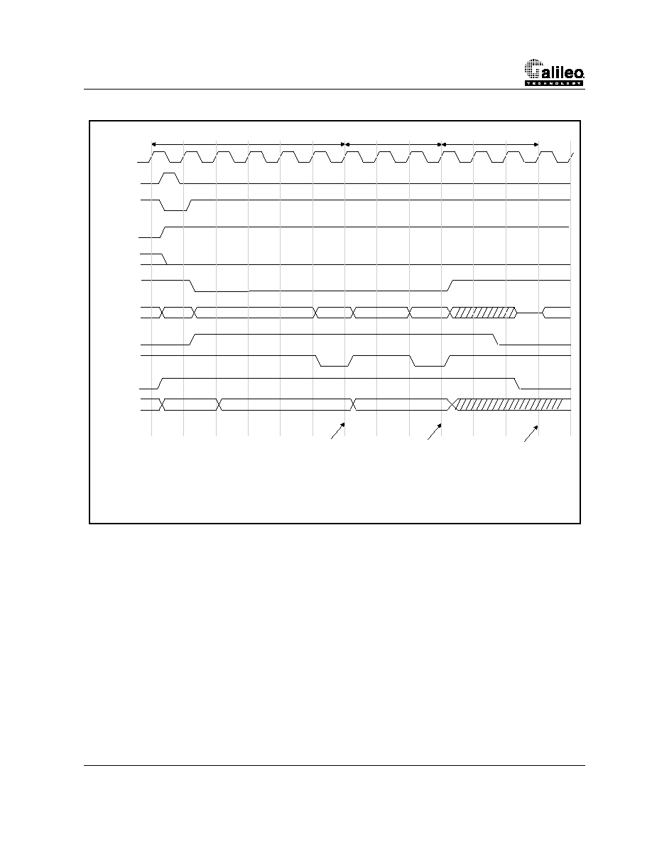
GT-64111 System Controller for RC4640, RM523X and VR4300 CPUs
Revision 1.0
Figure 16: Waveform Showing Device Read Parameters, LatchFunct = 0
A D D R E S S
TClk
A L E
A D S *
1
AD[31:0]
AcctoFirst = 6
AcctoNext = 3
TurnOff = 3
D A T A 1
CS*
2
CSTiming*
D e v R W *
Notes:
1. Assumes DAdr11/ADS* is programmed to be ADS* only
2. CS* is driven off the same rising TClk* as ALE (and ADS*). Throughout consecutive transactions to the same device, CS* will
remain asserted. This is why CS* must ALWAYS be qualified with CSTiming*.
3. AD[31:0] (DATA 1) sampled by GT-64011.
4. AD[31:0] (DATA 2) sampled by GT-64011.
5. GT-64011 may drive AD[31:0] after TurnOff.
6. OEB is programmed active LOW.
D A T A 2
3
4
5
O E B
LEE/
L E O
OEE*/
O E O *
Dev[31:0]
D A T A 1 D R I V E N F R O M D E V I C E
D A T A 2 D R I V E N F R O M D E V I C E
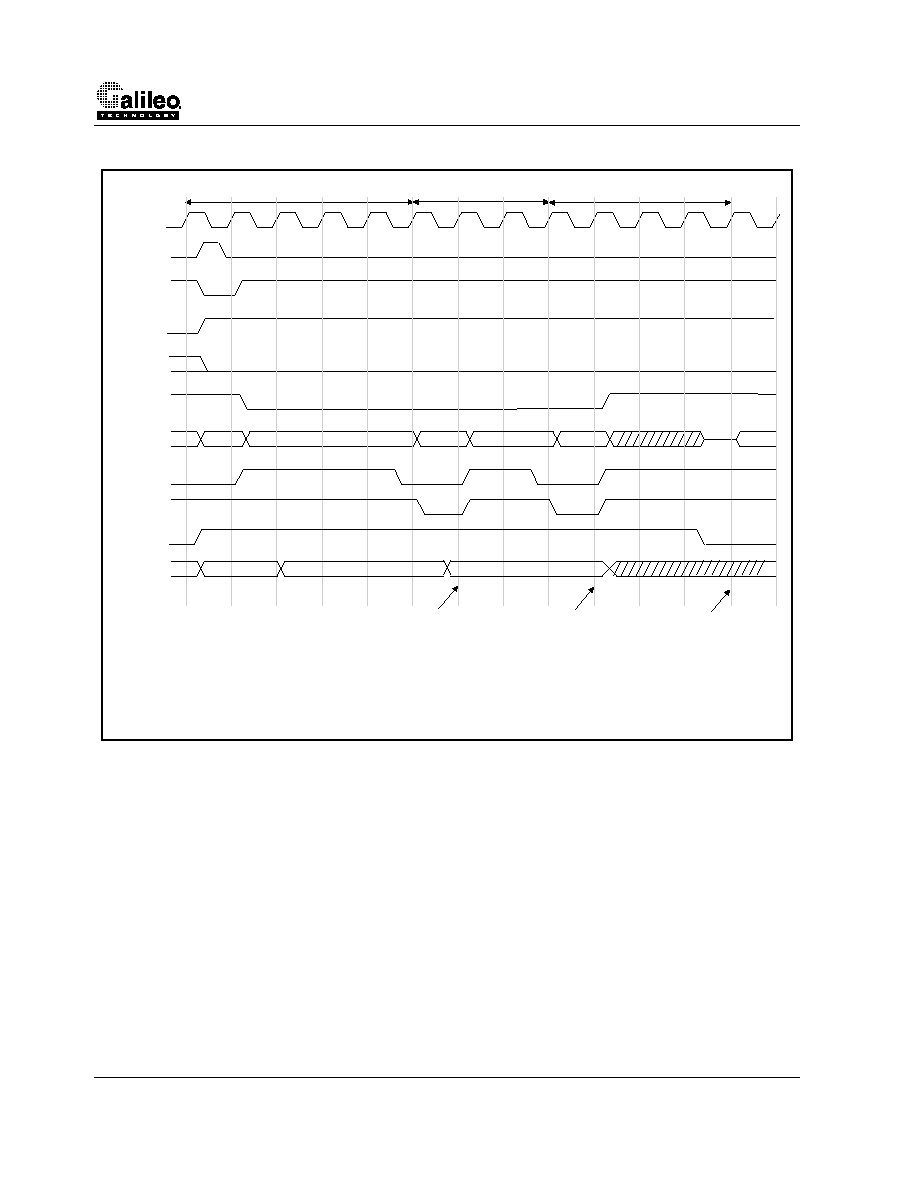
GT-64111 System Controller for RC4640, RM523X and VR4300 CPUs
38
Revision 1.0
Figure 17: Waveform Showing Device Read Parameters, LatchFunct = 1
A D D R E S S
TClk
A L E
A D S *
1
AD[31:0]
AcctoFirst = 5
AcctoNext = 3
TurnOff = 4
D A T A 1
CS*
2
CSTiming*
D e v R W *
Notes:
1. Assumes DAdr11/ADS* is programmed to be ADS* only
2. CS* is driven off the same rising TClk* as ALE (and ADS*). Throughout consecutive transactions to the same device, CS* will
remain asserted. This is why CS* must ALWAYS be qualified with CSTiming*.
3. AD[31:0] (DATA 1) sampled by GT-64011.
4. AD[31:0] (DATA 2) sampled by GT-64011.
5. GT-64011 may drive AD[31:0] after TurnOff.
6. OEB is programmed active LOW.
D A T A 2
LEE/
L E O
3
4
5
Dev[31:0]
D A T A 1 D R I V E N F R O M D E V I C E
D A T A 2 D R I V E N F R O M D E V I C E
OEE*/
O E O *
O E B

GT-64111 System Controller for RC4640, RM523X and VR4300 CPUs
Revision 1.0
Figure 18: Waveform Showing Device Write Parameters
5.2.7
Burst Transactions
The device controller supports a maximum of 8 32-bit word burst accesses. The burst address is supported by a three
bit wide address bus (BAdr[2:0]) that is different from the latched address on the multiplexed AD bus. Note that
BAdr[2:0] are the same pins as the least significant DRAM address lines, DAdr[2:0]. See pin assignment table for more
detail.
5.2.8
Packing and Unpacking Data and Burst Support
The GT-64111 supports the packing of data into a 32-bit word, in reads from devices that are 8 or 16-bits wide. Devices
that are 8-bits or 16-bits wide only are supported by partial reads (up to 64-bits). The controller supports CPU writes of
1 to 8 bytes to 8-bit or 16-bit wide devices. Therefore, 8 and 16-bit devices MUST NOT be mapped to cacheable
regions. The reason is that the R4640 has an 8-word (32 bytes) cache line size. This would equate to a burst of 32 8-
bit accesses or 16 16-bit accesses.
The GT-64111 supports cached accesses to 32 and 64-bit device spaces. It supports DMA/PCI writes of 1 to 4 bytes to
8-bit or 16-bit wide devices.
5.2.9
"Destructive" Reads
When the CPU performs an device read from an 8-bit device, there are certain conditions where the device controller
will fetch additional data even though it is never read by the CPU. Designers using devices such as FIFOs must be
aware of these "destructive" reads.
Destructive reads will not occur on read accesses from 16, 32 or 64-bit devices.
When a PCI master reads data from 8 or 16-bit devices, or when data is read from 8 or 16-bit devices via the DMA con-
A D D R E S S
TClk
A L E
A D S *
1
AD[31:0]
ADStoWr = 3
WrActive = 3
WrHigh= 3
WrActive = 3
E W r
O W r
3
G T - 6 4 0 1 1 D R I V E S V A L I D D A T A 1
G T - 6 4 0 1 1 D R I V E S V A L I D D A T A 2
C S *
2
CSTiming*
D e v R W *
Notes:
1. Assumes DAdr11/ADS* is programmed to be ADS* only.
2. CS* is driven off the same rising TClk* as ALE (and ADS*). Throughout consecutive transactions to the same device, CS* will
remain asserted. This is why CS* must ALWAYS be qualified with CSTiming*.
3. EWr[3:0]* and OWr[3:0]* are asserted and deasserted from the falling edge of TClk.
4. OEB is programmed active LOW.
LEE/LEO
O E B
GT-64111 System Controller for RC4640, RM523X and VR4300 CPUs
40
Revision 1.0
trollers, only single word reads are allowed.
5.2.9.1
8-Bit Devices
If a device bank is set to support 8-bit devices, and the CPU executes a 2 or 3 byte read, the device controller will fetch
extra data. If the CPU executes a 1 or 4 byte read, the device controller will not fetch extra data. See Table 17 for a
summary.
TABLE 17. Destructive Reads, 8-bit Device
5.2.10 Ready* Support
The Ready* pin is sampled on three occasions: one clock before the data is sampled to the GT-64111 during both
AccToFirst (see Figure 19) and AccToNext (see Figure 20) phases of read cycles and on the last rising edge of the
WrActive (see below) phase during a write cycle. During all other phases Ready* is not sampled by the GT-64111.
If Ready* is not asserted during these clocks, the WrActive, AccToFirst or AccToNext phases are extended until Ready*
is asserted again. The transaction may be indefinitely held off until Ready* is asserted.
# Byte Read from CPU
Destructive Read?
# of Additional Bytes Read
1
No
0
2
Yes
2
3
Yes
1
4
No
0

GT-64111 System Controller for RC4640, RM523X and VR4300 CPUs
Revision 1.0
Figure 19: Ready* Extending AccToFirst on Read Cycle, Latches Disabled
T C l k
A L E
A D S *
1
AcctoFirst programmed to 6
C S *
2
C S T i m i n g *
D e v R W *
Notes:
1. Assumes DAdr11/ADS* is programmed to be ADS* only
2. CS* is driven off the same rising TClk* as ALE (and ADS*). Throughout consecutive transactions to the same device, CS* will
remain asserted. This is why CS* must ALWAYS be qualified with CSTiming*.
3. Ready* is sampled as deasserted one clock before data should be sampled according to AcctoFirst. AD[31:0] is NOT
sampled by the GT-64011 on the following rising TClk.
4. Ready* is asserted on some following rising TClk.
5. AD[31:0] (DATA 1) is sampled on the following rising TClk of the rising TClk that Ready* was asserted. Effectively,
AccToFirst is 8 in this example (instead of the programmed 6).
5
Ready*
3
4
A D D R E S S
AD[31:0]
D A T A 1 D R I V E N F R O M D E V I C E

GT-64111 System Controller for RC4640, RM523X and VR4300 CPUs
42
Revision 1.0
Figure 20: Ready* Extending AccToNext on Read Cycle, Latches Disabled
A D D R E S S
T C l k
A L E
A D S *
1
AD[31:0]
AcctoFirst = 6
AcctoNext programmed to 3
D A T A 1 D R I V E N F R O M D E V I C E
C S *
2
C S T i m i n g *
D e v R W *
Notes:
1. Assumes DAdr11/ADS* is programmed to be ADS* only
2. CS* is driven off the same rising TClk* as ALE (and ADS*). Throughout consecutive transactions to the same device, CS* will
remain asserted. This is why CS* must ALWAYS be qualified with CSTiming*.
3. Ready* is sampled as asserted one clock before data should be sampled according to AcctoFirst. DATA 1 is sampled on
AD[31:0].
4. Ready* is sampled as deasserted one clock before data should be sampled according to AcctoNext. DATA 2 is NOT
sampled.
5. Ready* is asserted on some following rising TClk.
6. AD[31:0] (DATA 2) is sampled on the following rising TClk of the rising TClk that Ready* was asserted. Effectively,
AccToNext is 5 (instead of the programmed 3).
D A T A 2 D R I V E N F R O M D E V I C E
5
Ready*
3
4
6
GT-64111 System Controller for RC4640, RM523X and VR4300 CPUs
Revision 1.0
Figure 21: Extending WrActive Parameter on Write Cycle
5.2.11 Device Bank Width and Location
Bit 21:20 of the Device Bank[3:0] Parameter registers (0x45c-0x46c), DevWidth, specifies whether the data width of
the particular device bank is 8, 16, 32 (default except for BootCS*), or 64-bit (32-bit interleaved). If the bank is set for 8,
16 or 32-bit, it can be placed on the even or odd bank depending on the setting of DevLoc. If the DevWidth is pro-
grammed to `11' indicating the bank is set for 64-bit (32-bit interleaved), the setting of DevLoc is irrelavent as both
banks will be populated. Selecting the even or the odd bank allows for load balancing.
5.2.12 SysAD to AD Addressing
When an address is presented on the SysAD bus which decodes to a peripheral on the device controller, the address
will be conveyed on the AD bus according to Table 18.
TABLE 18. SysAD to AD Addressing
1. AD3 and AD2 are not used when addressing 32 or 64-bit devices.
Device Width
SysAD[24]..
SysAD[5]
SysAD[4]
SysAD[3]
SysAD[2]
SysAD[1]
SysAD[0]
8-bit
AD23..AD4
AD3
AD2
BAdr[2]
BAdr[1]
BAdr[0]
16-bit
AD23..AD4
AD3
AD2
BAdr[2]
BAdr[1]
N/A
32-bit
1
AD23..AD4
BAdr[2]
BAdr[1]
BAdr[0]
N/A
N/A
64-bit
AD23..AD4
BAdr[2]
BAdr[1]
N/A
N/A
N/A
A D D R E S S
T C l k
A L E
A D S *
1
AD[31:0]
A D S t o W r = 3
W r A c t i v e = 3
W r H i g h = 3
WrActive programmed to 3
E W r
O W r
3
GT-64011 DRIVES VALID DATA 1
GT-64011 DRIVES VALID DATA 2
C S *
2
C S T i m i n g *
D e v R W *
Notes:
1. Assumes DAdr11/ADS* is programmed to be ADS* only.
2. CS* is driven off the same rising TClk* as ALE (and ADS*). Throughout consecutive transactions to the same device, CS* will remain
asserted. This is why CS* must ALWAYS be qualified with CSTiming*.
3. EWr[3:0]* and OWr[3:0]* are asserted and deasserted from the falling edge of TClk.
4. Ready* is asserted on last rising TClk of WrActive, therefore, the GT-64011 assumes the device is written to correctly and continues to the
next write cycle.
5. Ready* is deasserted on the last rising TClk of WrActive, therefore, the GT-64011 does NOT continue to the next write cycle effectly
extending the WrActive parameter. EWr*/OWr* remains asserted.
6. Ready* is asserted on the next rising TClk, therefore, the GT-64011 assumes the device has been written to correctly and co ntinues to the
next cycle (end of write transaction). Effectively, WrActive is 4 (instead of the programmed 3). For clarification, if there w as another word to
burst, WrHigh would start counting from the rising TClk denoted by 6, not 5.
R e a d y *
4
5
6

GT-64111 System Controller for RC4640, RM523X and VR4300 CPUs
44
Revision 1.0
5.3
Data Latches
Since both the DRAM and device controller share the AD bus for data transactions, typical system have multiple
devices attached to the AD bus. The GT-64111's AD bus provides +-16mA of drive and is tested to meet all timing
requirements with a maximum load of 50pF. As typical DRAM configurations require multiple chips and often SIMMs
which greatly load the bus, in addition to other devices, the capacitive load can easily exceed 50pF. Excessive capac-
itive loading will make the rise and fall times of the signals driven by the AD bus become much longer and may cause
timing violations.
The solution to a heavily loaded AD bus is to add latches which act as strong drivers for greater fanout. Using external
latches also improves timing since data does not need to be sampled precisely on a certain clock edge. Instead, the
latched data is valid on the bus longer and the window for clocking in the data is wider. This is extremely important with
Fast Page Mode DRAM since data becomes invalid as soon as CAS* is de-asserted. Without latching the data, the
CAS* assertion time must be extended to meet the GT-64111's setup and hold requirements. A longer CAS* assertion
time will degrade the overall system performance.
NOTE:
Latches are REQUIRED for 64-bit DRAM or devices.
The GT-64111 outputs all of the control signals for a standard 501 bi-directional latch. There is a separate set of latch
control signals for both the even and odd banks as shown in Table 19.
TABLE 19. Memory Controller Latch Controls for DRAM and Devices
NOTE:
The latch signals are ALWAYS active during DRAM and device writes.
5.3.1
Enabling Latch Control Signals on Read Transactions
Enabling the latch signals on DRAM read cycles is set by bit 18, DRAMLatch, of the DRAM Configuration Register
(0x448). This controls the read latch signals for all DRAM banks. If DRAMLatch is set to 0, the latch control signals are
active on read accesses. If DRAMLatch is set to 1, the external data latches are transparent in DRAM read accesses
when CASRd* is programmed to be one cycle long.
If CASRd* is programmed to be 2 cycles, the latch enables will
always be active regardless of DRAMLatch setting.
Enabling the latch signals on device read cycles is set by bit 25, LatchFunc, of the Device Bank Parameters Registers
(0x45c-0x46c). Each device bank can be individually configured to have latch control signals active during device
reads. If LatchFunct is set to 0, the external data latches are transparent on all device read cycles for this particular
device bank. If LatchFunct is set to 1, the latch control signals are active on read accesses.
5.4
Parity Checking Support
Each bank of DRAM and devices can be configured individually for parity checking. This allows the flexibility to desig-
nate certain banks for peripherals which support parity checking, and other banks for devices which do not. Bit 8 of the
DRAM Bank Parameters Registers (Ox44c to 0x458) controls whether the GT-64111 will sample ParErr* on DRAM
reads. Bit 30 of the Device Parameters Registers (0x45c to 0x46c) controllers whether the GT-64111 will sample Par-
Err* on device reads. ParErr* is sampled on the same rising edge of TClk that data is sampled.
1. The latch enable signals will be active on read cycles only if they are set in the DRAM Bank Parameters Registers or the Device Bank
Parameters Registers. See Section 5.3.1.
Signal
De s c r i p t i o n
Active Cycles
1
A s s e r t e d
f r o m T C l k
De - a s s e rt e d
f r o m Tc l k
LEE, LEO
Latch Enable
DRAM Reads (if config-
ured)
Rising
Rising
LEE, LEO
Latch Enable
Device Reads (if config-
ured)
Rising
Falling
LEE, LEO
Latch Enable
DRAM and Device Writes
Rising
Falling
OEE*, OEO*
Output Enable
DRAM and Device Reads
(if configured)
Rising
Rising
OEB
Output Enable
DRAM and Device Writes
Rising
Rising

GT-64111 System Controller for RC4640, RM523X and VR4300 CPUs
Revision 1.0
In the case of DRAM or device writes, parity should be generated by external logic (i.e. 511s). In the case of DRAM or
device reads, parity errors should be detected by external logic. If parity error checking is enabled for a particular bank,
and a parity error is detected by the external logic on a CPU read cycle, it will report this error to the GT-64111 via the
ParErr* pin. On CPU read accesses from a 32-bit device or memory, the GT-64111 will not assert SysCmd[4] even if
the bank that was accessed has the parity integrity bit set. If a parity error is detected in this case (indicated by Par-
Err*), the GT-64111 will return the data with SysCmd[5] asserted and will cause a parity error interrupt. In DMA read
accesses, detection of a parity error from a bank with the parity integrity bit set, will cause an interrupt.
In the case of PCI read accesses, the GT-64111 will assert SErr* (if unmasked) if the bank that data was read from has
the parity integrity bit set, and will assert a parity error interrupt. The GT-64111 will generate and check word (32 bits)
parity on data that is read from the PCI with compliance to the PCI requirements for every transaction. A parity error
detection on the PCI will cause the assertion of PErr*.
5.5
Addressing
When the CPU reads a block of data from the memory controller, the controller will read it from DRAM or devices in
sub-block order and the GT-64111 will return the data to the CPU in sub block order. For more information about sub
block ordering, please see your CPU manual.
When a PCI master or the DMA Controller accesses data from the memory controller, data is always addressed lin-
early.
5.6
Memory Interface Restrictions
1.
If latches are not present, all banks must be programmed to be on the even bus. Programming the registers to 64-
bit mode or to dynamically controlled latches will result in an error.
2.
Unless the boot device is 64-bits wide, the boot must be on the even bank.
3.
For 8 and 16-bit devices, all Device Parameters except Turnoff (Section 5.2.2 - Section 5.2.6) must be greater or
equal to 3. i.e., AccToFirst, AccToNext, ADSToWr, WrActive and WrHigh.
4.
For 32 and 64-bit devices, the fastest timing parameters (best performance) are as follows:
∑
AccToFirst = 3
∑
AccToNext = 1 (if latches are transparent) or 2 (if latches are active)
∑
ADSToWr = 2
∑
WrActive = 1
∑
WrHigh = 1
5.
When working with an 8- or 16-bit configured bank from CPU, a read/write operation can not exceed 64-bits (8
bytes).
6.
When working with an 8- or 16-bit configured bank from DMA/PCI, a read/write operation can't exceed 32-bits (4
bytes).
7.
When an erroneous address is issued or a burst operation is performed to an 8- or 16-bit device, the GT-64111
forces an interrupt (unless masked). If a sequence of address misses occurs, there will be no other interrupt prior
to resetting the appropriate bit in the cause register and no new address will be registered in the Address Decode
Error register (0x470) prior to reading it.
8.
When the CPU reads from an address which is decoded in the CPU Interface Unit as being a hit for CS[2:0]* or
CS[4:3]* and decoded as a miss in the DRAM/Device Interface Unit, the cycle will complete only if Ready* is
asserted (i.e., driven LOW). Although being a result of improper and inconsistent programming of the address
space defining registers, the following 2 workarounds exist:
∑
Ready* should always be asserted (LOW) when CSTiming* is inactive (HIGH).
∑
If the Ready* signal is not needed in the system, the DMAReq[0]/Ready* pin should either be programmed as

GT-64111 System Controller for RC4640, RM523X and VR4300 CPUs
46
Revision 1.0
Ready* and constantly driven active (LOW) or be programmed as DMAReq[0]*.

GT-64111 System Controller for RC4640, RM523X and VR4300 CPUs
Revision 1.0
6.
PCI Bus
The GT-64111 includes a Revision 2.1 compliant PCI interface. As a PCI device, the GT-64111 can be either a master
initiating a PCI bus operation or a target responding to a PCI bus operation. Operation up to 66MHz is supported, as is
3.3V and 5V signalling.
6.1
PCI Master Operation
When the CPU/Local Master or the internal DMA machine initiates a bus cycle to a PCI device, the GT-64111 becomes
a PCI bus master and translates the cycle into the appropriate PCI bus cycle. Supported master PCI cycles are:
∑
Memory Read
∑
Memory Write
∑
Memory Read line
∑
Memory Write & Invalidate
∑
I/O Read
∑
I/O Write
∑
Configuration Read
∑
Configuration Write
∑
Interrupt Acknowledge
∑
Special Cycle
Memory Write & Invalidate and Memory Read Line cycles are carried out when the transaction accessing PCI memory
space requests a data transfer equal to the PCI cache line size. When the PCI cache line size is set equal to 0, the GT-
64111 will never issue Memory Write & Invalidate or Memory Read Line cycles.
As a master, the GT-64111 does not issue Dual Address cycles or Lock cycles on the PCI.
The PCI posted write buffer in the GT-64111 permits the CPU/Local Master to complete CPU-to-PCI memory writes
even if the PCI bus is busy. The posted data is written to the PCI device when the PCI bus is available.
6.1.1
PCI Master CPU/Local Master Address Space Decode and Translation
CPU/Local Master access the PCI space through the PCI Memory 0, PCI Memory 1 and PCI I/O decoders in CPU/
Local Master address space. CPU/Local Master accesses that are claimed by these decoders are translated into the
appropriate PCI cycles. The address seen on the CPU/Local Master bus is copied directly to the PCI bus. For example,
if and accesses to 0x1200.0040 is programmed to be bridged as a memory read from PCI, then the active PCI address
for this cycle will be 0x1200.0040. Access to the full PCI space is possible by relocating the CPU/Local Master PCI
decoders within CPU/Local Master space as needed. This relocation can be made transparent to user code by using
the memory remapping capabilities of the CPU/Local Master (MMU or base/bounds function.)
6.1.2
PCI Master CPU/Local Master Byte Swapping
All accesses to PCI space through the CPU/Local Master can have the data byte order swapped as the data moves
through the GT-64111. Byte swapping is turned on via the ByteSwap bit in the PCI Internal Command register (0xc00.)
NOTE: Regardless of the setting of ByteSwap, PCI accesses from a PCI Master to the GT-64111's internal reg-
isters or PCI Configuration registers will NOT be swapped.
6.1.3
PCI Master FIFOs
The PCI master interface includes a FIFO of 8 entries, each 32 bit. During writes to the PCI interface, it receives write
data from the CPU/Local Master interface or the DMA unit. When the PCI bus is granted, the FIFO delivers the write
data to the target on the PCI bus.
Upon receiving the first 32-bit word from the CPU/Local Master interface or DMA unit, the PCI master interface will
request the PCI bus (if the GT-64111 is not already parked). Once granted, the appropriate write cycle is started on the
PCI bus.
During reads, the PCI master interface FIFO receives read data from the PCI bus and delivers it to the CPU/Local Mas-

GT-64111 System Controller for RC4640, RM523X and VR4300 CPUs
48
Revision 1.0
ter interface or the DMA unit. Upon receiving the first 32-bit word from the PCI target, the data is forwarded to the
requesting unit (CPU/Local Master interface or DMA unit). The GT-64111 supports sub-block ordering during CPU/
Local Master reads, therefore if the original read request address is not aligned to a cache line boundary, the first 32-bit
word returned to the requesting unit will be delayed until it is received from the PCI target, since reads across the PCI
bus are linear.
The GT-64111 internal architecture allows zero wait-state data transfer over the PCI bus (Irdy* continuously asserted)
during both master reads and writes.
6.1.4
PCI Master DMA
The GT-64111's internal DMA engines can act as PCI bus masters while transferring data to/from the PCI bus. The
DMA engines will only issue memory space read and write cycles. The type of cycle issued follows the same rules as
for the CPU/Local Master. The DMA engines can transfer data between PCI devices using the on-chip DMA FIFOs for
temporary storage.
6.1.5
PCI Master RETRY Counter
RETRY's detected by the PCI master interface are normally handled transparently from the point of view of the CPU/
Local Master or DMA engines. In some rare circumstances, however, a target device may RETRY the GT-64111
excessively (or forever.) The Retry Counter can be used to recover from this condition. Every time the number of
RETRYs equals the value in the Retry Counter, the GT-64111 will abort the cycle and send an interrupt to the CPU/
Local Master. If the cycle was a read, undefined data is returned and the ERROR bit is set in the data command.
The Retry Counter can be disabled by setting the Retry count to zero.
6.1.6
Cache Line Size
The CacheLine in PCI configuration register at 0x00c specifies the cache line size. The setting of this register specifies
the PCI master policy regarding Memory Read Line/Memory Write & Invalidate commands placed on the PCI bus.
based on the following:
∑
If cache line size is equal to zero, the master will NOT issue Memory Read Line/Memory Write & Invalidate
commands.
∑
For cache line sizes greater than zero but less than or equal seven the master will issue Memory Read Line/
Memory Write & Invalidate commands when the transaction-length matches the cache line size.
∑
For cache line sizes greater than seven, the master will NOT issue Memory Read Line/Memory Write & Invali-
date commands.
6.2
PCI Target Interface
The GT-64111 responses to the following PCI cycles as a target device:
∑
Memory Read
∑
Memory Write
∑
Memory Read Line
∑
Memory Read Multiple
∑
Memory Write and Invalidate
∑
I/O Read
∑
I/O Write
∑
Configuration Read
∑
Configuration Write
The GT-64111 will lock a cache line (32-bytes) in the local memory address space when responding to Lock sequences
on the PCI bus. The GT-64111 will not act as a target for Interrupt Acknowledge, Special, and Dual Address cycles
(these cycles will be ignored.)
GT-64111 System Controller for RC4640, RM523X and VR4300 CPUs
Revision 1.0
6.2.1
PCI Target FIFOs
The GT-64111 incorporates dual 32-byte posted write/read prefetch buffers to allow full memory (AD) and PCI bus con-
currency. The dual FIFOs operate in a "ping-pong" fashion, each FIFO alternating between filling and draining.
When the GT-64111 is the target of PCI write cycles, data is first written to one of the FIFOs. When the first FIFO fills up
(32 bytes), the data is written to the destination from the first FIFO while the second FIFO is filled. This "ping-pong"
operation continues as long as data is received from the PCI bus.
Occasionally the PCI target interface cannot drain the FIFOs (i.e. write to local memory) as fast as data is received.
This will only happen when access to memory is prevented (possibly by excessive CPU/Local Master accesses) or
when the target memory is particularly slow. In this case, the GT-64111's PCI target interface will issue a DISCON-
NECT to the PCI bus.
Figure 22: PCI Target Interface "Ping-Pong" FIFOs
D A T A 0
D A T A 1
D A T A 2
D A T A 3
D A T A 4
D A T A 5
D A T A 6
D A T A 7
D A T A 0
D A T A 1
D A T A 2
D A T A 3
D A T A 4
D A T A 5
D A T A 6
D A T A 7
D R A M / D E V I C E U N I T
F I F O B ( 3 2 - B Y T E S )
F I F O A ( 3 2 - B Y T E S )
P C I B U S
T R A N S A C T I O N A D D R E S S
A D B U S
GT-64111 System Controller for RC4640, RM523X and VR4300 CPUs
50
Revision 1.0
Figure 23: PCI Target Interface FIFOs Operational Example
The target FIFOs are also used for read prefetch. The Memory Read Multiple (MRM) cycle is the only prefetchable
read cycle. In response to any target PCI read cycle, the GT-64111 will read an entire cache line (32 bytes) from mem-
ory into one of the target FIFOs.
If the read is a Memory Read Multiple, as soon as at least two words are delivered from the FIFO to the PCI bus,
another 32 bytes is prefetched into the second FIFO. In this case, the GT-64111 is essentially "guessing" that MRM
cycle will be longer than 32 bytes.
In a non-prefetchable read cycle, data is not fetched into the second FIFO until after all data from the first FIFO is deliv-
ered to the PCI bus.
Cycles to internal registers and Configuration cycles are non-postable or prefetchable.
6.2.2
PCI Target Address Space Decode and Byte Swapping
The GT-64111 decodes accesses on the PCI bus for which it may be a target by the values programmed into its Base
Address Registers (BARs). There are two sets of BARs: regular BARs (in PCI Function 0) and swap BARs (in PCI
Function 1). Accesses decoded by the swap BARs are passed with to/from the target memory device after converting
the endianess of the data (e.g. little-endian to big-endian). Accesses decoded by the regular BARs, by comparison, are
passed without modifying the data to/from the target memory device.
The GT-64111 uses a two stage decode process for accesses through the PCI target interface. Once a PCI accesses
is determined to be a "hit" based on the BAR comparison, the address is passed to the Device Unit for sub-decode. For
example, Base Address Register 0 in Function 0 (BAR0) decodes non-byte swapped accesses to the DRAM controlled
by either RAS0* or RAS1*. The GT-64111 then uses the values programmed into the RAS0 Low and RAS0 High
decode registers to determine if the access is to the DRAM connected to RAS0. Note that the second stage decoders
are shared with the CPU/Local Master (see "CPU/Local Master Address Space Decode" for a nice picture showing
this.)
On reads, if the target PCI address "hits" based on the BAR decode, then misses in the Device Unit, will return random
data. On writes, if the target PCI address "hits" based on the BAR decode, then misses in the Device Unit, the data will
be discarded. In both situations, the MemOut interrupt will be set (bit 1 of the Interrupt Cause Register, 0xc18).
Further, when the GT-64111 is a PCI target and there is a hit in one of the Base Address Registers, the MemEn/IOEn
bit of the Status and Command Register (PCI Config. Register 0x04) must be set to `1' in order for the GT-64111 to
respond to PCI memory/IO transactions. If MemEn/IOEn is set to `0' and there is a hit in one of the Base Address Reg-
1
2
3
F I F O B ( 3 2 - B Y T E S )
D A T A 0
D A T A 1
D A T A 2
D A T A 3
D A T A 4
D A T A 5
D A T A 6
D A T A 7
D A T A 0
D A T A 1
D A T A 2
D A T A 3
D A T A 4
D A T A 5
D A T A 6
D A T A 7
D R A M / D E V I C E U N I T
F I F O A ( 3 2 - B Y T E S )
PCI BUS
F I F O B ( 3 2 - B Y T E S )
D A T A 0
D A T A 1
D A T A 2
D A T A 3
D A T A 4
D A T A 5
D A T A 6
D A T A 7
D A T A 0
D A T A 1
D A T A 2
D A T A 3
D A T A 4
D A T A 5
D A T A 6
D A T A 7
D R A M / D E V I C E U N I T
F I F O A ( 3 2 - B Y T E S )
PCI BUS
F I F O B ( 3 2 - B Y T E S )
D A T A 0
D A T A 1
D A T A 2
D A T A 3
D A T A 4
D A T A 5
D A T A 6
D A T A 7
D A T A 0
D A T A 1
D A T A 2
D A T A 3
D A T A 4
D A T A 5
D A T A 6
D A T A 7
D R A M / D E V I C E U N I T
F I F O A ( 3 2 - B Y T E S )
PCI BUS
D A T A F L O W I N G I N T O F I F O A
F R O M P C I . N O D A T A F L O W I N G
I N T O D R A M Y E T . 8 W O R D S H A V E
B E E N P O S T E D F R O M P C I .
F I F O A A N D B " F L I P " . F I F O B I S
N O W T A K I N G D A T A F R O M P C I
W H I L E F I F O A D R A I N S I N T O
D R A M . 1 0 W O R D S H A V E N B E E N
P O S T E D .
P C I B U S H A S C O M P L E T E D
B U R S T A F T E R 1 0 W O R D S . F I F O
A H A S D R A I N E D A N D N O W F I F O
B I S D R A I N I N G I N T O D R A M .

GT-64111 System Controller for RC4640, RM523X and VR4300 CPUs
Revision 1.0
isters, the GT-64111 will not respond to memory/IO transactions.
6.2.3
Tweaking the Performance of the Target Interface
The GT-64111 includes special performance tuning features for the PCI target interface. The Timeout0 and Timeout1
registers allow the designer to force the GT-64111 to wait either longer than normal, or shorter than normal, before
issuing a RETRY/DISCONNECT. The Timeout0 value sets the number of clocks the GT-64111 will wait for the first data
of an access before issuing a RETRY. The Timeout1 value sets the number of clocks the GT-64111 will wait between
subsequent data phases during an access before issuing a DISCONNECT. The PCI 2.1 specifications sets the maxi-
mum for both of these at 16 clocks (Timeout0) and 8 clocks (Timeout1) repsectively. However, in many systems, espe-
cially those with long DRAM latencies, it may be necessary to "bend" these restrictions.
1
If you see what appears to be excessive RETRY/DISCONNECT behavior in your system, try lengthening the Timeout0/
1 values. It may be because there is a lot of memory activity due to the CPU/Local Master or DMA engines, and the
PCI interface cannot get to the DRAM within 16 clocks.
6.3
PCI Synchronization Barriers
The GT-64111 considers some cycles to be "synchronization barrier" cycles. In such cycles, the GT-64111 makes sure
that at the end of the cycle there remains no posted data within the chip.
The target "synchronization barrier" cycles are Lock Read and Configuration Read. If there is no posted data within the
GT-64111, the cycle ends normally. If after a retry period there is still posted data, the cycle will be retried. Until the orig-
inal cycle ends, any other (different address/command) "synchronization barrier" cycles will be retried. Lock Read is a
"synchronization barrier" cycle which lasts during the entire Lock period, i.e. when the slave is locked all Configuration
Reads will be retried. Also, all cycles addressed to internal registers will be retried until Lock ends.
The CPU/Local Master interface treats I/O Reads to PCI and Configuration Reads as "synchronization barrier" cycles
as well. These reads will be responded to once no posted data remains within the GT-64111.
6.4
PCI Master Configuration
The GT-64111 translates CPU/Local Master read and write cycles into configuration cycles using PCI configuration
mechanism #1 (per the PCI specification). Mechanism #1 defines a way to translate the CPU/Local Master cycles into
both PCI configuration cycles on the PCI bus, and accesses to the GT-64111's internal configuration registers.
The GT-64111 includes two registers: Configuration Address (at offset 0xcf8) and Configuration Data (at offset 0xcfc).
The mechanism for accessing configuration registers is to write a value into the Configuration Address register that
specifies:
∑
PCI bus number (usually bus 0, the bus attached directly to the GT-64111)
∑
The device on that bus
∑
The function number within the device
∑
The configuration register within that device/function being accessed
A subsequent read or write to the Configuration Data register (at 0xcfc) then causes the GT-64111 to translate that
Configuration Address value to the requested cycle on the PCI bus.
If the BusNum field in the Configuration Address register equals `0' but the DevNum field is other than `0', a Type0
access is performed which addresses a device attached to the local PCI bus. If the BusNum field in the Configuration
Address register is other than `0', a Type1 access is done which addresses a device attached to a remote PCI bus.
The GT-64111 performs address stepping for PCI configuration cycles. This allows for the use of the high-order PCI AD
signals as IdSel signals through resistive coupling.
2
Table 20 shows DevNum to IdSel mapping.
1. The PCI specification also states that a master may not enforce target rules. In other words, even if the GT-64111 takes longer than 16
clocks to return the first data, the master must just wait patiently.
2. "Resitive Coupling" is a fancy way of saying "hook a resistor from ADx to IdSel" on a given device. Look at the Galileo-4PB backplane
schematics for examples.
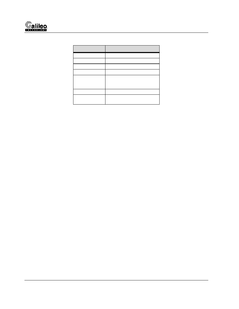
GT-64111 System Controller for RC4640, RM523X and VR4300 CPUs
52
Revision 1.0
TABLE 20. DevNum to IdSel Mapping
The CPU/Local Master accesses the GT-64111's internal configuration registers when the fields DevNum and BusNum
in the Configuration Address register are equal to `0'. The GT-64111 configuration registers are also accessed from the
PCI bus when the GT-64111 is a target responding to PCI configuration read and write cycles.
Note: The CPU/Local Master interface unit cannot distinguish between an access to the GT-64111 PCI configuration
space and an access to an external PCI device configuration space. This is because both are accessed using an
access to the GT-64111 internal space (i.e. Configuration Data register). When the CPU/Local Master is operating in
big-endian mode, any access to the GT-64111 internal space undergoes byte swapping as all internal registers are lit-
tle-endian. With the CPU/Local Master operating in big-endian mode and the PCI ByteSwap bit (bit [0] @ 0xc00) set to
`0' (i.e., swap bytes), bytes will be swapped once for PCI configuration accesses intended for the GT-64111 configura-
tion space but will be swapped twice for PCI configuration accesses intended for devices external to the GT-64111.
This requires the software to format write data and interpret read data differently for PCI configuration accesses to the
GT-64111's registers and configuration accesses through the GT-64111 to an external device.
IMPORTANT:
The configuration enable bit (ConfigEn) in the Configuration Address register must be set before the
Configuration Data register is read or written. Failure to do this will "lock up" the GT-64111 and require a RESET to
recover.
6.4.1
Special Cycles and Interrupt Acknowledge
A Special cycle is generated whenever the Configuration Data register is written to while the Configuration Address
register has been previously written with `0' for BusNum, `1f' for DevNum, `7' for FunctNum and `0' for RegNum.
An Interrupt acknowledge cycle is generated whenever the Interrupt Acknowledge (0xc34) register is read.
6.5
Target Configuration and Plug and Play
The GT-64111 includes all of the required plug and play PCI configuration registers. These registers, as well as the GT-
64111's internal registers, may be accessed from both the CPU/Local Master and the PCI bus.
The GT-64111 acts as a two function device when being configured from the PCI bus. The base address registers
available in Function 0 are used to decode accesses for which there is no byte swapping; Function 1 is used to decode
byte swapped addresses. All other registers are shared between Function 0 and Function 1.
6.5.1
Plug and Play Base Address Register Sizing
Systems adhering to the plug and play configuration standard determine the size of a base address register's decode
range by first writing 0xFFFF.FFFF to the BAR, then reading back the value contained in the BAR. Any bits that were
unchanged (i.e. read back a zero) indicate that they cannot be set and are therefore not part of the address compari-
son. With this information the size of the decode region can be determined.
1
The GT-64111 responds to BAR sizing requests based on the values programmed into the Bank Size Registers. These
DevNum[15:11]
PAD[31:11]
00001
0 0000 0000 0000 0000 0001
00010
0 0000 0000 0000 0000 0010
00011
0 0000 0000 0000 0000 0100
00100
0 0000 0000 0000 0000 1000
-
-
-
-
-
-
10101
1 0000 0000 0000 0000 0000
00000,
10110 - 11111
0 0000 0000 0000 0000 0000

GT-64111 System Controller for RC4640, RM523X and VR4300 CPUs
Revision 1.0
registers can be loaded automatically after RESET from the system ROM (see below).
6.5.2
Multi-Function Device, Swap BARs
If one of the Swap Base Address Registers is enabled after Rst* (see Reset Configuration), the GT-64111 will be con-
figured as a multi-function device (bit 7 in the Header Type register set to 1, 0xe). To access any of the Swap Base
Address Registers, a configuration access addressed to function #1 should be used with the appropriate register offset.
If a different offset other than 0x010, 0x014, or 0x01c is accessed when specifying function #1, the transaction will
access the corresponding offset register in function #0. Configuration transactions to any other function number will be
ignored.
If none of the Swap Base Address Registers are enabled after Rst*, the GT-64111 will be configured as a single func-
tion device (bit 7 in the Header Type register set to 0, 0xe) and the function #1 configuration registers will be unaccess-
able.
Note: If the GT-64111 is programmed as a single function device, the Swap Base Address Registers can still be pro-
grammed by a configuration access addressed to function #1 and the appropriate register offset. But, any PCI access
which is a hit in these Swap Base Address Registers will be ignored by the GT-64111.
6.5.3
PCI Autoconfiguration at RESET
Eight PCI registers can be automatically loaded after Rst*. Autoconfiguration mode is enabled by asserting the
DMAReq[3]* LOW on Rst*. Any PCI transactions targeted for the GT-64111 will be retried while the loading of the PCI
configuration registers is in process.
It is highly recommended that all PC applications utilize the PCI Autoconfiguration at RESET feature. The auto-
load feature can be easily implemented with a very low cost EPLD. Galileo provides sample EPLD equations upon
request. (You can always pull the EPLD off your final product if you find there are no issues during testing.)
NOTE: The GT-64111's default Class Code is 0x0580 (Memory Controller) which is a change from the GT-64011.
The GT-64011 used the Class Code 0x0600 which denotes Host Bridge. Some PCs refuse to configure host bridges if
they are found plugged into a PCI slot (ask the BIOS vendors why...). The "Memory Controller" Class Code does not
cause a problem for these non-compliant BIOSes, so we used this as the default in the GT-64111. The Class Code
can be reporgrammed in both devices via autoload or CPU register writes.
1. Please refer to the PCI specification for more information on the BAR sizing process.

GT-64111 System Controller for RC4640, RM523X and VR4300 CPUs
54
Revision 1.0
The PCI register values are loaded from the ROM controlled by BootCS* are shown in Table 21, below.
TABLE 21. PCI Registers Loaded at RESET
6.5.4
Expansion ROM Functionality
The GT-64111 implements the PCI Expansion ROM as required by PC boot devices. The PCI Expansion ROM func-
tionality is enabled by strapping DAdr[2] low at RESET ( see Reset section.)
If the PCI Expansion ROM is disabled, expansion ROM register (offset 0x30 of PCI configuration space) acts as
reserved register and returns all `0's when read.
When the expanion ROM is enabled by the pin strapping option, the PCI Expansion ROM BAR appears magically in
the GT-64111's PCI configuration header. However, the Expansion ROM decoder shares functionality with the CS3*/
BootCS* resource. In normal operation (i.e. after the BIOS initialization is complete), the Expansion ROM is disabled
via bit 0 in the Expansion ROM BAR. During BIOS boot, however, the BIOS "turns on" the Expansion ROM decoder by
setting bit 0. When the Expansion ROM decoder is "on" the following happens:
∑
The PCI target will act as if the Timeout0 and Timeout1 MSBs are `1' (which means initial value of 0x8f and
0x87 respectively). This is done to allow for the long default access time from 8-bit boot ROMs.
∑
The Device unit will bypass it's address decoding for ALL transactions from PCI that are targeted to expansion
ROM or CS[3]/BootCS* . All of these transactions will assert CS[3] regardless of the actual address.
∑
The GT-64111 will act this way as long as bit[0] of expansion ROM register is set to 1 (it's the BIOS responsibil-
ity to clear this bit when it is done executing/probing the Expansion ROM. (If for any reason the BIOS does not
clear bit[0] of expansion ROM BAR, you can still program this bit to 0 from CPU/Local Master side.)
6.6
PCI Parity Support
GT-64111 implements all parity features required by PCI spec, including PAR,PERR* and SERR* generation and
checking.
As an initiator, GT-64111 generates even parity on PAR signal for address phase and data phase of write transaction. It
samples PAR on data phase of read transaction. If it detects bad parity and PErrEn bit in Status and Command config-
uration register is set, it asserts PERR*.
As a target, GT-64111 generates even parity on PAR signal for data phase of a read transaction. It samples PAR on
address phase and data phase of write transaction. If it detects bad parity and PErrEn bit in Status and Command con-
figuration register is set, it asserts PERR*.
GT-64111 might asserts SERR* if one of the following conditions occur:
∑
Detect bad address parity as a target
∑
Detect bad data parity on a write transaction as a master (detects PERR* asserted)
∑
Detect bad data parity on a read transaction as a master
∑
Detect ECC error on read from SDRAM or Device
∑
Performs master abort
Register
Offset
Boot Device
Address
Device and Vendor ID
0x000
0x1fffffe0
Class Code and Revision ID
0x008
0x1fffffe4
Subsystem Device and Vendor ID
0x02c
0x1fffffe8
Interrupt Pin and Line
0x03c
0x1fffffec
RAS[1:0]* Bank Size
0xc08
0x1ffffff0
RAS[3:2]* Bank Size
0xc0c
0x1ffffff4
CS[2:0]* Bank Size
0xc10
0x1ffffff8
CS[3]* & Boot CS* Bank Size
0xc14
0x1ffffffc

GT-64111 System Controller for RC4640, RM523X and VR4300 CPUs
Revision 1.0
∑
Detect target abort
SERR* will be asserted if SErrEn bit in
Status and Command configuration register is set to 1 and if SERR* is not
masked through
SERR Mask register.
6.7
PCI Bus/Device Bus/CPU/Local Master Clock Synchronization
The PCI interface is designed to run asynchronously with respect to the AD and CPU/Local Master buses. The syn-
chronization delay between these two clock domains can be reduced, however, by running the interfaces in synchro-
nized mode. An example would be having the CPU/Local Master/AD buses running at 66MHz and the PCI bus running
at a 33MHz frequency that was derived from the 66MHz.
Latency through the GT-64111 is reduced to a minimum when synchronized mode is selected. The synchronization
mode is set via the SyncMode bits in the PCI Internal Command register (0xc00).
Note: PClk frequency must be smaller than TClk frequency by at least 1MHz. Please see AC Timing section for more
information.
6.8
66MHz Capability Bit
The 66MHz capability bit in the PCI header is sampled from an external pin at RESET. Note that the state of this bit
does not in any way affect the speed of the PCI interface. It only acts as an "advertisement" to other PCI devices
(or the host CPU) that the GT-64111 is capable of running at 66MHz.
Please see the RESET strapping options section for more details.
6.9
Universal PCI Vio Pin
The Vio pin is used by the GT-64111 to determine the signalling voltage of the PCI interface (3.3V or 5V). This pin is
normally connected to pin 88 on side B of a standard PCI connector when used in a PCI add-in card application.
NOTE: The Vio pin on the GT-64111 was used as the Vref pin on the GT-64011. Vref is used on the GT-64011 to
set the voltage for the CPU interface to be either 3.3V or 5V.
6.10
PCI Interface Restrictions
Note: No PCI access should be attempted before 6 PClk cycles following deassertion of Rst* have expired.
6.10.1 Master
a)
Latency count, as specified in LatTimer (PCI Configuration Register 0x00c), should not be programmed to less
than 6.
6.10.2 Slave
a)
The set bits in the Bank Size registers must be sequential.
b)
When the slave is locked, in order to prevent a deadlock, all transactions to internal registers (I/O or memory
cycles) are not supported (retry will be issued).
c)
Timeout0 (PCI Internal register 0xc04), should not be programmed to less than 2.
6.10.3 Master and Slave
a)
PClk frequency must be smaller than TClk frequency by at least 1MHz.

GT-64111 System Controller for RC4640, RM523X and VR4300 CPUs
56
Revision 1.0
7.
DMA Controller
The GT-64111's DMA Controller consists of four independent channels. The DMA channels are used to optimize sys-
tem performance by moving large amounts of data without CPU intervention. Rather than having the CPU read data
from one source and write it to another, each DMA channels can be programmed to automatically transfer data inde-
pendent of the CPU. This frees the CPU and allows it to continue executing other instructions simultaneous to the
movement of data.
Each DMA channel can move data between DRAM and devices, between devices on the PCI bus, or between DRAM
and devices, and devices on the PCI bus. The four DMA channels request to execute a DMA and if there are simulta-
neous requests, a programmable arbiter which DMA channel will be serviced (see Section 7.5 for more information
about the DMA Arbiter). All DMA transfers use an internal 32-byte FIFO for moving data (see Figure 24). Data is trans-
ferred from the source into the internal FIFO, and from the internal FIFO to the destination. Each DMA channel can be
programmed to move up to 64 KBytes of data per transaction. The burst length of each transfer of DMA can be set
from 1 to 32 bytes. Accesses can be non-aligned both in the source and the destination.
Figure 24: DMA Controller
DMA FIFO
8 x 32 bit
D M A
Arbiter
Byte Count 0
Source Address 0
Destination Address 0
Pointer to Next Record 0
Byte Count 1
Source Address 1
Destination Address 1
Pointer to Next Record 1
Byte Count 2
Source Address 2
Destination Address 2
Pointer to Next Record 2
Byte Count 3
Source Address 3
Destination Address 3
Pointer to Next Record 3
DATA 7
DATA 6
DATA 5
DATA 4
DATA 3
DATA 2
DATA 1
DATA 0
C h a n n e l 0
C h a n n e l 1
C h a n n e l 2
C h a n n e l 3
DRAM/Device Controller
PCI
D R A M / D e v i c e
Source Data
PCI Source Data
DRAM/Device Controller
PCI
PCI Destination
Data
D R A M / D e v i c e
Destination Data
Read Data from
Soruce Address
Write Data to
Destination Address
GT-64111 System Controller for RC4640, RM523X and VR4300 CPUs
Revision 1.0
7.1
DMA Channel Registers
Each DMA Channel record consists of the following data fields which can be written by the CPU, PCI, or DMA control-
ler in the process of fetching a new record from memory:
∑
Byte count (0x800 - 0x80c). This register is programmed with a 16-bit number which contains the number of
bytes of data that this channel must DMA. The maximum number of bytes which a the DMA channel can be
configured to transfer is 64K. This register will decrement at the end of every burst of transmitted data from
source to destination. When the byte count register is 0, the DMA transaction is finished.
∑
Source address (0x810 - 0x81c). This register is programmed with a 32-bit address. This is the source
address for data and can be from the DRAM, Device or from PCI. This register will either increment, decre-
ment, or hold the same value according to bits 3:2 of the Channel Control Register (see Section 7.2.2).
∑
Destination address (0x820 - 0x82c). This register is programmed with a 32-bit address. This is the destina-
tion address for data and can be to the DRAM/Device or to PCI. This register will either increment, decrement,
or hold the same value according to bits 5:4 of the Channel Control Register (see Section 7.2.3).
∑
Pointer to the next record (0x830 - 0x83c). The register contains a 32-bit address where the values for the
next DMA Channel record can be loaded for chained operation. This can be from the DRAM/Device controller
or from PCI. The byte count, source address, and destination address must be located at sequential
addresses. This register is only used when the channel is configured for Chained Mode (see Section 7.2.5). A
value of `0' (NULL) for this register indicates this is the last record in the chain. See below for more information
about Chained DMA mode.
7.2
DMA Channel Control Register (0x840 - 0x84c)
Each DMA Channel has its own unique Control Register where certain DMA modes can be programmed. Following are
the bit descriptions for each field in the control register.
7.2.1
AddControl[1:0], GT-64111-P-1 ONLY
AddControl[1:0] are for Source and Destination address control for PCI devices (regardless of the CPU Interface unit's
address decoding). In other words, the DMA will access PCI Memory regardless of the results of the address decoding
in the CPU Interface unit if the proper bit is set.
TABLE 22. Setting AddControl[1:0]
7.2.2
SrcDir, bits[3:2]
The SrcDir field contains information about how the source address for the DMA transfer is handled. These bits, if set
to `00' (default), will automatically increment the source address. If set to `01', the source address will automatically
decrement. If set to `10', the source address will remain constant throughout the DMA burst. `11' is a reserved setting
and these bits must not be set to this value.
7.2.3
DestDir, bits[5:4]
The DestDir field contains information about how the destination address for the DMA transfer is handled. These bits, if
set to `00' (default), will automatically increment the destination address. If set to `01', the destination address will auto-
matically decrement. If set to `10', the destination address will remain constant throughout the DMA burst. `11' is a
reserved setting and these bits must not be set to this value.
AddControl[0]
AddControl[1]
Source
Destination
0
0
CPU Address Space
CPU Address Space
1
0
PCI Memory Space
CPU Address Space
0
1
CPU Address Space
PCI Memory Space
1
1
PCI Memory Space
PCI Memory Space
GT-64111 System Controller for RC4640, RM523X and VR4300 CPUs
58
Revision 1.0
7.2.4
DatTransLim, bits[8:6]
The DatTransLim field contains the burst limit of each data transfer. The burst limit can vary from 1 byte to 32 bytes in
modulo-2 steps (i.e. 1, 2, 4,..., 32) as shown in Table 23.
TABLE 23. Setting DataTransLim
7.2.5
ChainMod, bit 9
ChainMod determines whether this channel is set in chained mode or not. The default setting of `0' enables chained
mode for the channel. Therefore, at the completion of a DMA transaction, the Pointer to Next Record Register provides
the address of a new DMA Record. If this register contains a value of `0' (NULL), this indicates that this is the last
record in the chain.
In chained mode (bit 9 set to 0), a channel can be enabled by two different methods.
1.
The channel record's parameters for the current transaction (Byte Count, Source, Destination, and Next Record
Pointer) should be initialized in DRAM/Device memory space or PCI devices. The address of the first record should
be initialized by writing it to the Next Record Pointer Register of the channel. The channel should be enabled by
setting ChanEn to `1' (see Section 7.2.8), and setting FetNexRec (see Section 7.2.9) to `1'. Setting these two bits
can be completing during the same write or FetNexRec should be set to `1' on the first write and then the DMA can
be initiated by setting ChanEn to '1' on another write. If in block mode, the DMA will start once the particular chan-
nel has been arbitrated for. If in demand mode, the DMAReq* must be asserted and then the DMA will start once
the particular channel has been arbitrated for.
2.
The channel's record's parameters for the current transaction (Byte Count, Source, Destination, and Next Record
Pointer) should be initialized in the proper DMA Channel Registers. In block mode, the DMA can be initiated by set-
ting ChanEn to '1' and the DMA will start once the particular channel has been arbitrated for. If in demand mode,
the DMAReq* must be asserted and then the DMA will start once the particular channel has been arbitrated for.
Fetching the data for the next record (i.e. loading Byte Count, Source, Destination, and Next Record Pointer registers)
is not dependent on DMAReq*. This action will occur automatically as long as the channel is enabled and FetNexRec
is set to `1' or the Byte Count has reached a terminal count and the Next Record Pointer is not NULL.
See Figure 25 for a diagram of chained mode DMA. If ChainMod is set to `1', chained mode is disabled. Note that in
non-chained mode the Byte Count, Source, and Destination Registers should be initialized prior to enabling the chan-
nel.
7.2.6
IntMode, bit 10
IntMode controls when this channel asserts the DMAComp (DMA Complete) Interrupt. The default setting of `0' sets the
channel to assert the DMAComp Interrupt every time the DMA byte count reaches 0. If the channel is set to chained
mode, and IntMode is set to `1', the DMAComp Interrupt will only be asserted when both the Pointer to Next Record
Register has a NULL value and Byte Count is 0. If chained mode is disabled, the setting of IntMode is irrelevant and
DMAComp Interrupt will be asserted every time the Byte Count reaches 0.
Bits 8:6
Transfer Limit of each DMA Access
101
1 Byte
101
2 Bytes
000
4 Bytes
001
8 Bytes
011
16 Bytes
111
32 Bytes

GT-64111 System Controller for RC4640, RM523X and VR4300 CPUs
Revision 1.0
7.2.7
TransMod, bit 11
TransMod indicates whether the channel is set to operate in demand mode or block mode. The default setting of `0' set
the channel to operate in demand mode where DMA accesses are initiated by externally asserting one of the four
DMAReq[3:0]* pins. If TransMod is set to `1', the channel is set to operate in block mode where DMA accesses are ini-
tiated by setting ChanEn, Bit 12. In Block mode, the DMAReq* lines are ignored.
7.2.8
ChanEn, bit 12
ChanEn can enable or disable the DMA channel. When ChanEn is set to `0', the channel is disabled. When ChanEn is
set to `1', the DMA is initiated based on the current setting loaded in the channel record (i.e. Byte Count, Source
Address and Destination Address).
Note that the DMA channel can be enabled or disabled via ChanEn if the channel is
in Demand or Block Mode.
7.2.9
FetNexRec, bit 13
FetNexRec is a field which is only meaningful when chained mode is enabled for the channel. Setting this bit to `1' will
force a fetch of the next record based on the value in the Pointer to Next Record Register. This bit can be set even if the
current DMA has not yet completed. This bit is reset back to `0' after the fetch of the new record is complete.
7.2.10 DMAActSt, bit 14 (Read Only)
DMAActSt is a read only field and can be polled to see the DMA activity status of the channel. If this bit is set to `0', the
channel is not active. If this bit is set to `1', the channel is active.
Figure 25: Chained Mode DMA
7.3
Restarting a Disabled Channel (previously active)
In Non-Chained mode, ChanEn should be set to `1'.
GT-64010 Channel 0 DMA Registers
Byte Count (ByteCt)
Source Address (SrcAdd)
Destination Address (DestAddr)
Next Record Pointer (NextRecPtr): 0x10
ByteCt
SrcAdd
DestAddr
NextRecPtr: 0x100
0x10
0x14
0x18
0x1c
x
x
x
x
0x100
0x104
0x108
0x10c
Transfer #1
Transfer #2
Transfer #n
ByteCt
SrcAdd
DestAddr
NextRecPtr: y
ByteCt
SrcAdd
DestAddr
NULL Pointer: 0x0

GT-64111 System Controller for RC4640, RM523X and VR4300 CPUs
60
Revision 1.0
In Chained mode, the software should find out if the first fetch took place. If it did, only ChanEn should be set to `1'. If it
did not, the FetNexRec should also be set to `1'.
7.4
Reprogramming an Active Channel
To reprogram an active channel, the channel should first be disabled by setting ChanEn to `0'. Then it must be assured
that the channel is no longer active (for example by polling the DMAActSt of the channel). New DMA parameters
should be programmed prior to re-enabling the channel via setting ChanEn to `1'.
7.5
Arbitration
The DMA controller has a programmable arbitration scheme between its four channels. The channels are grouped into
two groups, one group includes channel 0 and 1, and the other group includes channels 2 and 3. The channels in each
group can be programmed to have priority so that a selected channel has the higher priority, or to have the same prior-
ity in round robin. The priority between the two groups can be programmed in a similar way so that a selected group
has a higher priority, or to have the same priority in round robin. The priority scheme has additional flexibility with the
programmable Priority Option. With the Priority Option the DMA bandwidth allocation can be divided in a fairer way. For
example, if the PrioOpt bit is set to `0' and the PrioGrps field is set as `10', the requesting devices will get the DMA in
the order 0,1,2,0,1,3,0,1,2,0,1,3,..... (assuming that PrioChan1/0 and PrioChan3/2 are set to round robin), while if the
PrioOpt bit is set to `1' the requesting devices will get the DMA in the order 0,1,0,1,0,1,2,3,2,3,2,3,..... The DMA arbiter
control register can be reprogrammed any time regardless of the channels' status (active or not active).
Some arbitration examples follow to facilitate the understanding of this register are shown in Table 24.
TABLE 24. Channel Arbitration Examples
7.6
DMAReq[3:0]*
The DMAReq[3:0]* input pins are asserted by an external device to request a DMA transfer in Demand mode. The
DMAReq* should be asserted as long as the transfer initiator has at least DataTransLim of bytes to provide (in case
that it is the source) or as long as it has space to absorb at least DataTransLim of bytes (in case that it is the destina-
tion). The DMAReq* should be deasserted by the source when the transfer initiator sees that it does not have at least
DataTransLim of bytes to provide (i.e. FIFO empty). DMAReq* should also be deasserted by the destination when the
it does not have enough space to absorb at least DataTransLim of bytes (i.e. FIFO full) AND DMAAck* is asserted
LOW.
# of Requesting
Channel
E x a m p l e
C h a n n e l s
Arbiter Control
Register Value
C h a n n e l S e r v i c e O r d e r
4
All
0x40
0,2,1,3,0,2,1,3,.....
4
All
0x0
0,1,2,3,0,1,2,3,.....
3
0,1,2
0x40
0,2,1,2,0,2,1,2,.....
3
0,1,2
0x0
0,1,2,0,1,2,0,1,2,.....
4
All
0x45
1,3,1,3,1,3,.....,0,2,0,2,0,2,......
4
All
0x5
1,0,3,2,1,0,3,2,1,0,3,2,.....
3
0,1,2
0x45
1,2,1,2,1,2,.....,0,0,0,0,0,0,.....
3
0,1,2
0x5
0,1,2,0,1,2,.....
4
All
0x55
3,3,3,3,3,3,2,2,2,2,2,1,1,1,1,0,0,0,......
4
All
0x15
3,2,1,3,2,0,3,2,1,3,2,0,.....
3
0,1,2
0x55
2,2,2,2,1,1,1,1,0,0,0,0,.....
3
0,1,2
0x15
2,1,2,0,2,1,2,0,.....
3
0,2,3
0x55
3,3,3,...,2,2,2,...,0,0,0,.....
3
0,2,3
0x15
3,2,0,3,2,0,3,2,0,.....

GT-64111 System Controller for RC4640, RM523X and VR4300 CPUs
Revision 1.0
The DMAReq* is sampled on every clock cycle but it influences arbitration only in the DMA arbitration cycle or when all
channels are idling. The DMA arbitration cycle is the cycle in which the destination unit inside the GT-64111 acknowl-
edges the last written data from the DMA unit.
7.7
DMAAck[3:0]*
The DMAAck[3:0] output pins are asserted by the GT-64111 to indicate that a current DMA request is being serviced.
The DMAAck* is asserted only when the GT-64111 accesses a Device. It is asserted when ALE is asserted and should
be qualified with CSTiming*.
7.8
Design Information
The following sections contain more detailed information about designing with GT-64111's DMA Controller. The follow-
ing definitions are used throughout this section:
1.
Device: A device located on the memory bus mapped to one of the GT-64111's Chip Selects (including BootCS).
2.
PCI Agent: Any device located on the PCI bus.
3.
DRAM: DRAM memory located on the memory bus.
7.8.1
DMA in Demand Mode
Demand mode is especially designed for transferring data between Memory (Device, DRAM, PCI agent) and a Device.
This is because the DMAAck* is asserted only when the GT-64111 is accessing a Device. In this mode the transfer ini-
tiator (usually a Device) asserts DMAReq* to signal the GT-64111 that a new DMA transfer should begin. As an
acknowledgment response, the GT-64111 asserts the DMAAck* to signal that the asserted DMAReq* is currently being
processed.
In each DMA transfer, the DMA attempts to read the amount of DataTransLim from the source address and writes it to
destination address. In the source direction, at the beginning and end of the DMA, there may be less than DataTrans-
Lim transfers if the address is not aligned or the remaining Byte Count to be transferred is smaller then the DataTrans-
Lim. In the destination direction, the DMA writes all data that was read from the source to the destination. This may
happen in two DMA accesses if the destination address is not aligned.
The channel will stay active until the Byte Count reaches the terminal count or until the CPU disables the channel. Note
that if the DMAReq* is always asserted, then this is equivalent to transfer data in Block Mode.
7.8.1.1
DemandMode DMA examples/recommendations
Source: DRAM/PCI, Destination: DRAM/PCI
In Demand mode, then DMAAck* should be externally generated (i.e. polling accesses of the GT-64111 to certain
addresses). Typically, in this case it is better to use BlockMode because Memory is typically always ready and
DMAAck* is NEVER asserted.
Source: Device, Destination: DRAM or PCI
The Device transfer initiator asserts DMAReq* when it has at least DataTransLim number of bytes to provide. It should
deassert the DMAReq* when no more data is ready and DMAAck* is asserted. Even if another master (like a PCI mas-
ter) drives the DMAReq* then the DMAAck* can signal to that master that the GT-64111 is currently accessing the
device for read. Note that DMAAck* must always be qualified with CSTiming*.
Source: DRAM or PCI, Destination: Device
The Device transfer initiator asserts a DMAReq* when it can absorb DataTransLim number of bytes to be written to it.
Even if another master drives the DMAReq* then the DMAAck* can signal the master that the GT-64111 is currently
accessing the device for write.

GT-64111 System Controller for RC4640, RM523X and VR4300 CPUs
62
Revision 1.0
7.8.2
DMA in Block Mode
In block mode no hand shake signals are used to initiate DMA transfers. The DMA unit will complete the transfer once
the CPU has programmed the DMA and enabled it.
7.8.3
Non-Chain Mode
In non-chain mode the CPU or PCI master initiates the DMA channel parameters (Source, Destination Byte Count and
command Registers).The DMA will start to transfer data after the enable bit in the Command register is set to 1. The
DMA remains in an active state until the Byte Count reaches a terminal count or until the channel is disabled.
7.8.4
Chain Mode
In chain mode the DMA channel parameters (Source, Destination Byte Count and Pointer to Next Record) are read
from records located in Memory, Device or PCI. The DMA channel stays in the active state until Pointer to Next Record
is NULL and the Byte Count reaches the terminal count. In this mode, an interrupt can be asserted every time the byte
count reaches the terminal count or when BOTH the Byte Count reaches the terminal count and the Pointer to Next
Record is NULL.
7.8.5
Dynamic DMA chaining
Dynamic chaining is when DMA records are added to a chain which a DMA channel is actively working on. The main
issue is to synchronize between when the GT-64111 reads the last chain record (the NULL pointer) to the time the CPU
changes the current last DMA record. Following is an algorithm which provides this synchronization mechanism.
1.
Prepare the new record.
2.
Change the last record's Pointer to Next Record to point to the new record.
3.
Read the DMA control register.
If the DMAActSt bit is 0 (NOT active) {
Update the Pointer to Next Record in the GT-64111 and assert the FetNexRec bit
}
else {
read the Pointer to Next Record GT-64111. If it's equal to NULL {
Mark (by using a flag or something) that in the next DMA chain complete interrupt you'll need to -
[[[[{
Update the NRP register in the GT-64010 and Write the Fetch Next Record }]]]]
}
}
7.9
DMA Restrictions
1.
Transfers of less than 4 bytes are not supported.
2.
When Source or Destination address is decremented, both addresses should be word-aligned (that is, A1 and A0
should be both zero), and Byte Count should be a multiple of 4 (this applies for burst limits greater than 4 bytes).
3.
When the burst limit is less than 4 bytes, no decrement mode (source or destination) is not supported.

GT-64111 System Controller for RC4640, RM523X and VR4300 CPUs
Revision 1.0
4.
When using the address hold option in the source direction (see Section 7.2.2), the source address should keep
the following rules:
∑
word-aligned if burst limit is greater or equal to 4 bytes.
∑
bits [1:0] equal to 00, 01 or 10 if burst limit is equal to 2 bytes.
∑
no restriction for burst limit equal to 1 byte.
5.
When using the address hold option in the destination direction (see Section 7.2.3), the following rules should be
kept:
∑
both Source and Destination addresses should be word-aligned if burst limit is greater or equal to 4 bytes.
∑
bit [0] of both Source and Destination addresses should be equal to 0 if burst limit is equal to 2 bytes.
∑
no restriction for burst limit equal to 1 byte.
6.
Fly-by transfers are not supported.
7.
Records' addresses must be a multiple of 16 bytes.
8.
If the destination is a device and if DataTransLimit is smaller or equal 4 bytes, the DMAAck* asserts during the
same cycle as the arbitration cycle. Therefore, DMAReq*, which is typically de-asserted based on the assertion of
DMAAck*, is NOT seen in the DMA arbitration cycle. So although the device does not want to be accessed, a new
transfer may begin.
∑
If DataTransLimit is bigger then 4 bytes then there is no problem. In this case, it is recommended to have a
device that can accepts bursts.
∑
A solution when using one channel only and DataTransLim is less equal to 4 is as follows:
∑
STATE A: The first request should be issued after the channel is enabled and the Device has enough room for
DataTransLim. DMAReq* should be asserted for 1 cycle and then deasserted.
∑
STATE B: While DMAAck* is asserted, if the Device has enough room for data, assert the DMAReq* for 1 cycle
and then deassert the request. Remain in STATE B. If the Device has no room for data then do not assert the
DMAReq*. Go to STATE A.
∑
For 16-bit devices, use 4 byte source aligned addresses for data in DRAM, and Device destination addresses
aligned to 4 bytes + 2 while DataTransLim = 4 bytes.

GT-64111 System Controller for RC4640, RM523X and VR4300 CPUs
64
Revision 1.0
8.
Timer/Counters
There are three 24-bit wide and one 32-bit wide timer/counter on the GT-64111. Each one can be selected to operate
as a timer or as a counter. In Counter mode, the counter will count down to terminal count, will stop and issue an inter-
rupt. In Timer mode, it will count down, will issue an interrupt on terminal count, and will reload itself to the programmed
value and continue to count. Reads from the counter or timer are done from the counter itself, while writes are to its
register. For example, note that even though the registers are programmed to an initial value of `0' the counters will
read 0xffffff. In order to reprogram a timer/counter, it should first be disabled, then it should be loaded with a new value
and after that it should be enabled as appropriate (counter or timer).
NOTE: There are no external input pins for enable/disable nor are there any output timer pins on the GT-64111.

GT-64111 System Controller for RC4640, RM523X and VR4300 CPUs
Revision 1.0
9.
Interrupt Controller
The GT-64111 includes an interrupt controller that routes internal interrupt requests to both the CPU/Local Master and
the PCI bus.
The interrupt controller ORs all internal interrupt sources and asserts an interrupt to the CPU/Local Master or to the PCI
when one or more internal interrupts are asserted. There is one Cause register and two Mask registers. The Cause
register has one bit for each interrupt source. If the source asserts an interrupt, its respective bit in the Cause register
will be set. This bit can be read by the CPU/Local Master or from the PCI bus.
The interrupt is acknowledged by the CPU/Local Master or by the PCI bus by resetting its bit in the Cause register (writ-
ing zero to the specific bit and one to all other bits). ONE EXCEPTION for the above is the CPUInt ([25:21] and PCIInt
([29:26])) which are used by the PCI to generate interrupt to the CPU and vice versa. These are SET by writing zero
from the interrupt originating side and CLEARED by writing zero from the interrupt destination side. Each interrupt
source has one mask bit in the CPU/Local Master Mask register and one bit in the PCI Mask register. A zero in the
CPU/Local Master Mask register bit will mask the interrupt from asserting an interrupt to the CPU/Local Master. A zero
in the PCI Mask register bit will mask the interrupt from asserting an interrupt to the PCI.
IntSum in the Interrupt Cause register is the logical OR of bits[29:1], regardless of the Mask registers' values. This is in
order to be notified via polling if any interrupt occurred within the GT-64111. Therefore, bit[0] of both the CPU/Local
Master Mask and PCI Mask registers is read-only `0'.
CPU/Local Master IntSum in the Interrupt Cause register is the logical OR of bits[29:26,20:1], masked by
bits[29:26,20:1] of the CPU/Local Master Mask register. Therefore, bits[25:21] of the CPU/Local Master Mask register,
being non-relevant to interrupts directed to the CPU/Local Master, are read-only `0'. Also bits[31:30], being summaries,
are read-only `0'.
PCIIntSum in the Interrupt Cause register is the logical OR of bits[25:1], masked by bits[25:1] of the PCI Mask register.
Therefore, bits[29:26] of the PCI Mask register, being non-relevant to interrupts directed to the PCI, are read-only `0'.
Also bits[31:30], being summaries, are read-only `0'.

GT-64111 System Controller for RC4640, RM523X and VR4300 CPUs
66
Revision 1.0
10.
Reset Configuration
The GT-64111 must acquire some knowledge about the system before it is configured by the software. Special modes
of operation are sampled on RESET in order to enable the GT-64111 to function as required. Certain pins must be
pulled up or down (4.7K Ohm recommended) externally to accomplish this. The following configuration pins are contin-
uously sampled from Rst* assertion until 3 TClk cycles after Rst* is deasserted.
P i n
C o n f i g u r a t i o n F u n c t i o n
Interrupt*:
Endianess
0 -
1 -
Big endian data format
Little endian data format
DAdr[11:10]:
Device Boot Bus Width
00 -
01 -
10 -
11 -
8 bits
16 bits
32 bits
64 bits
DAdr[9]:
LEAdrE/DMAReq[2]* Selection
0 -
1 -
DMAReq[2]*
LEAdrE
DAdr[8]:
OEB Polarity
0 -
1 -
Active LOW
Active HIGH
DAdr[7]:
External Latches Presence
0 -
1 -
Latches are present
System without latches
DAdr[6]:
Enable/DisableCS[2:0] PCI BAR for address matching and size
response
0 -
1 -
Enable
Disable
DAdr[5]:
DMAReq[1]*/ParErr* Selection
0 -
1 -
DMAReq[1]* (no parity)
ParErr*
DAdr[4]:
DMAReq[0]*/Ready* Selection
0 -
1 -
Ready*
DMAReq[0]*
DAdr[3]:
Enable/disable CS[3] & BootCS PCI BAR for address matching
and size response
0 -
1 -
Enable
Disable

GT-64111 System Controller for RC4640, RM523X and VR4300 CPUs
Revision 1.0
NOTES:
1. DAdr[9] should be pulled LOW whenever LEAdrE is not used in the system (e.g., DRAM is not operating in decre-
ment mode).
2. If Autoload enable is sampled low during reset, device and vendor ID[31:0], class code and revision ID[31:0], Sub-
system ID and Subsystem Vendor ID[31:0], Interrupt Pin, Interrupt Lines[15:0], RAS[1:0]* Bank Size, RAS[3:2]* Bank
Size, CS[2:0]* Bank Size, CS[3] & BootCS* Bank Size will be autoloaded starting from address 0x1FFF.FFE0.
3. If either DAdr[1] or DAdr[0] is sampled `0' on Rst*, the GT-64111 will be initialized as a multi-function device (bit 7 in
the Header Type register set to 1, 0xe).
4. If a PCI BAR is disabled for address matching and size response, a PCI configuration read to this register will return
0x0. PCI configuration writes to this BAR will remain valid (i.e. the value of the configuration write will remain in the reg-
ister). But, if a disabled BAR is programmed with a base address, and there is a PCI address on the PAD[31:0] bus
which hits in the disabled BAR, the GT-64111 will ignore this transaction as if there was NO hit (i.e. DevSel* will NOT
1. This pin was a Vss on the GT-64011.
DAdr[2]:
Enable PCI Expansion ROM
0 -
1 -
Enable
Disable
DAdr[1]:
Enable/Disable Swapped RAS[3:2] PCI BAR for address match-
ing and size response
0 -
1 -
Enable
Disable
DAdr[0]:
Enable/Disable Swapped CS[3] & Boot CS PCI BAR for address
matching and size response
0 -
1 -
Enable
Disable
DMAReq[3]*:
Autoload Enable
0 -
1 -
Enable
Disable
DMAReq[1]*/
ParErr*:
Enable/Disable internal registers I/O mapped PCI BAR for
address matching and size response
0 -
1 -
Enable
Disable
DMAReq[0]*/
Ready*:
Enable/Disable RAS[3:2] PCI BAR for address matching and size
response
0 -
1 -
Enable
Disable
Pin 15:
Enable 66MHz PCI Bus Capability in PCI Header
1
0 -
1 -
33MHz PCI Bus Operation Indicated
66MHz PCI Bus Operation Indicated
P i n
C o n f i g u r a t i o n F u n c t i o n

GT-64111 System Controller for RC4640, RM523X and VR4300 CPUs
68
Revision 1.0
be asserted).
5. If a PCI BAR is disabled for address matching and size response, a BIOS query of this disabled BAR for its size will
respond with 0x0. In other words, if the disabled PCI BAR is first writen to with 0xFFFF.FFFF, and then the disabled PCI
BAR is read, the data returned will be 0x0.

GT-64111 System Controller for RC4640, RM523X and VR4300 CPUs
Revision 1.0
11.
Connecting the Memory Controller to DRAM and Devices
In order to connect the memory (DRAM and Devices) correctly, it is necessary to properly choose the system configu-
ration. The GT-64111 supports two main configuration modes: without data latches or with data latches.
11.1
Working Without Data Latches
Only systems that do not have 64-bits wide memories can work without latches. In this configuration the only external
latch required is for Device Control and Address (uni-directional 373 type).
Notes:
1. dev_adr[21:0] is the output of the control latch connected to AD[23:2], sampled by ALE.
2. Regardless of data endianess,
ECAS[0]* and EWr[0]* always correspond to AD[7:0]
ECAS[1]* and EWr[1]* always correspond to AD[15:8].
ECAS[2]* and EWr[2]* always correspond to AD[23:16].
ECAS[3]* and EWr[3]* always correspond to AD[31:24].
3. For load balancing, one can connect OWr[3:0]* and OCAS[3:0]* as well.
C o n n e c t i o n
M e m o r y
Wi d t h
Co n n e c t . . .
To . . .
DRAM Address
32-bit
DAdr[11:0]
DRAM address pins
Device Address
1
32-bit
16-bit
{dev_adr[21:2],DAdr[2:0]}
{dev_adr[21:0],DAdr[2:1]}
Device address pins
Device address pins
8-bit
{dev_adr[21:0],DAdr[2:0]}
Device address pins
DRAM Data
2,3
32-bit
AD[31:0]
DRAM data pins
Device Data
2,3
32-bit
AD[31:0]
Device data pins
16-bit
AD[16:0]
Device data pins
8-bit
AD[7:0]
Device data pins
Device Control
32-bit or less
AD[31:0]
ALE
Control latch bit[0] output
Control latch bit[1] output
Control latch bit[23:2] outputs
Control latch bit[27:24] outputs
Control latch bit[31:28] outputs
Control latch inputs
Control latch LE
Becomes BootCS*
Becomes DevRW*
Becomes dev_adr [21:0]
Becomes DMAAck[3:0]*
Becomes CS[3:0]*

GT-64111 System Controller for RC4640, RM523X and VR4300 CPUs
70
Revision 1.0
11.2
Working With Data Latches
11.2.1 64-bit DRAM
Notes:
1. System supports decrement.
2. System is little endian without decrement.
3. System is big endian without decrement.
4. Signals can be optionally buffered.
5. Be careful if OEB is programmed at reset to have reverse polarity.
6. SysADC[3:0] from the CPU/Local Master too, if parity is supported.
7. Regardless of endianess,
ECAS[0]* and OCAS[0]* always corresponds to SysAD[7:0] and AD[7:0].
ECAS[1]* and OCAS[1]* always corresponds to SysAD[15:8] and AD[15:8].
ECAS[2]* and OCAS[2]* always corresponds to SysAD[23:16] and AD[23:16].
ECAS[3]* and OCAS[3]* always corresponds to SysAD[31:24] and AD[31:24].
C o n n e c t i o n
M e m o r y
Wi d t h
Co n n e c t . . .
To . . .
DRAM Address
1
64-bit
DAdr[11:0]
DAdr[11:0]
Even latch outputs
Odd latch outputs
LEAdrE
LEAdrO
Even latch inputs
Odd latch inputs
Even DRAM address pins
Odd DRAM address pins
Even latch LE
Odd latch LE
DRAM Address
2
64-bit
DAdr[11:0
]4
DAdr[11:0]
Odd latch outputs
LEAdrO
Even DRAM address pins
Odd latch inputs
Odd DRAM address pins
Odd latch LE
DRAM Address
3
64-bit
DAdr[11:0]
4
DAdr[11:0]
Even latch outputs
LEAdrO
Odd DRAM address pins
Even latch inputs
Even DRAM address pins
Even latch LE
DRAM Data
(Latched)
7
64-bit
AD[31:0]
Even latch I/Os B side
`0'
LEE
OEE*
OEB
5
AD[31:0]
Odd latch I/Os B side
`0'
LEO
OEO*
OEB
5
Even latch I/Os A side
Even bank data pins
Even latch CLKAB and CLKBA
Even latch LEAB and LEBA
Even latch OEBA*
Even latch OEAB
Odd latch I/Os A side
Odd bank data pins
Odd latch CLKAB and CLKBA
Odd latch LEAB and LEBA
Odd latch OEBA*
Odd latch OEAB

GT-64111 System Controller for RC4640, RM523X and VR4300 CPUs
Revision 1.0
11.2.2 32-bit DRAM
Connecting 32-bit DRAM is the same for the odd and even bank. It is optional to have one bidirectional buffer.
Notes:
1. Example shows even bank choice, but odd bank can be selected instead.
2. Regardless of endianess,
ECAS[0]* always corresponds to SysAD[7:0], and AD[7:0].
ECAS[1]* always corresponds to SysAD[15:8], and AD[15:8].
ECAS[2]* always corresponds to SysAD[23:16], and AD[23:16].
ECAS[3]* always corresponds to SysAD[31:24], and AD[31:24].
3. Be careful if OEB is programmed at reset to have reverse polarity.
4. Signals can be optionally buffered for load balancing.
C o n n e c t i o n
M e m o r y
Wi d t h
Co n n e c t . . .
To . . .
DRAM Address
4
32-bit
DAdr[11:0]
DRAM address pins
DRAM Data
(Latched)
1,2
32-bit
AD[31:0]
Even latch I/Os B side
`0'
LEE
OEE*
OEB
3
Even latch I/Os A side
Even bank data pins
Even latch CLKAB and CLKBA
Even latch LEAB and LEBA
Even latch OEBA*
Even latch OEAB
DRAM Data
(No Latch)
1,2
32-bit
AD[31:0]
Even bank data pins

GT-64111 System Controller for RC4640, RM523X and VR4300 CPUs
72
Revision 1.0
11.2.3 64-bit Devices
Notes:
1. System supports decrement.
2. System is litttle endian without decrement.
3. System is big endian without decrement.
4. dev_adr[21:0] is the output of the latch connected to AD[23:2], sampled by ALE.
5. Be careful if OEB is programmed at reset to have reverse polarity.
6. Regardless of endianess,
ECAS[0]* and OCAS[0]* always corresponds to SysAD[7:0] and AD[7:0].
ECAS[1]* and OCAS[1]* always corresponds to SysAD[15:8] and AD[15:8].
ECAS[2]* and OCAS[2]* always corresponds to SysAD[23:16] and AD[23:16].
ECAS[3]* and OCAS[3]* always corresponds to SysAD[31:24] and AD[31:24].
C o n n e c t i o n
M e m o r y
Wi d t h
C o n n e c t . .
.
To . . .
Device Address
1
64-bit
DAdr[2:0]
DAdr[2:0]
Even latch outputs
Odd latch outputs
LEAdrE
LEAdrO
{dev_adr[21:2], BAdrE[2:1]}
4
{dev_adr[21:2}, BAdrO[2:1]}
4
Even latch inputs
Odd latch inputs
Become burst address even (BAdrE[2:0])
Become burst address odd (BAdrO[2:0])
Even latch LE
Odd latch LE
Even bank address pins
Odd bank address pins
Device Address
2
64-bit
DAdr[2:0]
Odd latch outputs
LEAdrO
{dev_adr[21:2], DAdr[2:1]}
4
{dev_adr[21:2}, BAdrO[2:1]}
4
Odd latch inputs
Become burst address odd (BAdrO[2:0])
Odd latch LE
Even bank address pins
Odd bank address pins
Device Address
3
64-bit
DAdr[2:0]
Even latch outputs
LEAdrO
{dev_adr[21:2], BAdrE[2:1]}
4
{dev_adr[21:2}, DAdr[2:1]}
4
Even latch inputs
Become burst address even (BAdrE[2:0])
Even latch LE
Even bank address pins
Odd bank address pins
Device Data
(Latched)
6
64-bit
AD[31:0]
Even latch I/Os B side
`0'
LEE
OEE*
OEB
5
AD[31:0]
Odd latch I/Os B side
`0'
LEO
OEO*
OEB
5
Even latch I/Os A side
Even bank data pins
Even latch CLKAB and CLKBA
Even latch LEAB and LEBA
Even latch OEBA*
Even latch OEAB
Odd latch I/Os A side
Odd bank data pins
Odd latch CLKAB and CLKBA
Odd latch LEAB and LEBA
Odd latch OEBA*
Odd latch OEAB
Device Control
64-bit
AD[31:0]
ALE
Control latch bit[0] output
Control latch bit[1] output
Control latch bit[23:2] outputs
Control latch bit[27:24] outputs
Control latch bit[31:28] outputs
Control latch inputs
Control latch LE
Becomes BootCS*
Becomes DevRW*
Becomes dev_adr [21:0]
Becomes DMAAck[3:0]*
Becomes CS[3:0]*

GT-64111 System Controller for RC4640, RM523X and VR4300 CPUs
Revision 1.0
11.2.4 32-bit or Less Devices
It is optional to have one bi-directional buffer.
Notes:
1. Example shows even bank choice, but odd bank can be selected instead.
2. dev_adr[21:0] is the output of the latch connected to AD[23:2], sampled by ALE
3. Bidirectional latch is optional for buffering, and either odd or even bank can be chosen. This example shows an even bank connection.
4. Regardless of endianess,
EWr[0]* always corresponds to SysAD[7:0] and AD[7:0] regardless of endianess.
EWr[1]* always corresponds to SysAD[15:8] and AD[15:8] regardless of endianess.
EWr[2]* always corresponds to SysAD[23:16] and AD[23:16] regardless of endianess.
EWr[3]* always corresponds to SysAD[31:24] and AD[31:24] regardless of endianess.
5. Be careful if OEB is programmed at reset to have reverse polarity.
C o n n e c t i o n
M e m o r y
Wi d t h
Co n n e c t . . .
To . . .
Device Address
2
32-bit
16-bit
8-bit
{dev_adr[21:2], DAdr[2:0]}
{dev_adr[21:0], DAdr[2:1]}
{dev_adr[21:0], DAdr[2:0]}
Device address pins
Device address pins
Device address pins
Device Data
(Latched)
3,4
32-bit or less
AD[31:0] or [15:0] or [7:0]
Even latch I/Os B side
`0'
LEE
OEE*
OEB
5
Even latch I/Os A side
Even bank data pins
Even latch CLKAB and CLKBA
Even latch LEAB and LEBA
Even latch OEBA*
Even latch OEAB
Device Data
(No Latch)
32-bit or less
AD[31:0] or [15:0] or [7:0]
Device data pins
Device Control
32-bit or less
AD[31:0]
ALE
Control latch bit[0] output
Control latch bit[1] output
Control latch bit[23:2] outputs
Control latch bit[27:24] outputs
Control latch bit[31:28] outputs
Control latch inputs
Control latch LE
Becomes BootCS*
Becomes DevRW*
Becomes dev_adr [21:0]
Becomes DMAAck[3:0]*
Becomes CS[3:0]*
GT-64111 System Controller for RC4640, RM523X and VR4300 CPUs
74
Revision 1.0
12.
Big and Little Endian
12.1
Background
There are two bits in the GT-64111 which control byte swapping. One is located in the CPU/Local Master Interface
Configuration Register (0x000) bit 12. The other is in PCI Internal Command register (0xc00) bit 0. Both bits are given
the same value as sampled at Rst* via pullup/pulldown on Interrupt* pin. Both can be otherwise programmed after
reset is de-asserted. As a master rule, if both bits are set to `1', the GT-64111 assumes Little-endian data format and
NO byte swapping is done within the device. The nomenclature for this section is shown in Table 25.
TABLE 25. Nomenclature
12.1.1 Bit 12 of the CPU/Local Master Interface Configuration register
Bit 12 of the CPU/Local Master Interface Configuration register (0x000) affects the following:
∑
Set to `1' (Little-endian mode): No byte swapping within the CPU/Local Master Interface unit on any data
transfer
∑
Set to `0' (Big-endian mode): Byte swapping of data transfers to/from GT-64111 internal registers (including
Configuration Data register, 0xcfc). No byte swapping of data transfers of which the source/target is external.
12.1.2 Bit 0 of the PCI Internal Command register
Bit 0 of the PCI Internal Command register (0xc00) affects the following:
∑
Set to `1' (No byte swapping): No byte swapping within the PCI Interface unit of any data transfer.
∑
Set to `0' (Byte swapping): No byte swapping of data transfers to/from PCI Interface unit's internal registers.
Byte swapping of data transfers of which the source/target is external
12.2
Configuring a System for Big and Little Endian
Table 26 shows alll combinations of the resources and swapping bits with sample data.
∑
CPU/Local Master bit = Bit 12 of the CPU/Local Master Interface Configuration register (0x000).
∑
PCI bit = Bit 0 of the PCI Internal Command register (0xc00).
Name
Definition
W, Word
32-bits of data, R4600 terminology.
DW, Double Word
64-bits of data, R4600 terminology.
Even Address
Address of which A[2] == 0.
In Little-endian format this address points to the LEAST significant W of a
DW.
In Big-endian format this address points to the MOST significant W of a DW.
Odd Address
Address of which A[2] == 1.
In Little-endian format this address points to the MOST significant W of a
DW.
In Big-endian format this address points to the LEAST significant W of a DW.
Even Word
LEAST significant W of a DW.
Odd Word
MOST significant W of a DW.

GT-64111 System Controller for RC4640, RM523X and VR4300 CPUs
Revision 1.0
The sample data is 0x04030201.
TABLE 26. Configuring for Big and Little Endian
Swap Bits (CPU/Local Master bit:PCI bit)
R e s o u r c e
11
0 0
0 1
1 0
Internal Registers (CPU/Local Master access)
04030201
01020304
01020304
04030201
Internal Registers (PCI access)
04030201
04030201
04030201
04030201
Internal PCI Configuration Registers (CPU/
Local Master access)
04030201
01020304
01020304
04030201
Internal PCI Configuration Registers (PCI
access)
04030201
04030201
04030201
04030201
External PCI Configuration Registers
04030201
04030201
01020304
01020304
Memory (DRAM and Devices) (CPU/Local
Master access)
04030201
04030201
04030201
04030201
Memory (DRAM and Devices) (PCI access)
04030201
01020304
04030201
01020304
CPU/Local Master to PCI (Except external PCI
Configuration Registers)
04030201
01020304
04030201
01020304

GT-64111 System Controller for RC4640, RM523X and VR4300 CPUs
76
Revision 1.0
13.
Using the GT-64111 Without the CPU/Local Master Interface
Table 27 lists the pins that must be strapped when the GT-64111 is used without the CPU/Local Master interface (i.e.
PCI Memory Controller only). Please note that Rst* and TClk must always be connected. Each pin must be strapped
with a separate resistor unless otherwise noted.
TABLE 27. CPU-less Pin Strapping
14.
Using the GT-64111 Without the PCI Interface
Table 28 lists the pins that must be strapped when the GT-64111 is used with the PCI interface. Please note that Rst*
must always be connected. Each pin must be strapped with a separate resistor.
TABLE 28. PCI-less Pin Strapping
1. Galileo recommends using 4.7KOhm resistors.
2. SysAD[31:0] can be pulled up through a single resistor instead of 32 separate resistors.
3. SysCmd[8:0] can be pulled up through a single resistor instead of 9 separate resistors.
1. Galileo recommends using 4.7KOhm resistors.
P i n
S t r a p p i n g
1
ValidOut*
Pulled up to Vdd through a resistor
Release*
Pulled up to Vdd through a resistor
SysAD[31:0]
2
Pulled up to Vdd through a resistor
SysCmd[8:0]
3
Pulled up to Vdd through a resistor
ValidIn*
No Connect
WrRdy*
No Connect
Interrupt*
Sampled at Rst*, See Reset Section.
P i n
S t r a p p i n g
1
PClk
Pulled up to Vdd through a resistor
DevSel*
Pulled up to Vdd through a resistor
Stop*
Pulled up to Vdd through a resistor
Par
No Connect
PErr*
Pulled up to Vdd through a resistor
Frame*
Pulled up to Vdd through a resistor
IRdy*
Pulled up to Vdd through a resistor
TRdy*
Pulled up to Vdd through a resistor
Gnt*
Pulled down to GND through a resistor
IdSel*
Pulled down to GND through a resistor
SErr*
No Connect
Req*
No Connect
Int*
No Connect
AD[31:0]
No Connect
CBE*[3:0]
No Connect

GT-64111 System Controller for RC4640, RM523X and VR4300 CPUs
Revision 1.0
15.
APPLICATIONS: SYSTEM CONFIGURATIONS
15.1
Minimal System Configuration
A minimal system configuration is shown below. It includes an 8-bit wide boot ROM, a 32-bit wide DRAM, and a PCI
interface to industry standard I/O devices. This configuration can be appealing to applications that need high perfor-
mance and are limited to a minimal board space.
GT-
64111
DRAM
BOOT
ROM
8
32
PCI
CS*
DAdr[11:0]
ECAS*[3:0]
RAS*[0]
DWr*
AD[31:0]
PCI I/O
PCI I/O
ALE
LATCH
OR
CSTiming*
SysAD
BootCS*
dev_adr [21:0]
DAdr[2:0]
32
32
32
MIPS CPU
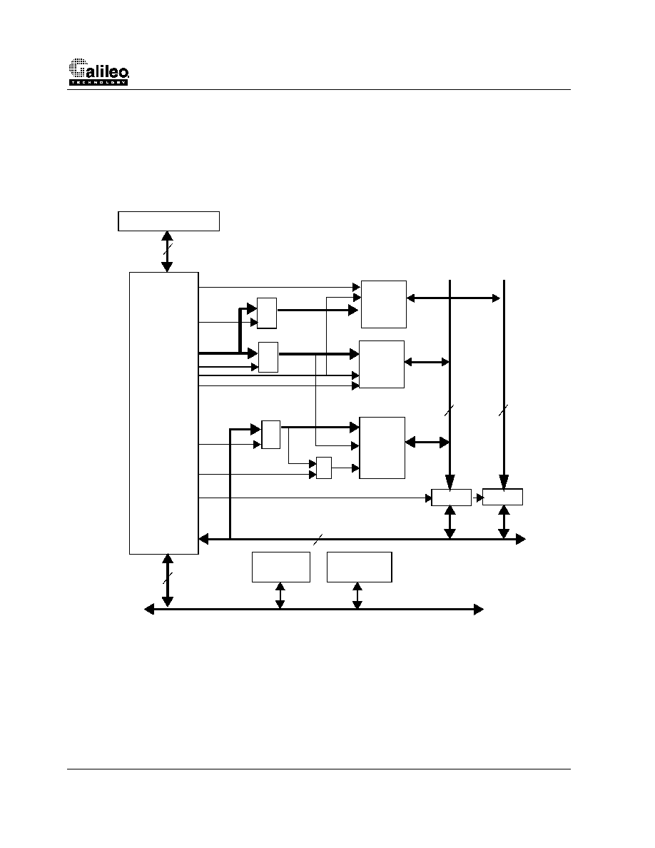
GT-64111 System Controller for RC4640, RM523X and VR4300 CPUs
78
Revision 1.0
15.2
Typical System
The high performance system shown below includes 64-bit wide memories and 32-bit I/O devices on the PCI bus. The
system includes Flash for storing code and data, and DRAM as main memory. In this system data can be moved via
DMA or PCI master accesses between the PCI bus and the Flash or DRAM at full bus bandwidth, at 200 Mbytes per
second. The CPU/Local Master can read from the DRAM at peak bandwidth of 264Mbytes per second. CPU/Local
Master writes have peak bandwidth of 264Mbytes per second for all devices through the GT-64111 on-chip write buffer.
PCI SLAVE
PCI MASTER
DRAM
FLASH
373
373
501
PCI
AD[31:0]
GT-64111
SysAD[31:0]
OR
DAdr[11:0]
LEAdrE
ECAS[3:0]*
ED[31:0]
OD[31:0]
DAdr[2:0]
dev_adr[21:2]
AD[31:0]
ALE
CSTiming*
LEE, OEE*, OEB
D[31:0]
BootCS*
CS*
32
32
32
32
501
32
LEO, OEO*,
OEB
DAdr[11:0]
373
LEAdr0
DRAM
OCAS[3:0]*
RAS*
RAS*
MIPS CPU

GT-64111 System Controller for RC4640, RM523X and VR4300 CPUs
Revision 1.0
15.3
Interface to Asynchronous Devices
In this case, we show the connectivity between the GT-64111 and 64 bit-wide standard memory devices (e.g. SRAM).
In this example the latches selected are industry standard FCT16501 for data, FCT16373 for the address, and
FCT16373 for the burst address for the odd bank. The data latches that interface to the AD bus are used to interleave
the data in read and write access from the GT-64111 and enable data rate of one data per cycle at 66MHz (200 Mbytes
per second peak rate). FCT16373 logic chips are used to latch the address, the CS* and the DevRW*for the Devices.
The latch for the odd bank burst address is needed for the address interleaving. This system configuration is for little
endian, no decrement.
LEE
OEE*
ALE
LEO
OEO*
CS[0]*
CS[0]*
AD[31:0]
OEB
OEB
EWr[3:0]*
OWr[3:0]*
DAdr[2:1]
BAdr[2:1]
DevOE*
FLASH
EPROM
SRAM
ROM
FLASH
EPROM
SRAM
373
Odd Bank
Even Bank
ROM
373
LEAdrO
GT-
DevOE*
OR
CSTiming*
DevRW*
64111
dev_adr[21:0]
DAdr[2:0]
dev_adr[21:0]
OEAB
LEAB
LEBA
OEBA
*
501
B
A
OEAB
LEAB
LEBA
OEBA
*
501
B
A
32
32
OR
32
32
MIPS CPU

GT-64111 System Controller for RC4640, RM523X and VR4300 CPUs
80
Revision 1.0
15.4
Interface to DRAM
The DRAM and the device interface in a typical system share the same data latches and address latches. In this exam-
ple the DRAM is 64 -bit wide and the even and odd banks share the same RAS[0]* pin. Address for the odd bank is
driven from an FCT16373 latch which is controlled by LEAdrO. The data latches used in this example are FCT16501 to
the AD bus. This system configuration is for little endian, no decrement.
LEAdrO
ECAS[3:0]*
OCAS[3:0]*
DWr*
DWr*
DAdr[11:0]
RAS[0]*
RAS[0]*
Odd Bank
Even Bank
LEE
OEE*
LEO
OEO*
OEB
OEB
373
AD[31:0]
GT-
DRAM
DRAM
64111
OEAB
LEAB
LEBA
OEBA
*
501
B
A
OEAB
LEAB
LEBA
OEBA
*
501
B
A
32
32
32
32
MIPS CPU
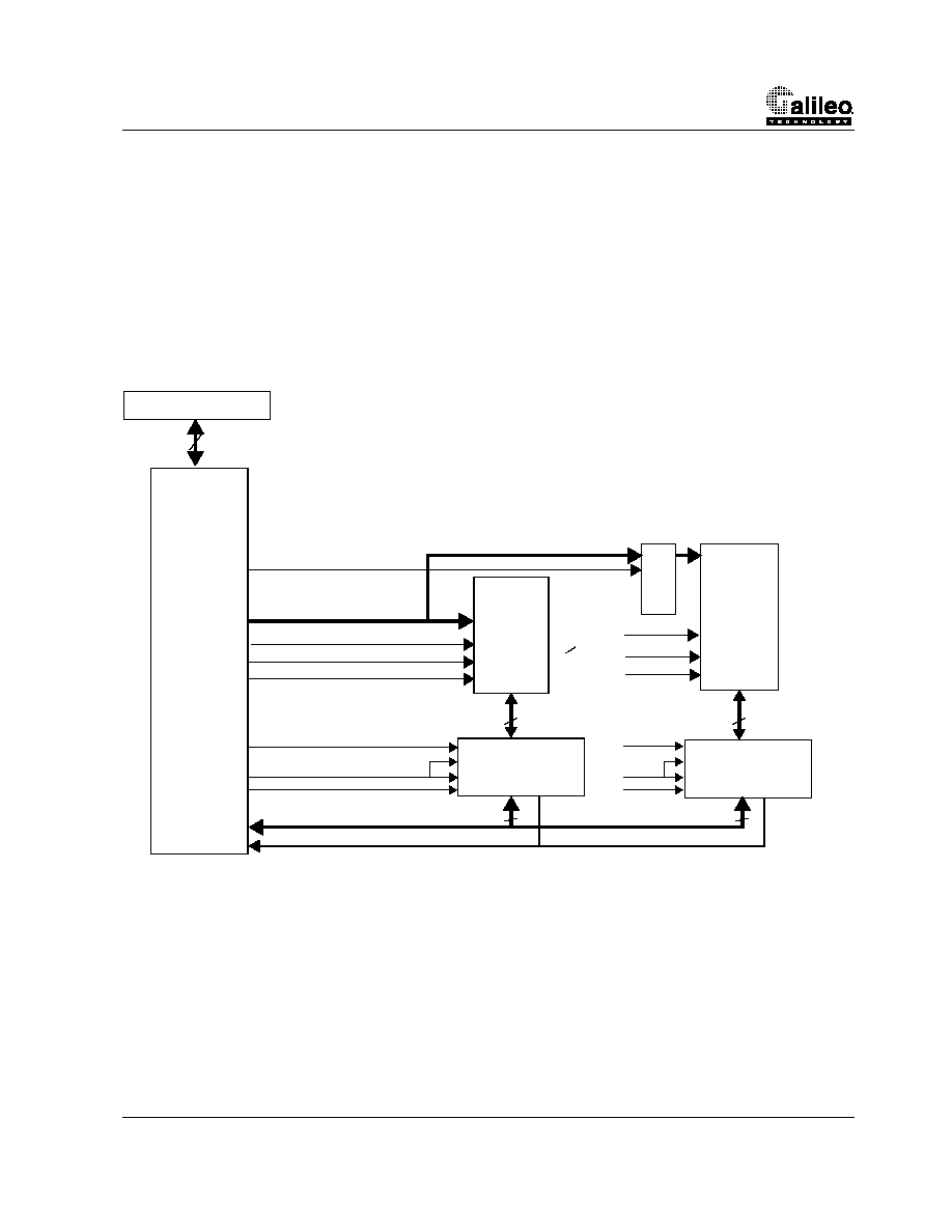
GT-64111 System Controller for RC4640, RM523X and VR4300 CPUs
Revision 1.0
15.5
A System With Parity
In this case, the FCT16511 is used to generate parity for all the write accesses to the devices and the DRAM. In a CPU/
Local Master read access the FCT16511 will check parity and will assert the ParErr* signal when an error is detected.
The GT-64111 will indicate to the CPU/Local Master that the returned data is erroneous via SysCmd[5] and will inter-
rupt the CPU/Local Master if the bank that the CPU/Local Master read from was programmed to have parity integrity
checks. The GT-64111 also asserts SysCmd[4] to indicate to the CPU/Local Master if the read access was from an
address with parity integrity so that the CPU/Local Master will check parity internally as well. In PCI read accesses, an
active ParErr* to a bank that has parity integrity, will cause an assertion of PErr* on the PCI. Notice that with the
FCT16511 the OEAB* polarity is active low, as opposed to the FCT16501, and thus OEB from the GT-64111 should be
programmed accordingly at reset. This system configuration is for little endian, no decrement.
LEAdrO
ECAS[3:0]*
OCAS[3:0]*
DWr*
DWr*
DAdr[11:0]
RAS[0]*
RAS[0]*
Odd Bank
Even Bank
LEE
OEE*
LEO
OEO*
OEB
OEB
OEAB*
LEAB
LEBA
OEBA
*
B
A
841
AD[31:0]
GT-
511
ParErr*
PERA*
32
32
36
36
32
64111
DRAM
DRAM
OEAB*
LEAB
LEBA
OEBA
*
B
A
511
PERA*
36
MIPS CPU

GT-64111 System Controller for RC4640, RM523X and VR4300 CPUs
82
Revision 1.0

GT-64111 System Controller for RC4640, RM523X and VR4300 CPUs
Revision 1.0
16.
Designing for Compatibility with the GT-64011
The GT-64111 is nearly drop-in compatible with the GT-64011 device. With careful hardware and software design it is
possible to design a system that can accept both devices. This section highlights the differences between the two
chips, and explains how to design to handle these differences.
16.1
Major Hardware Differences Between the GT-64011 and GT-64111
The only major differences between the two devices are:
∑
The GT-64111 requires a Vcc of 3.3V; the GT-64011 is a 5V part. You will need to design your board to
deliver the proper voltage to the supply plane depending on which device is installed. Zero-ohm resistors are a
good way to do this.
∑
The Vref pin on the GT-64011 is replaced by Vio on the GT-64111. The GT-64011 used Vref to set the CPU
interface voltage to either 3.3V or 5V depending on the voltage sampled on the pin. The GT-64111 uses this
pin to set the PCI voltage to either 3.3V or 5V; the CPU interface voltage is always 3.3V on the GT-64111. Your
system may need a jumper or zero-ohm resistor to account for this change.
∑
Pin 15 is a Vss on the GT-64011; it is 66MHz PCI Comaptible Enable on the GT-64111. If your system
does not need the 66MHz Compatibility bit set then tie this to Vss directly. If you need to be able to upgrade
from a GT-64011 and want to be able to advertise (in configration space) 66MHz capability, then tie this pin to
a jumper that can be Vss or Vcc. In any case, the PCI bus will still run at 66MHz.
16.2
All Differences Between the GT-64011 and GT-64111
Table 29, below, outlines all differences between the GT-64011 and GT-64111 and include comments on their potential
system implications.
TABLE 29. Differences Between the GT-64011 and GT-64111
F u n c t i o n
G T - 6 4 0 11
G T - 6 4 111
C o m m e n t o n C o m p a t i b i l i t y
Vcc
5V
3.3V
Board must have the capability of supplying
either 5V or 3.3V to Vcc.
Pin 80
Vref
Vio
You may need a jumper to connect this pin
to Vref for GT-64011 designs; Vio for GT-
64111 designs.
Pin 15
Vss
66MHz Capabil-
ity Enable
You may need a jumper to enable the
"advertisement" of 66MHz capability in the
PCI header (see above). This pin does not
affect the actual speed of the PCI interface.
PCI Bus Frequency
33MHz
66MHz
No issues other than the 66MHz Capability
bit.
4300 Bus Mode Sup-
port
None
Yes
ValidOut* pulled-up to Vdd through a
4.7KOhm resistor.
Linear Burst Address
Support
None
Enabled
through bit 9 of
register 0x454
There should be no issues as long as your
software does not set reserved bit in regis-
ters (especially 0x454).
Default Class Code
0x0600
0x0580
There may be issues with drivers written for
class code 0x0600. The class code in the
GT-64111 can be overwritten by software if
this is the case.
RevID
0x01
0x10
There should be no issues as long as your
software/drivers account for the fact that
RevIDs change with silicon stepping.

GT-64111 System Controller for RC4640, RM523X and VR4300 CPUs
84
Revision 1.0
Base Address
Enable Register
RESET state
Enabled
Most disabled
Your software may need to manually
enable the less often used BARs that are
now disabled by default. (This change was
made for PC add-in cards without boot
ROMs.)
Prefetch bit in Mem-
ory BARs
Read/Write
Hardwired to "1"
No issues.
Errata fixes
All known errata
corrected.
Please check your GT-64011 for
workarounds that may no longer be neces-
sary.
F u n c t i o n
G T - 6 4 0 11
G T - 6 4 111
C o m m e n t o n C o m p a t i b i l i t y
GT-64111 System Controller for RC4640, RM523X and VR4300 CPUs
Revision 1.0
17.
REGISTER TABLES
The GT-64111's internal registers can be accessed by the CPU/Local Master or from the PCI bus. They are memory-
mapped for the CPU/Local Master and memory- or I/O-mapped for the PCI. The registers' address is comprised of the
value in the "Internal Space Decode" register and the register offset. The value in the "Internal Space Decode" register
[10:0] is matched against bits [31:21] of the actual address; therefore, this value should be the actual address bits
[31:21] shifted right once.
For example, to access "Channel 0 DMA Byte Count" register (offset 0x800) immediately after Reset*, the full address
will be the default value in the "Internal Space Decode" register which is 0x0a0 shifted left once, which gives 0x140,
two zero's and the offset 0x800, to become a 32-bit address of 0x14000800. The location of the registers in the mem-
ory space can be changed by changing the value programmed into the "Internal Space Decode" register. For example
after changing the value in the "Internal Space Decode" register by writing to 0x14000068 a value of "0bd", an access
to the "Channel 0 DMA Byte Count" register will be with 0x17a00800.
Detailed information about setting the registers is contained in their respective sections of this data sheet.
17.1
Access to On-Chip PCI Configuration Space Registers
An access to a PCI configuration register is performed differently than accesses to all other registers. The access is
performed indirectly by writing the PCI configuration register offset into the Configuration Address register and then
reading or writing the data from/to the Configuration Data register.
For example, to read data from the Status and Command register, the register offset "0x004" is written into the Config-
uration Address register, offset 0xcf8 (or full address from the previous example 0xbd000cf8). Then, reading from the
Configuration Data register (offset 0xcfc), will return the data of the Status and Command register.
17.2
Register Map
Description
Offset
CPU/Local Master Interface
CPU/Local Master Interface Configuration
0x000
Processor Address Space
RAS[1:0] Low Decode Address
0x008
RAS[1:0] High Decode Address
0x010
RAS[3:2] Low Decode Address
0x018
RAS[3:2] High Decode Address
0x020
CS[2:0] Low Decode Address
0x028
CS[2:0] High Decode Address
0x030
CS[3] & Boot CS Low Decode Address
0x038
CS[3] & Boot CS High Decode Address
0x040
PCI I/O Low Decode Address
0x048
PCI I/O High Decode Address
0x050
PCI Memory 0 Low Decode Address
0x058
PCI Memory 0 High Decode Address
0x060
Internal Space Decode
0x068

GT-64111 System Controller for RC4640, RM523X and VR4300 CPUs
86
Revision 1.0
Bus Error Address Low Processor
0x070
Read Only `0'
0x078
PCI Memory 1 Low Decode Address
0x080
PCI Memory 1 High Decode Address
0x088
DRAM and Device Address Space
RAS[0] Low Decode Address
0x400
RAS[0] High Decode Address
0x404
RAS[1] Low Decode Address
0x408
RAS[1] High Decode Address
0x40c
RAS[2] Low Decode Address
0x410
RAS[2] High Decode Address
0x414
RAS[3] Low Decode Address
0x418
RAS[3] High Decode Address
0x41c
CS[0] Low Decode Address
0x420
CS[0] High Decode Address
0x424
CS[1] Low Decode Address
0x428
CS[1] High Decode Address
0x42c
CS[2] Low Decode Address
0x430
CS[2] High Decode Address
0x434
CS[3] Low Decode Address
0x438
CS[3] High Decode Address
0x43c
Boot CS Low Decode Address
0x440
Boot CS High Decode Address
0x444
Address Decode Error
0x470
DRAM Configuration
DRAM Configuration
0x448
DRAM Parameters
DRAM Bank0 Parameters
0x44c
DRAM Bank1 Parameters
0x450
DRAM Bank2 Parameters
0x454
DRAM Bank3 Parameters
0x458
Device Parameters
GT-64111 System Controller for RC4640, RM523X and VR4300 CPUs
Revision 1.0
Device Bank0 Parameters
0x45c
Device Bank1 Parameters
0x460
Device Bank2 Parameters
0x464
Device Bank3 Parameters
0x468
Device Boot Bank Parameters
0x46c
DMA Record
Channel 0 DMA Byte Count
0x800
Channel 1 DMA Byte Count
0x804
Channel 2 DMA Byte Count
0x808
Channel 3 DMA Byte Count
0x80c
Channel 0 DMA Source Address
0x810
Channel 1 DMA Source Address
0x814
Channel 2 DMA Source Address
0x818
Channel 3 DMA Source Address
0x81c
Channel 0 DMA Destination Address
0x820
Channel 1 DMA Destination Address
0x824
Channel 2 DMA Destination Address
0x828
Channel 3 DMA Destination Address
0x82c
Channel 0 Next Record Pointer
0x830
Channel 1 Next Record Pointer
0x834
Channel 2 Next Record Pointer
0x838
Channel 3 Next Record Pointer
0x83c
DMA Channel Control
Channel 0 Control
0x840
Channel 1 Control
0x844
Channel 2 Control
0x848
Channel 3 Control
0x84c
DMA Arbiter
Arbiter Control
0x860
Timer/Counter
Timer /Counter 0
0x850
Timer /Counter 1
0x854
Timer /Counter 2
0x858

GT-64111 System Controller for RC4640, RM523X and VR4300 CPUs
88
Revision 1.0
Timer /Counter 3
0x85c
Timer /Counter Control
0x864
PCI Internal
Command
0xc00
Time Out & Retry
0xc04
RAS[1:0] Bank Size
0xc08
RAS[3:2] Bank Size
0xc0c
CS[2:0] Bank Size
0xc10
CS[3] & Boot CS Bank Size
0xc14
SErr Mask
0xc28
Interrupt Acknowledge
0xc34
Base Address Registers' Enable
0xc3c
Configuration Address
0xcf8
Configuration
Data 0xcfc
Interrupts
Interrupt Cause
0xc18
CPU/Local Master Mask
0xc1c
PCI Mask
0xc24
PCI Configuration
Device and Vendor ID
0x000
Status and Command
0x004
Class Code and Revision ID
0x008
BIST, Header Type, Latency Timer, Cache Line
0x00c
RAS[1:0] Base Address
0x010
RAS[3:2] Base Address
0x014
Subsystem Device and Vendor ID
0x02c
CS[2:0] Base Address
0x018
CS[3] & Boot CS Base Address
0x01c
Internal Registers Memory Mapped Base Address
0x020
Internal Registers I/O Mapped Base Address
0x024
Expansion ROM Base Address Register
0x030
Interrupt Pin and Line
0x03c
PCI Configuration, Function 1

GT-64111 System Controller for RC4640, RM523X and VR4300 CPUs
Revision 1.0
RAS[1:0] Swapped Base Address
0x010
CAS[3:2] Swapped Base Address
0x014
CS[3] and Boot CS Swapped Base Address
and Expansion ROM Base
0x01c

GT-64111 System Controller for RC4640, RM523X and VR4300 CPUs
90
Revision 1.0
17.3
CPU/Local Master Interface
CPU/Local Master Interface Configuration, Offset: 0x000
17.4
CPU/Local Master Decode
RAS[1:0] Low Decode Address, Offset: 0x008
RAS[1:0] High Decode Address, Offset: 0x010
RAS[3:2] Low Decode Address, Offset: 0x018
RAS[3:2] High Decode Address, Offset: 0x020
Bits
Field name
Function
Initial Value
10:0
Reserved
Read Only `0'.
0x0
11
WriteMode
Write mode.
0 - Pipelined writes mode
1 - R4000 mode (2 dead-cycles minimum between
consecutive address-phases)
0x0
12
Endianess
Byte Orientation.
0 - Big Endian
1 - Little Endian
Sampled at Rst* via
the Interrupt* pin
31:13
Reserved
0x0
Bits
Field Name
Function
Initial Value
10:0
Low
DRAM banks 1 and 0 will be accessed when the
decoded addresses are between Low and High.
0x000
31:11
Reserved
0x0
Bits
Field Name
Function
Initial Value
6:0
High
DRAM banks 1 and 0 will be accessed when the
decoded addresses are between Low and High.
0x07
31:7
Reserved
0x0
Bits
Field Name
Function
Initial Value
10:0
Low
DRAM banks 3 and 2 will be accessed when the
decoded addresses are between Low and High.
0x008
31:11
Reserved
0x0
Bits
Field Name
Function
Initial Value
6:0
High
DRAM banks 3 and 2 will be accessed when the
decoded addresses are between Low and High.
0x0f
31:7
Reserved
0x0

GT-64111 System Controller for RC4640, RM523X and VR4300 CPUs
Revision 1.0
CS[2:0] Low Decode Address, Offset: 0x028
CS[2:0] High Decode Address, Offset: 0x030
CS[3] & Boot CS Low Decode Address, Offset: 0x038
CS[3] & Boot CS High Decode Address, Offset: 0x040
PCI I/O Low Decode Address, Offset: 0x048
PCI I/O High Decode Address, Offset: 0x050
Bits
Field Name
Function
Initial Value
10:0
Low
Device banks 2, 1 and 0 will be accessed when the
decoded addresses are between Low and High.
0x0e0
31:11
Reserved
0x0
Bits
Field Name
Function
Initial Value
6:0
High
Device banks 2, 1 and 0 will be accessed when the
decoded addresses are between Low and High.
0x70
31:7
Reserved
0x0
Bits
Field Name
Function
Initial Value
10:0
Low
Device bank 3 and the boot bank will be accessed
when the decoded addresses are between Low and
High.
0x0f8
31:11
Reserved
0x0
Bits
Field Name
Function
Initial Value
6:0
High
Device bank 3 and the boot bank will be accessed
when the decoded addresses are between Low and
High.
0x7f
31:7
Reserved
0x0
Bits
Field Name
Function
Initial Value
10:0
Low
The PCI I/O address space will be accessed when the
decoded addresses are between Low and High.
0x080
31:11
Reserved
0x0
Bits
Field Name
Function
Initial Value
6:0
High
The PCI I/O address space will be accessed when the
decoded addresses are between Low and High.
0x0f
31:7
Reserved
0x0

GT-64111 System Controller for RC4640, RM523X and VR4300 CPUs
92
Revision 1.0
PCI Memory 0 Low Decode Address, Offset: 0x058
PCI Memory 0 High Decode Address, Offset: 0x060
Internal Space Decode, Offset: 0x068
Bus Error Address Processor, Offset: 0x070
Reserved, Offset: 0x078
PCI Memory 1 Low Decode Address, Offset: 0x080
Bits
Field Name
Function
Initial Value
10:0
Low
The PCI memory 0 address space will be accessed
when the decoded addresses are between Low and
High.
0x090
31:11
Reserved
0x0
Bits
Field Name
Function
Initial Value
6:0
High
The PCI memory 0 address space will be accessed
when the decoded addresses are between Low and
High.
0x1f
31:7
Reserved
0x0
Bits
Field Name
Function
Initial Value
10:0
IntDecode
Registers inside the GT-64111 will be accessed when
MasAD bits 31:21 match the value programmed in
bits 10:0.
0x0a0
31:11
Reserved
0x0
Bits
Field Name
Function
Initial Value
31:0
IlegLoAdd
This register captures bits 31:0 of an illegal 32-bit
address.
0x00000000
Bits
Field Name
Function
Initial Value
31:0
Reserved
Read Only `0'.
0x0
Bits
Field Name
Function
Initial Value
10:0
Low
The PCI memory address space will be accessed
when the decoded addresses are between Low and
High.
0x790
31:11
Reserved
0x0
GT-64111 System Controller for RC4640, RM523X and VR4300 CPUs
Revision 1.0
PCI Memory 1 High Decode Address, Offset: 0x088
17.5
Device Decode
RAS[0] Low Decode Address, Offset: 0x400
RAS[0] High Decode Address, Offset: 0x404
RAS[1] Low Decode Address, Offset: 0x408
RAS[1] High Decode Address, Offset: 0x40c
RAS[2] Low Decode Address, Offset: 0x410
Bits
Field Name
Function
Initial Value
6:0
High
The PCI memory address space will be accessed
when the decoded addresses are between Low and
High.
0x1f
31:7
Reserved
0x0
Bits
Field Name
Function
Initial Value
7:0
Low
DRAM bank 0 will be accessed when the decoded
addresses are between Low and High.
0x00
31:8
Reserved
0x0
Bits
Field Name
Function
Initial Value
7:0
High
DRAM bank 0 will be accessed when the decoded
addresses are between Low and High.
0x07
31:8
Reserved
0x0
Bits
Field Name
Function
Initial Value
7:0
Low
DRAM bank 1 will be accessed when the decoded
addresses are between Low and High.
0x08
31:8
Reserved
0x0
Bits
Field Name
Function
Initial Value
7:0
High
DRAM bank 1 will be accessed when the decoded
addresses are between Low and High.
0x0f
31:8
Reserved
0x0
Bits
Field Name
Function
Initial Value
7:0
Low
DRAM bank 2 will be accessed when the decoded
addresses are between Low and High.
0x10
31:8
Reserved
0x0

GT-64111 System Controller for RC4640, RM523X and VR4300 CPUs
94
Revision 1.0
RAS[2] High Decode Address, Offset: 0x414
RAS[3] Low Decode Address, Offset: 0x418
RAS[3] High Decode Address, Offset: 0x41c
CS[0] Low Decode Address, Offset: 0x420
CS[0] High Decode Address, Offset: 0x424
CS[1] Low Decode Address, Offset: 0x428
Bits
Field Name
Function
Initial Value
7:0
High
DRAM bank 2 will be accessed when the decoded
addresses are between Low and High.
0x17
31:8
Reserved
0x0
Bits
Field Name
Function
Initial Value
7:0
Low
DRAM bank 3 will be accessed when the decoded
addresses are between Low and High.
0x18
31:8
Reserved
0x0
Bits
Field Name
Function
Initial Value
7:0
High
DRAM bank 3 will be accessed when the decoded
addresses are between Low and High.
0x1f
31:8
Reserved
0x0
Bits
Field Name
Function
Initial Value
7:0
Low
Device bank 0 will be accessed when the decoded
addresses are between Low and High.
0xc0
31:8
Reserved
0x0
Bits
Field Name
Function
Initial Value
7:0
High
Device bank 0 will be accessed when the decoded
addresses are between Low and High.
0xc7
31:8
Reserved
0x0
Bits
Field Name
Function
Initial Value
7:0
Low
Device bank 1 will be accessed when the decoded
addresses are between Low and High.
0xc8
31:8
Reserved
0x0

GT-64111 System Controller for RC4640, RM523X and VR4300 CPUs
Revision 1.0
CS[1] High Decode Address, Offset: 0x42c
CS[2] Low Decode Address, Offset: 0x430
CS[2] High Decode Address, Offset: 0x434
CS[3] Low Decode Address, Offset: 0x438
CS[3] High Decode Address, Offset: 0x43c
Boot CS Low Decode Address, Offset: 0x440
Bits
Field Name
Function
Initial Value
7:0
High
Device bank 1 will be accessed when the decoded
addresses are between Low and High.
0xcf
31:8
Reserved
0x0
Bits
Field Name
Function
Initial Value
7:0
Low
Device bank 2 will be accessed when the decoded
addresses are between Low and High.
0xd0
31:8
Reserved
0x0
Bits
Field Name
Function
Initial Value
7:0
High
Device bank 2 will be accessed when the decoded
addresses are between Low and High.
0xdf
31:8
Reserved
0x0
Bits
Field Name
Function
Initial Value
7:0
Low
Device bank 3 will be accessed when the decoded
addresses are between Low and High.
0xf0
31:8
Reserved
0x0
Bits
Field Name
Function
Initial Value
7:0
High
Device bank 3 will be accessed when the decoded
addresses are between Low and High.
0xfb
31:8
Reserved
0x0
Bits
Field Name
Function
Initial Value
7:0
Low
Boot bank will be accessed when the decoded
addresses are between Low and High.
0xfc
31:8
Reserved
0x0

GT-64111 System Controller for RC4640, RM523X and VR4300 CPUs
96
Revision 1.0
Boot CS High Decode Address, Offset: 0x444
Address Decode Error, Offset: 0x470
17.6
DRAM Configuration
DRAM Configuration, Offset: 0x448
17.7
DRAM Parameters
DRAM Bank0 Parameters, Offset: 0x44c
Bits
Field Name
Function
Initial Value
7:0
High
Boot bank will be accessed when the decoded
addresses are between Low and High.
0xff
31:8
Reserved
0x0
Bits
Field Name
Function
Initial Value
31:0
ErrAddr
The addresses of accesses to invalid address ranges
(those not in the range programmed in the DRAM or
device decode registers) will be captured in this regis-
ter.
Undefined Value
Bits
Field name
Function
Initial Value
13:0
RefIntCnt
Refresh interval count value.
0x0200
15:14
Reserved
When written, this bits can be safely programmed
to any value. When read, these bits will respond with
an undefined value.
N/A
16
StagRef
Staggered refresh.
0 - Staggered refresh
1- All banks are refreshed together
0x0
17
ADSFunct
Defines the function of the DAdr[11]/ADS* pin.
0 - DAdr11 only
1 - ADS* only
0x0
18
DRAMLatch
Sets the latch operation mode.
0 -The latch control signals are active.
1 - The external data latches are transparent in DRAM
accesses when CAS is programmed to be one cycle
long
0x0
31:19
Reserved
When written, these bits can be safely programmed
to any value. When read, these bits will respond with
an undefined value.
N/A
Bits
Field name
Function
Initial Value
0
CASWr
The number of cycles CAS* is LOW in a write access.
0 - One cycle
1 - Two cycles
0x1
1
RAStoCASWr
The number of cycles between RAS* going active and
CAS* going active in a write access.
0 - Two cycles
1 - Three cycles
0x1

GT-64111 System Controller for RC4640, RM523X and VR4300 CPUs
Revision 1.0
DRAM Bank1 Parameters, Offset: 0x450
DRAM Bank2 Parameters, Offset: 0x454
DRAM Bank3 Parameters, Offset: 0x458
2
CASRd
The number of cycles CAS* is LOW in a read access.
0 - One cycle
1 - Two cycles
0x1
3
RAStoCASRd
The number of cycles between RAS* going active and
CAS* going active in a read access.
0 - Two cycles
1 - Three cycles
0x1
5:4
Refresh
DRAM type support.
00 - 1/2K Refresh (9 bits row, 9 to 12 bits column)
01 - 1K Refresh (10 bits row, 9 to 12 bits column)
10 - 2K Refresh (11 bits row, 9 to 12 bits column)
11 - 4K Refresh (12 bits row, 9 to 12 bits column)
0x0
6
BankWidth
Width of DRAM bank.
0- 32 (36) bit wide DRAM
1- 64 (72) bit wide interleaved DRAM
0x0
7
BankLoc
Location of a 32-bit wide bank.
0- Even
1- Odd
0x0
8
Parity
Parity support for the bank.
0- No parity support
1- Parity supported
0x0
9
Reserved
Must be Programmed `0'.
0x0
31:10
Reserved
When written, these bits can be safely programmed
to any value. When read, these bits will respond with
an undefined value.
N/A
Bits
Field Name
Function
Initial Value
31:0
Various
Fields function as in DRAM Bank0.
0xf
Bits
Field Name
Function
Initial Value
0:8
Various
Fields function as in DRAM Bank0.
0xf
9
LinearBurst
Sub-block order or linear burst order DRAM select.
0 - Sub-block order
1 - Linear Burst order
0x0
31:10
Various
Fields function as in DRAM Bank0.
0x0
Bits
Field Name
Function
Initial Value
31:0
Various
Fields function as in DRAM Bank0.
0xf
Bits
Field name
Function
Initial Value

GT-64111 System Controller for RC4640, RM523X and VR4300 CPUs
98
Revision 1.0
17.8
Device Parameters
Device Bank0 Parameters, Offset: 0x45c
Bits
Field name
Function
Initial Value
2:0
TurnOff
The number of cycles between the deassertion of
DevOE* (an externally extracted signal which is the
logical OR between CSTiming* and inverted DevRW*)
to a new AD bus cycle.
0x7
6:3
AccToFirst
The number of cycles in a read access from the
assertion of CS* to the cycle that the data will be
latched (by the external latches). Can be extended via
the Ready* pin.
0xf
10:7
AccToNext
The number of cycles in a read access from the cycle
that the first data was latched to the cycle that the
next data will be latched (in burst accesses). Can be
extended via the Ready* pin.
0xf
13:11
ADStoWr
The number of cycles from ADS* active to the asser-
tion of EWr* or OWr*.
0x7
16:14
WrActive
The number of cycles EWr* or OWr* are active. Can
be extended via the Ready* pin.
0x7
19:17
WrHigh
The number of cycles between deassertion and
assertion of EWr* or OWr*.
0x7
21:20
DevWidth
Device width.
00 - 8 bits
01 - 16 bits
10 - 32 bits
11 - 64 bits
0x2
22
Reserved
Must be programmed `1'.
0x1
23
DevLoc
32-bit, 16-bit, or 8-bit device location.
0 - Even bank
1 - Odd bank
0x0
24 Reserved
Read
only.
0x0
25
LatchFunct
Latch function in read cycles.
0 - Always transparent
1 - Latch enable signals are active.
0x0
27:26
Reserved
Read only.
0x1
29:28
Reserved
Read only.
0x1
30
Parity
Parity support for the bank.
0- No parity support
1- Parity supported
0x0
31
Reserved
When written, this bit can be safely programmed
to any value. When read, this bit will respond with
an undefined value.
N/A

GT-64111 System Controller for RC4640, RM523X and VR4300 CPUs
Revision 1.0
Device Bank1 Parameters, Offset: 0x460
Device Bank2 Parameters, Offset: 0x464
Device Bank3 Parameters, Offset: 0x468
Device Boot Bank Parameters, Offset: 0x46c
In case of the CS[3]* or Boot Bank, bits 23:20 are shown as `?' because bits 21:20 are sampled at reset via DAdr[11:10]
to define the width of the device.
17.9
DMA Record
Channel 0 DMA Byte Count, Offset: 0x800
Channel 1 DMA Byte Count, Offset: 0x804
Channel 2 DMA Byte Count, Offset: 0x808
Bits
Field Name
Function
Initial Value
31:0
Various
Fields function as in Device Bank0.
0x146fffff
Bits
Field Name
Function
Initial Value
31:0
Various
Fields function as in Device Bank0.
0x146fffff
Bits
Field Name
Function
Initial Value
31:0
Various
Fields function as in Device Bank0.
0x14?fffff
Bits
Field Name
Function
Initial Value
31:0
Various
Fields function as in Device Bank0.
0x14?fffff
Bits
Field Name
Function
Initial Value
15:0
ByteCt
The number of bytes that are left in DMA transfers.
0x0
31:16
Reserved
0x0
Bits
Field Name
Function
Initial Value
15:0
ByteCt
The number of bytes that are left in DMA transfers.
0x0
31:16
Reserved
0x0
Bits
Field Name
Function
Initial Value
15:0
ByteCt
The number of bytes that are left in DMA transfers.
0x0
31:16
Reserved
0x0

GT-64111 System Controller for RC4640, RM523X and VR4300 CPUs
100
Revision 1.0
Channel 3 DMA Byte Count, Offset: 0x80c
Channel 0 DMA Source Address, Offset: 0x810
Channel 1 DMA Source Address, Offset: 0x814
Channel 2 DMA Source Address, Offset: 0x818
Channel 3 DMA Source Address, Offset: 0x81c
Channel 0 DMA Destination Address, Offset: 0x820
Channel 1 DMA Destination Address, Offset: 0x824
Bits
Field Name
Function
Initial Value
15:0
ByteCt
The number of bytes that are left in DMA transfers.
0x0
31:16
Reserved
0x0
Bits
Field Name
Function
Initial Value
31:0
SrcAdd
The address that the DMA controller will read the data
from.
0x0
Bits
Field Name
Function
Initial Value
31:0
SrcAdd
The address that the DMA controller will read the data
from.
0x0
Bits
Field Name
Function
Initial Value
31:0
SrcAdd
The address that the DMA controller will read the data
from.
0x0
Bits
Field Name
Function
Initial Value
31:0
SrcAdd
The address that the DMA controller will read the data
from.
0x0
Bits
Field Name
Function
Initial Value
31:0
DestAdd
The address that the DMA controller will write the data
to.
0x0
Bits
Field Name
Function
Initial Value
31:0
DestAdd
The address that the DMA controller will write the data
to.
0x0
GT-64111 System Controller for RC4640, RM523X and VR4300 CPUs
Revision 1.0
Channel 2 DMA Destination Address, Offset: 0x828
Channel 3 DMA Destination Address, Offset: 0x82c
Channel 0 Next Record Pointer, Offset: 0x830
Channel 1 Next Record Pointer, Offset: 0x834
Channel 2 Next Record Pointer, Offset: 0x838
Channel 3 Next Record Pointer, Offset: 0x83c
Bits
Field Name
Function
Initial Value
31:0
DestAdd
The address that the DMA controller will write the data
to.
0x0
Bits
Field Name
Function
Initial Value
31:0
DestAdd
The address that the DMA controller will write the data
to.
0x0
Bits
Field Name
Function
Initial Value
31:0
NextRecPtr
The address for the next record of DMA. A value of 0
means a NULL pointer (end of the chained list).
0x0
Bits
Field Name
Function
Initial Value
31:0
NextRecPtr
The address for the next record of DMA. A value of 0
means a NULL pointer (end of the chained list).
0x0
Bits
Field Name
Function
Initial Value
31:0
NextRecPtr
The address for the next record of DMA. A value of 0
means a NULL pointer (end of the chained list).
0x0
Bits
Field Name
Function
Initial Value
31:0
NextRecPtr
The address for the next record of DMA. A value of 0
means a NULL pointer (end of the chained list).
0x0

GT-64111 System Controller for RC4640, RM523X and VR4300 CPUs
102
Revision 1.0
17.10 DMA Channel Control
Channel 0 Control, Offset: 0x840
Bits
Field name
Function
Initial Value
1:0
AddControl
Sets the locations of the source/destination of the
DMA access (64011/14/60 Rev P-1 and later ONLY):
00 - Source and destination are in the local address
space.
01 - Source is in PCI Memory space and destination
in the local address space.
10 - Destination is in PCI Memory space and source
in the local address space.
11 - Source and destination are in PCI Memory
space.
These bits are RESERVED (must be = `00') in the GT-
64011-P-0 and GT-64010A.
0x0
3:2
SrcDir
Source Direction.
00 - Increment source address
01 - Decrement source address
10 - Hold in the same value
0x0
5:4
DestDir
Destination Direction.
00 - Increment destination address
01 - Decrement destination address
10 - Hold in the same value
0x0
8:6
DataTransLim
Data Transfer Limit in each DMA access.
101 - 1 Byte
110 - 2 Bytes
000 - 4 Bytes
001 - 8 Bytes
011 - 16 Bytes
111 - 32 Bytes
0x0
9
ChainMod
Chained Mode.
0 - Chained mode; when a DMA access is terminated,
the parameters of the next DMA access will come
from a record in memory that a NextRecPtr register
points at.
1 - Non-Chained mode; only the values that are pro-
grammed by the CPU/Local Master (or PCI) directly
into the ByteCt, SrcAdd, and DestAdd registers are
used.
0x0
10
IntMode
Interrupt Mode.
0 - Interrupt asserted every time the DMA byte count
reaches terminal count.
1 - Interrupt every NULL pointer (in Chained mode)
0x0
11
TransMod
Transfer Mode.
0 - Demand
1 - Block
0x0
12
ChanEn
Channel Enable.
0 - Disable
1 - Enable
0x0

GT-64111 System Controller for RC4640, RM523X and VR4300 CPUs
Revision 1.0
Channel 1 Control, Offset: 0x844
Channel 2 Control, Offset: 0x848
Channel 3 Control, Offset: 0x84c
13
FetNexRec
Fetch Next Record.
1 - Forces a fetch of the next record (even if the cur-
rent DMA has not ended). This bit is reset after fetch
is completed (meaningful only in Chained mode).
0x0
14
DMAActSt
DMA Activity Status (read only).
0 - Channel is not active
1 - Channel is active
0x0
31:15
Reserved
0x0
Bits
Field Name
Function
Initial Value
31:0
Various
Fields function as in Channel 0 Control.
0x0
Bits
Field Name
Function
Initial Value
31:0
Various
Fields function as in Channel 0 Control.
0x0
Bits
Field Name
Function
Initial Value
31:0
Various
Fields function as in Channel 0 Control.
0x0
Bits
Field name
Function
Initial Value

GT-64111 System Controller for RC4640, RM523X and VR4300 CPUs
104
Revision 1.0
17.11 Arbiter Control, Offset: 0x860
17.12 Timer / Counter
Timer/Counter 0, Offset: 0x850
Timer/Counter 1, Offset: 0x854
Timer/Counter 2, Offset: 0x858
Bits
Field name
Function
Initial Value
1:0
PrioChan1/0
Priority between Channel 0 and Channel 1.
00 - Round Robin
01 - Priority to channel 1 over channel 0
10 - Priority to channel 0 over channel 1
11 - Reserved
0x0
3:2
PrioChan3/2
Priority between Channel 2 and Channel 3.
00 - Round Robin
01 - Priority to channel 3 over 2
10 - Priority to channel 2 over 3
11 - Reserved
0x0
5:4
PrioGrps
Priority between the group of channels 0/1 and the
group of channels 2/3.
00 - Round Robin
01 - Priority to channels 2/3 over 0/1
10 - Priority to channels 0/1 over 2/3
11 - Reserved
0x0
6
PrioOpt
Defines the arbiter behavior for high priority device.
0 - High priority device will relinquish the bus for a
requesting device for one DMA transaction after it was
serviced.
1 - High priority device will be granted as long as it
requests the bus.
0x0
31:7
Reserved
0x0
Bits
Field Name
Function
Initial Value
31:0
TC0Value
The counter or timer initial value.
0x0
Bits
Field Name
Function
Initial Value
23:0
TC1Value
The counter or timer initial value.
0x0
31:24
Reserved
0x0
Bits
Field Name
Function
Initial Value
23:0
TC2Value
The counter or timer initial value.
0x0
31:24
Reserved
0x0

GT-64111 System Controller for RC4640, RM523X and VR4300 CPUs
Revision 1.0
Timer/Counter 3, Offset: 0x85c
Timer/Counter Control, Offset: 0x864
Bits
Field Name
Function
Initial Value
23:0
TC3Value
The counter or timer initial value.
0x0
31:24
Reserved
0x0
Bits
Field name
Function
Initial Value
0
EnTC0
The timer/counter will count only when it is enabled.
0 - Disable
1 - Enable
0x0
1
SelTC0
Timer or counter selection.
0 - Counter
1 - Timer
0x0
2
EnTC1
The timer/counter will count only when it is enabled.
0 - Disable
1 - Enable
0x0
3
SelTC1
Timer or counter selection.
0 - Counter
1 - Timer
0x0
4
EnTC2
The timer/counter will count only when it is enabled.
0 - Disable
1 - Enable
0x0
5
SelTC2
Timer or counter selection .
0 - Counter
1 - Timer
0x0
6
EnTC3
The timer/counter will count only when it is enabled.
0 - Disable
1 - Enable
0x0
7
SelTC3
Timer or counter selection.
0 - Counter
1 - Timer
0x0
31:8
Reserved
0x0

GT-64111 System Controller for RC4640, RM523X and VR4300 CPUs
106
Revision 1.0
17.13 PCI Internal
Command, Offset: 0xc00
Time Out & ReTry, Offset: 0xc04
1. Regardless of the selected sync mode, PClk frequency must be smaller than Tclk frequency by at least 1MHz
Bits
Field name
Function
Initial Value
0
ByteSwap
When set to zero, the GT-64111 swaps the incoming
and outgoing PCI data.
If there is a PCI Address hit in an enabled SWAP
BAR, the data will be transferred OPPOSITE as it
would according to the setting of ByteSwap.
Set to the same value
sampled at reset into
bit[12] of the CPU/
Local Master Interface
Configuration register.
2:1
SyncMode
1
Indicates the ratio between TClk and PClk as follows:
00 - When the PClk ranges from DC to 66MHz
(default mode; use following settings for higher perfor-
mance)
01 - When PClk frequency is HIGHER than or EQUAL
to half the TClk frequency (e.g. when TClk is 66MHz,
SyncMode can be set to 01 if the PCI frequency is
HIGHER than or equal to 33MHz).
1x - When the two clocks are synchronized (derived
from the same clock) and PClk frequency is HIGHER
than or EQUAL to half the TCLK frequency(e.g. TClk
= 66MHz, PClk = 33MHz)
0x0
31:3
Reserved
0x0
Bits
Field name
Function
Initial Value
7:0
Timeout0
Specifies in PCI clock units the number of clocks the
GT-64111, as a slave, holds the PCI bus before the
generation of retry termination. Used for the first data
transfer.
0x0f
15:8
Timeout1
Specifies in PCI clock units the number of clocks the
GT-64111, as a slave, holds the PCI bus before the
generation of disconnect termination. Used for data
transfers following the first data.The number of PCI
clock cycles between the last Trdy* rise and the Stop*
falling are n+1, where `n' is the Timeout1 value.
0x07
23:16
RetryCtr
Specifies the number of retries of the GT-64111 Mas-
ter. The GT-64111 generates an interrupt when this
timer expires. A value of 0x00 means "retry forever".
The number in RetryCtr does not include the first
access of the transaction.
0x00
31:24
Reserved
0x0

GT-64111 System Controller for RC4640, RM523X and VR4300 CPUs
Revision 1.0
RAS[1:0] Bank Size, Offset: 0xc08
RAS[3:2] Bank Size, Offset: 0xc0c
CS[2:0] Bank Size, Offset: 0xc10
CS[3] and Boot CS Bank Size, Offset: 0xc14
Bits
Field Name
Function
Initial Value
31:12
BankSize
Specifies the RAS[1:0] address mapping in conjunc-
tion with the RAS[1:0] Base Address register.
Set to `0' indicates that the corresponding bit in the
address and in the base address must be equal in
order to have a hit. Set to `1' indicates that the corre-
sponding bit in the address is a don't-care.
For example, bit 12 set to `1' indicates that the
RAS[1:0] size is 8KBytes (address bits [12:0] are
changeable/don't-care). The set bits in the Bank Size
must be sequential (e.g. 000...001, 000...011,
000...111 are correct values, whereas 000...010 and
000...100 are not).
0x00fff
11:0
Reserved
0x0
Bits
Field Name
Function
Initial Value
31:12
BankSize
Specifies the RAS[3:2] address mapping in conjunc-
tion with the RAS[3:2] Base Address register.
Same description and setting restrictions as outlined
for RAS[1:0] Bank Size, Offset: 0xc08.
0x00fff
11:0
Reserved
0x0
Bits
Field Name
Function
Initial Value
31:12
BankSize
Specifies the CS[2:0] address mapping in conjunction
with the CS[2:0] Base Address register.
Same description and setting restrictions as outlined
for RAS[1:0] Bank Size, Offset: 0xc08.
0x01fff
11:0
Reserved
0x0
Bits
Field Name
Function
Initial Value
31:12
BankSize
Specifies the CS[3] and Boot CS address mapping in
conjunction with the CS[3] and Boot CS Base Address
register.
Same description and setting restrictions as outlined
for RAS[1:0] Bank Size, Offset: 0xc08.
0x00fff
11:0
Reserved
0x0

GT-64111 System Controller for RC4640, RM523X and VR4300 CPUs
108
Revision 1.0
SErr Mask, Offset: 0xc28
Interrupt Acknowledge, Offset: 0xc34
Base Address Registers' Enable, Offset: 0xc3c
Bits
Field Name
Function
Initial Value
0
AddrErr
Mask bit. When set, SErr* is asserted when the GT-
64111 detects a parity error on the address lines.
0x0
1
MasWrErr
Mask bit. When set, SErr* is asserted when the GT-
64111 detects a parity error during a master write
operation.
0x0
2
MasRdErr
Mask bit. When set, SErr* is asserted when the GT-
64111 detects a parity error during a master read
operation.
0x0
3
MemErr
Mask bit. When set, SErr* is asserted when a memory
parity error has been detected (applicable only when
an external parity checking device is used).
0x0
4
MasAbort
Mask bit. When set, SErr* is asserted when the GT-
64111 performs master abort.
0x0
5
TarAbort
Mask bit. When set, SErr* is asserted when the GT-
64111 detects a target abort.
0x0
31:6
Reserved
0x0
Bits
Field Name
Function
Initial Value
31:0
IntAck
The data is meaningless. A CPU/Local Master read
operation to this register causes the GT-64111 to per-
form an Interrupt Acknowledge cycle on the PCI bus.
0x00000000
Bits
Field name
Function
Initial Value
31:9
Reserved
0x0
8
RAS[1:0]En
Controls address matching with RAS[1:0] base/size.
0 - Enable
1 - Disable
0x0
7
RAS[3:2]En
Controls address matching with RAS[3:2] base/size.
0 - Enable
1 - Disable
Sampled at Reset via
DMAReq[0]*/Ready*
6
CS[2:0]En
Controls address matching with CS[2:0] base/size.
0 - Enable
1 - Disable
Sampled at Reset via
DAdr[6]
5
CS[3] & Boot CSEn
Controls address matching with CS[3] & Boot CS
base/size.
0 - Enable
1 - Disable
Sampled at Reset via
DAdr[3]
4
IntMeMEn
Controls address matching with internal registers-
Memory mapped base/size.
0 - Enable
1 - Disable
0x0

GT-64111 System Controller for RC4640, RM523X and VR4300 CPUs
Revision 1.0
The GT-64111 prevents disabling both memory mapped base/size address matching and I/O mapped base/size
address matching at the same time (bits 3 and 4 cannot simultaneously be set to 1).
Configuration Address, Offset: 0xcf8
Configuration Data, Offset: 0xcfc
3
IntIOEn
Controls address matching with internal registers I/O
mapped base/size.
0 - Enable
1 - Disable
0x1
2
SwRAS[1:0]En
Controls address matching with Swapped RAS[1:0]
base/size.
0 - Enable
1 - Disable
0x1
1
SwRAS[3:2]En
Controls address matching with Swapped RAS[3:2]
base/size.
0 - Enable
1 - Disable
0x1
0
SwCS[3] & Boot
CSEn
Controls address matching with Swapped CS[3] &
Boot CS base/size.
0 - Enable
1 - Disable
0x1
Bits
Field Name
Function
Initial Value
7:2
RegNum
Indicates the register number.
0x00
10:8
FunctNum
Indicates the function type.
0x0
15:11
DevNum
Indicates the device number.
0x00
23:16
BusNum
Indicates the bus number.
0x00
31
ConfigEn
When set, an access to the Configuration Data regis-
ter is translated into a Configuration or Special cycle
on the PCI bus.
0x0
Bits
Field Name
Function
Initial Value
31:0
Config
The data is transferred to/from the PCI bus when the
CPU/Local Master accesses this register and the
ConfigEn bit in the Configuration Address register is
set. A CPU/Local Master access to this register
causes the GT-64111 to perform a Configuration or
Special cycle on the PCI bus.
0x000
Bits
Field name
Function
Initial Value

GT-64111 System Controller for RC4640, RM523X and VR4300 CPUs
110
Revision 1.0
17.14 Interrupts
Interrupt Cause, Offset: 0xc18
(all bits are cleared by writing a value of `0' by the CPU/ Local Master or PCI, unless stated otherwise)
Bits
Field Name
Function
Initial Value
0
IntSum
Interrupt summary. Logical OR of all the interrupt bits,
regardless of the Mask registers' values.
0x0 Read only
1
MemOut
Asserts when the CPU/Local Master or PCI accesses
an address out of range in the Device Decoders or a
burst access to 8-/16-bit devices.
0x0
2
DMAOut
Asserts when the DMA accesses an address out of
range.
0x0
3
CPU/Local Master-
Out
Asserts when the CPU/Local Master accesses an
address out of the CPU/Local Master decode.
0x0
4
DMA0Comp
Asserts at completion of DMA Channel 0 transfer.
0x0
5
DMA1Comp
Asserts at completion of DMA Channel 1 transfer.
0x0
6
DMA2Comp
Asserts at completion of DMA Channel 2 transfer.
0x0
7
DMA3Comp
Asserts at completion of DMA Channel 3 transfer.
0x0
8
T0Exp
Asserts when Timer 0 expires.
0x0
9
T1Exp
Asserts when Timer 1 expires.
0x0
10
T2Exp
Asserts when Timer 2 expires.
0x0
11
T3Exp
Asserts when Timer 3 expires.
0x0
12
MasRdErr
Asserts when the GT-64111 detects a parity error dur-
ing a master read operation.
0x0
13
SlvWrErr
Asserts when the GT-64111 detects a parity error dur-
ing a slave write operation.
0x0
14
MasWrErr
Asserts when the GT-64111 detects a parity error dur-
ing a master write operation.
0x0
15
SlvRdErr
Asserts when the GT-64111 detects a parity error dur-
ing a slave read operation.
0x0
16
AddrErr
Asserts when the GT-64111 detects a parity error on
the address lines.
0x0
17
MemErr
Asserts when a memory parity error is detected.
Applicable only when an external parity checking
device is used.
0x0
18
MasAbort
Asserts upon master abort.
0x0
19
TarAbort
Asserts upon target abort.
0x0
20
RetryCtr
Asserts when the retry counter expires.
0x0
25:21
CPU/Local Master-
Int
These bits are set by the CPU/Local Master by writing
`0' to generate an interrupt on the PCI bus. They are
cleared when the PCI writes `0'.
0x0
29:26
PCIInt
These bits are set by the PCI by writing `0' to generate
an interrupt on the CPU/Local Master. They are
cleared when the CPU/Local Master writes `0'.
0x0

GT-64111 System Controller for RC4640, RM523X and VR4300 CPUs
Revision 1.0
CPU/Local Master Mask, Offset: 0xc1c
PCI Mask, Offset: 0xc24
30
CPU/Local Master-
IntSum
Interrupt summary. Logical OR of bits[29:26,20:1],
masked by bits[29:26,20:1] of the CPU/Local Master
Mask register.
0x0
31
PCIIntSum
Interrupt summary. Logical OR of bits[25:1], masked
by bits[25:1] of the PCI Mask register.
0x0
Bits
Field Name
Function
Initial Value
31:0
CPU/Local Master-
Mask
Mask to the CPU/Local Master interrupt line for the
appropriate bits in the Interrupt Cause register. Bits 0,
25:21, 31:30 are read-only "0".
0 - Mask Interrupt
1 - Do not Mask Interrupt
0x00000000
Bits
Field Name
Function
Initial Value
31:0
PCIMask
Mask to the PCI interrupt line for the appropriate bits
in the Interrupt Cause register. Bits 0, 31:26 are read-
only "0".
0 - Mask Interrupt
1 - Do not Mask Interrupt
0x00000000
Bits
Field Name
Function
Initial Value

GT-64111 System Controller for RC4640, RM523X and VR4300 CPUs
112
Revision 1.0
17.15 PCI Configuration Registers
Device and Vendor ID, Offset: 0x000
Status and Command, Offset: 0x004
Bits
Field name
Function
Initial Value
31:16
DevID
Provides the unique GT-64111 ID number (0x146).
0x4146
15:0
VenID
Provides the manufacturer of the GT-64111 (0x11ab).
0x11ab
Bits
Field name
Function
Initial Value
0
IOEn
Controls the GT-64111's response to I/O accesses.
0 - Disable
1 - Enable
0x0
1
MEMEn
Controls the GT-64111's response to Memory
accesses.
0 - Disable
1 - Enable
0x0
2
MasEn
Controls the GT-64111's ability to act as a master on
the PCI bus.
0 - Disable
1 - Enable
0x0
3
Reserved
0x0
4
MemWrInv
Controls the GT-64111's ability to generate Memory
Write & Invalidate command on the PCI bus.
0 - Disable
1 - Enable
0x0
5
Reserved
0x0
6
PErrEn
Controls the GT-64111's ability to respond to parity
errors on the PCI by asserting the PErr* pin.
0 - Disable
1 - Enable
0x0
7
Reserved
0x0
8
SErrEn
Controls the GT-64111's ability to assert the SErr* pin.
0 - Disable
1 - Enable
0x0
21:9
Reserved
0x0
22
66MHzEn
66MHz Capable (GT-64111 PCI interface is capable
of running at 66MHz regardless of this bit value).
Sampled at Reset via
pin 15
23
TarFastBB
Read only bit. Indicates that the GT-64111 is capable
of accepting fast back-to-back transactions on the PCI
bus.
0x1
24
DataParDet
This bit is set by the GT-64111 when it detects a data
parity error during master operation.
0x0
27:25
DevSelTim
These pins indicate the GT-64111 `s DevSel timing
(medium), per the PCI standard.
0x1 Read only
28
TarAbort
This bit is set upon Target Abort.
0x0
29
MasAbort
This pin is set upon Master Abort.
0x0
GT-64111 System Controller for RC4640, RM523X and VR4300 CPUs
Revision 1.0
Class Code and Revision ID, Offset: 0x008
1
BIST, Header Type, Latency Timer, Cache Line, Offset: 0x00c
The BIST Field is reserved and is hardwired to 0.
Device and Vendor ID (0x000), Class Code and Revision ID (0x008), and Header Type (0x00e) fields are ready only
from the PCI bus. These fields can be modified and read via the CPU/Local Master bus.
For more information on these fields, please refer to the PCI specification.
RAS[1:0] Base Address, Offset: 0x010
1. RevID does not start at 0x01 in order to leave "space" for future frevs of the GT-64011
1. The GT-64111 Class Code is different than in the GT-64011. Please see the PCI section for details.
30
SysErr
This pin is set upon System Error.
0x0
31
DetParErr
This pin is set upon detection of Parity error (in both,
master and slave operations).
0x0
Bits
Field name
Function
Initial Value
7:0
RevID
Indicates the GT-64111 Revision number.
GT-64111-P-0 = 0x10
1
0x10
15:8
Reserved
0x0
23:16
SubClass
Indicates the GT-64111 Subclass (0x80 - other mem-
ory controller)
0x80
31:24
BaseClass
Indicates the GT-64111 Base Class (0x5 - memory
controller).
0x05
Bits
Field name
Function
Initial Value
7:0
CacheLine
Specifies the GT-64111's cache line size
0x00
15:8
LatTimer
Specifies in units of PCI bus clocks the value of the
latency timer of the GT-64111.
0x00
23:16
HeadType
Specifies the layout of bytes 10h through 3fh.
0x00
31:24
BIST
Built In Self Test, Reserved
0x00
Bits
Field Name
Function
Initial Value
2:0
Reserved
0x0
3
Prefetch
READ ONLY
0x1
11:4
Reserved
0x0
31:12
Base
Defines the address assignment of RAS[1:0] (see
RAS[1:0] Bank Size
0x00000
Bits
Field name
Function
Initial Value

GT-64111 System Controller for RC4640, RM523X and VR4300 CPUs
114
Revision 1.0
RAS[3:2] Base Address, Offset: 0x014
CS[2:0] Base Address, Offset: 0x018
CS[3] and Boot CS Base Address, Offset: 0x01c
Internal Registers Memory Mapped Base Address, Offset: 0x020
Internal Registers I/O Mapped Base Address, Offset: 0x024
Bits
Field Name
Function
Initial Value
2:0
Reserved
0x0
3
Prefetch
READ ONLY
0x1
11:4
Reserved
0x0
31:12
Base
Defines the address assignment of RAS[3:2] (see
RAS[3:2] Bank Size).
0x01000
Bits
Field Name
Function
Initial Value
2:0
Reserved
0x0
3
Prefetch
READ ONLY
0x1
11:4
Reserved
0x0
31:12
Base
Defines the address assigment of CS[2:0] (see
CS[2:0] Bank Size).
0x1c000
Bits
Field Name
Function
Initial Value
2:0
Reserved
0x0
3
Prefetch
READ ONLY
0x1
11:4
Reserved
0x0
31:12
Base
Defines the address assignment of CS[3] and Boot
CS (see CS[3] and Boot CS Bank Size).
0x1f000
Bits
Field Name
Function
Initial Value
11:0
Reserved
0x0
31:12
MemMapBase
Defines the address assignment of the GT-64111's
internal registers.
0x14000
Bits
Field Name
Function
Initial Value
11:0
Reserved
0x0
31:12
IOMapBase
Defines the address assignment of the GT-64111's
internal registers.
0x14000

GT-64111 System Controller for RC4640, RM523X and VR4300 CPUs
Revision 1.0
Board/System Device and Vendor ID, Offset: 0x02c
Expansion ROM Base Address Register, Offset: 0x030
Interrupt Pin and Line, Offset: 0x03c
17.15.1 FUNCTION 1 CONFIGURATION REGISTERS
These registers can only be accessed by specifying Function 1 during PCI Configuration cycles.
Function 1 RAS[1:0] Swapped Base Address, Offset: 0x010
Bits
Field name
Function
Initial Value
15:0
VenID
Provides the unique Board/System ID number.
0x0
31:16
DevID
Provides the unique Board/System ID number.
0x0
Bits
Field Name
Function
Initial Value
0
ERDecEn
Expansion ROM Decode Enable
0 - Disable
1 - Enable
0x0
11:1
Reserved
0x0
31:12
ERBase
Defines the address of the expansion ROM memory
space region assigned to the GT-64111. This is
where the expansion ROM code will appear in system
memory when bit 0 of this register contains a value of
1 and bit 1 of this device's Command Register con-
tains a value of 1.
0x1f000
Bits
Field name
Function
Initial Value
7:0
IntLine
Provides interrupt line routing information.
0x00
15:8
IntPin
Indicates which interrupt pin is used by the GT-64111.
The GT-64111 uses INTA.
0x01
31:16
Reserved
0x0
Bits
Field Name
Function
Initial Value
2:0
Reserved
0x0
3
Prefetch
READ ONLY
0x1
11:4
Reserved
0x0
31:12
Base
Defines the address assignment of swapped RAS[1:0]
(see RAS[1:0] Bank Size).
0x0000
GT-64111 System Controller for RC4640, RM523X and VR4300 CPUs
116
Revision 1.0
Function 1 RAS[3:2] Swapped Base Address, Offset: 0x014
Function 1 CS[3] and Boot CS Swapped Base Address, Offset: 0x01c
For more information on these fields, please refer to the PCI specification.
Bits
Field Name
Function
Initial Value
2:0
Reserved
0x0
3
Prefetch
READ ONLY
0x1
11:4
Reserved
0x0
31:12
Base
Defines the address assignment of swapped RAS[3:2]
(see RAS[3:2] Bank Size).
0x01000
Bits
Field Name
Function
Initial Value
2:0
Reserved
0x0
3
Prefetch
READ ONLY
0x1
11:4
Reserved
0x0
31:12
Base
Defines the address assignment of swapped CS[3]
and Boot CS (see CS[3] and Boot CS Bank Size).
0x1f000

GT-64111 System Controller for RC4640, RM523X and VR4300 CPUs
Revision 1.0
18.
PINOUT TABLE, 208 pin PQFP (sorted by number)
P i n
#
S i g n a l
N a m e
P i n
#
S i g n a l
N a m e
P i n
#
S i g n a l
Na m e
1
VDD
36
PAD[15]
71
SysCmd[1]
2
PAD[27]
37
PAD[14]
72
SysCmd[0]
3
PAD[26]
38
VSS
73
SysAD[0]
4
PAD[25]
39
PAD[13]
74
SysAD[1]
5
PAD[24]
40
PAD[12]
75
SysAD[2]
6
CBE[3]*
41
PAD[11]
76
SysAD[3]
7
IDSel
42
PAD[10]
77
SysAD[4]
8
VSS
43
PAD[9]
78
SysAD[5]
9
VDD
44
VSS
79
VSS
10
PAD[23]
45
VDD
80
Vio
11
PAD[22]
46
PAD[8]
81
VDD
12
PAD[21]
47
CBE[0]*
82
SysAD[6]
13
PAD[20]
48
PAD[7]
83
SysAD[7]
14
PAD[19]
49
PAD[6]
84
SysAD[8]
15
VSS
50
PAD[5]
85
SysAD[9]
16
VDD
51
VSS
86
SysAD[10]
17
VSS
52
VDD
87
SysAD[11]
18
PAD[18]
53
PAD[4]
88
SysAD[12]
19
PAD[17]
54
PAD[3]
89
SysAD[13]
20
PAD[16]
55
PAD[2]
90
VSS
21
CBE[2]*
56
PAD[1]
91
TClk
22
Frame*
57
PAD[0]
92
VDD
23
VSS
58
VSS
93
SysAD[14]
24
VDD
59
Must be pulled to VDD
1
94
SysAD[15]
25
IRdy*
60
DMAReq[3]*
95
SysAD[16]
26
TRdy*
61
Interrupt*
96
SysAD[17]
27
DevSel*
62
SysCmd[8]
97
SysAD[18]
28
Stop*
63
SysCmd[7]
98
VSS
29
Lock*
64
SysCmd[6]
99
VDD
30
PErr*
65
SysCmd[5]
100
SysAD[19]
31
VSS
66
SysCmd[4]
101
SysAD[20]
32
VDD
67
VSS
102
SysAD[21]
33
SErr*
68
VDD
103
SysAD[22]
34
Par
69
SysCmd[3]
104
SysAD[23]
35
CBE[1]*
70
SysCmd[2]
105
SysAD[24]

GT-64111 System Controller for RC4640, RM523X and VR4300 CPUs
118
Revision 1.0
1. Pin 59 must NOT be tied directly to VDD. It must be pulled up to VDD through a resistor (Galileo recommends 4.7KOhm).
106
SysAD[25]
141
AD[23]
176
OCAS[2]*
107
SysAD[26]
142
AD[22]
177
OCAS[1]*
108
SysAD[27]
143
VSS
178
OCAS[0]*
109
SysAD[28]
144
VDD
179
RAS[3]*
110
VSS
145
AD[21]
180
RAS[2]*
111
VDD
146
AD[20]
181
RAS[1]*
112
SysAD[29]
147
AD[19]
182
RAS[0]*
113
SysAD[30]
148
AD[18]
183
DAdr[11]/ADS*
114
SysAD[31]
149
AD[17]
184
DAdr[10]/OWr[3]*
115
ValidOut*
150
AD[16]
185
VSS
116
ValidIn*
151
AD[15]
186
DAdr[9]/OWr[2]*
117
WrRdy*
152
AD[14]
187
DAdr[8]/OWr[1]*
118
Release*
153
AD[13]
188
DAdr[7]/OWr[0]*
119
DMAReq[0]*/Ready*
154
VSS
189
DAdr[6]/EWr[3]*
120
DMAReq[1]*/ParErr*
155
AD[12]
190
DAdr[5]/EWr[2]*
121
LEAdrE/DMAReq[2]*
156
AD[11]
191
DAdr[4]/EWr[1]*
122
LEAdrO
157
AD[10]
192
DAdr[3]/EWr[0]*
123
OEB
158
AD[9]
193
DAdr[2]/BAdr[2]
124
OEE*
159
AD[8]
194
DAdr[1]/BAdr[1]
125
OEO*
160
AD[7]
195
DAdr[0]/BAdr[0]
126
VSS
161
AD[6]
196
Int*
127
LEE
162
AD[5]
197
Rst*
128
LEO
163
AD[4]
198
VDD
129
ALE
164
AD[3]
199
PClk
130
CSTiming*
165
VSS
200
VSS
131
AD[31]/CS[3]*
166
AD[2]
201
Gnt*
132
AD[30]/CS[2]*
167
AD[1]/DevRW*
202
Req*
133
AD[29]/CS[1]*
168
AD[0]/BootCS*
203
VSS
134
AD[28]/CS[0]*
169
DWr*
204
PAD[31]
135
AD[27]/DMAAck[3]*
170
ECAS[3]*
205
PAD[30]
136
AD[26]/DMAAck[2]*
171
ECAS[2]*
206
PAD[29]
137
AD[25]/DMAAck[1]*
172
ECAS[1]*
207
PAD[28]
138
VSS
173
ECAS[0]*
208
VSS
139
VDD
174
VDD
140
AD[24]/DMAAck[0]*
175
OCAS[3]*
P i n
#
S i g n a l
N a m e
P i n
#
S i g n a l
N a m e
P i n
#
S i g n a l
Na m e

GT-64111 System Controller for RC4640, RM523X and VR4300 CPUs
Revision 1.0
19.
DC CHARACTERISTICS -
PRELIMINARY/SUBJECT TO CHANGE
19.1
Absolute Maximum Ratings
19.2
Recommended Operating Conditions
19.3
DC Electrical Characteristics Over Operating Range
(Tc=0-70
o
C; Vdd=+3.3V, +/-5%)
Symbol
Parameter
Min.
Max.
Unit
Vdd
Supply Voltage
-0.3
4
V
Vi
Input Voltage
-0.3
5.5
V
Vo
Output Voltage
-0.3
Vdd+0.3
V
Io
Output Current
24
mA
Iik
Input Protect Diode Current
+-20
mA
Iok
Output Protect Diode Current
+-20
mA
Tc
Operating Case Temperature
0
105
C
Tstg
Storage Temperature
-40
125
C
ESD
2000
V
Symbol
Parameter
Min.
Typ.
Max.
Unit
Vdd
Supply Voltage
3.15
3.3
3.45
V
Vi
Input Voltage (peripheral @ 3.3V)
0
3.45
V
Vi
Input Voltage (peripheral @ 5.0V)
0
5.25
Vo
Output Voltage
0
Vdd
V
Tc
Operating Case Temperature
0
70
C
Cin
Input Capacitance
7.2
pF
Cout
Output Capacitance
7.2
pF
Symbol
Parameter
Test Condition
Min.
Typ.
Max.
Unit
Vih
Input HIGH level
Guaranteed Logic HIGH
level
2.0
Vpe-
riph-
eral +
0.5
V
Vil
Input LOW level
Guaranteed Logic LOW
level
-0.5
0.8
V

GT-64111 System Controller for RC4640, RM523X and VR4300 CPUs
120
Revision 1.0
Voh
Output HIGH Voltage:
DWr*, DAdr[0]/BAdr[0],
DAdr[1]/BAdr[1], DAdr[2]/
BAdr[2], DAdr[3]/EWr[0]*,
DAdr[6:4]/EWr[3:1]*,
DAdr[10:7]/OWr[3:0]*,
DAdr[11]/ADS*,
RAS[3:0]*, ECAS[3:0]*,
OCAS[3:0]*, AD[31:28]/
CS[3:0]*, AD[27:24]/
DMAAck[3:0]*, AD[23:2],
Output HIGH Voltage:
AD[1]/DevRW*, AD[0]/
BootCS*, CSTiming*,
ALE, LEO, LEE, OEO*,
OEE*, OEB, LEAdrO,
LEAdrE/DMAReq[2]*
IoH = 16 mA
2.4
V
Voh
Output HIGH Voltage:
SysAd[31:0], SysCmd[8:0],
WrRdy*, ValidIn*
IoH = 12 mA
2.4
V
Voh
Output HIGH Voltage:
Interrupt*
IoH = 8 mA
2.4
V
Vol
Output LOW Voltage:
DWr*, DAdr[0]/BAdr[0],
DAdr[1]/BAdr[1], DAdr[2]/
BAdr[2], DAdr[3]/EWr[0]*,
DAdr[6:4]/EWr[3:1]*,
DAdr[10:7]/OWr[3:0]*,
DAdr[11]/ADS*,
RAS[3:0]*, ECAS[3:0]*,
OCAS[3:0]*, AD[31:28]/
CS[3:0]*, AD[27:24]/
DMAAck[3:0]*, AD[23:2],
AD[1]/DevRW*, AD[0]/
BootCS*, CSTiming*,
ALE, LEO, LEE, OEO*,
OEE*, OEB, LEAdrO,
LEAdrE/DMAReq[2]*
IoL = 16 mA
0.4
V
Vol
Output HIGH Voltage:
SysAd[31:0], SysCmd[8:0],
WrRdy*, ValidIn*
IoL = 12 mA
0.4
V
Vol
Output LOW Voltage:
Interrupt*
IoL = 8 mA
0.4
V
Iih
Input HIGH Current
+-1
uA
Iil
Input LOW Current
+-1
uA
Iozh
High Impedance Output
Current
+-1
uA
Iozl
High Impedance Output
Current
+-1
uA
Symbol
Parameter
Test Condition
Min.
Typ.
Max.
Unit

GT-64111 System Controller for RC4640, RM523X and VR4300 CPUs
Revision 1.0
19.4
Thermal Data
Table 30 shows the package thermal data for the GT-64111. Please check with Galileo if you are in doubt as to thermal
considerations for your system.
Vh
Input Hysteresis
TBD
TBD
TBD
mV
Icc
Operating Current
VCC=3.45V, f = 66MHz
200
mA
Table 30: 208 PQFP Thermal Data
P a r a m e t e r
D e f i n i t i o n
Va l u e
jc
Thermal resistance: junction to case,
0 m/s airflow
12 C/W
ca
Thermal resistance: case to ambient
0 m/s airflow
1 m/s airflow
2 m/s airflow
18.1 C/W
16.5 C/W
15.1 C/W
Symbol
Parameter
Test Condition
Min.
Typ.
Max.
Unit

GT-64111 System Controller for RC4640, RM523X and VR4300 CPUs
122
Revision 1.0
20.
AC TIMING -
TARGETS/SUBJECT TO CHANGE
(TCase= 0-70
o
C; VDD= +3.3V, +/- 5%)
Symbol
Signals
Description
Min
Max
Unit
t1
TClk
Pulse Width High
6
ns
t2
TClk
Pulse Width Low
6
ns
t3
TClk
Clock Period
15
30
ns
t4
TClk
Rise Time
2.5
ns
t5
TClk
Fall Time
2.5
ns
t6
Rst*
Active
10
TClk
t7
DMAReq[3]*, LEAdrE/
DMAReq[2]*,
DMAReq[1]*/ParErr*,
AD[31:0], DMAReq[0]*/
Ready*
Setup (as DMAReq[0]*)
5
ns
t8
DMAReq[0]*/Ready*,
Setup (as Ready*)
7
ns
t9
WrRdy*, ValidIn*,
SysAD[31:0],
SysCmd[8:0],
Interrupt*
Delay
2
9
ns
t10
DAdr[11:0]
Delay (Row Address)
3
15
ns
t11
DAdr[11:0]
Delay (Column Address)
2
11
ns
t12
BAdr[2:0], ADS*
Delay
2
10
ns
t13
EWr[3:0]*, OWr[3:0]*
Delay From TClk Falling Edge
2
8
ns
t14
DWr*, CSTiming*, ALE,
Delay
2
8
ns
t15
ECAS[3:0]*,
OCAS[3:0]*,
OEB, OEO*, OEE*,
AD[31:0]
Delay
2
8
ns
t16
ALE, LEO, LEE
Delay from TClk Falling Edge
2
9
ns
t17
ValidOut*, Release*,
DMAReq[3]*, LEAdrE/
DMAReq[2]*,
DMAReq[1]*/ParErr*,
SysAD[31:0],
SysCmd[8:0], AD[31:0],
DMAReq[0]*/Ready*
Hold
1
ns
t18
ValidOut*,
Release*,SysAD[31:0],
SysCmd[8:0]
Setup
3
ns

GT-64111 System Controller for RC4640, RM523X and VR4300 CPUs
Revision 1.0
TABLE 31. PCI Signals
Notes:
1. All Delays, Setup, and Hold times are referred to TClk rising edge, unless stated otherwise.
2. All outputs are specified for 50pF load except: WrRdy*, ValidIn*, ALE, LEAdrO, LEAdrE/DMAReq[2]* - 30pF, Inter-
rupt* - 20 pF.
20.1
TClk/PClk Restrictions
The TClk frequency must be greater than PClk by at least 1 MHz (f
tclk
> f
pclk
+ 1 MHz). This restriction applies to all
sync modes.
There is one exception to this restriction. If f
tclk
= f
pclk
and the two clocks are synchronized (derived from the same
clock generator), a minimum skew of 5.5ns must be observed between rising edge of TClk and PClk, as shown in Fig-
ure 26. Galileo recommends using an inverted TClk as PClk in order to guarrantee this skew.
t19
LEAdrE/DMAReq[2]*,
LEAdrO
Delay
2
9
ns
t20
LEAdrE/DMAReq[2]*,
LEAdrO
Delay From TClk Falling Edge
2
9
ns
t21
LEO, LEE
Delay
2
8
ns
t22
RAS[3:0]*
Delay
3
8
ns
Symbol
Signals
Description
Min
Max
Unit
PClk
Clock Period
15
ns
PAD[31:0], Frame*,
IRdy*, TRdy*, DevSel*,
Gnt*
Setup
4
ns
CBE[3:0], Par, Stop*,
Lock*, IDSel, PErr*
Setup
3
ns
PAD[31:0], CBE[3:0]*,
Par, Frame*, IRdy*,
TRdy*, Stop*, Lock*,
IDSel*, DevSel*, Gnt*,
PErr*
Hold
0
ns
PAD[31:0], CBE[3:0],
Par, Frame*, IRdy*,
TRdy*, Stop*, DevSel*,
Req*, PErr*, SErr*, Int*
Output Delay
2
7
ns
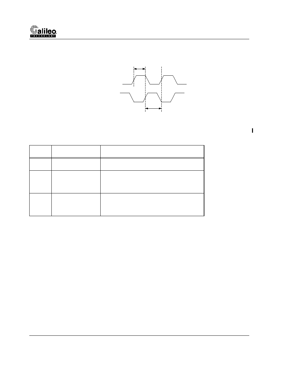
GT-64111 System Controller for RC4640, RM523X and VR4300 CPUs
124
Revision 1.0
Figure 26: TClk = PClk Skew Requirement
In addition to the above restriction, there are few sync modes specific restrictions, summarized in Table 32.
The sync mode can be programed by the CPU, the PCI or during autoload. For sync mode information, see Section
17.13.
TABLE 32. TClk/PClk Restrictions
Sync
Mode
PClk Frequency Range
Restrictions
0
from DC up to TClk
T
pclk
> T
tclk
+ 1.5ns, unless running with TClk = PClk
synchronized.
1
from TClk/2 up to TClk
f
pclk
> f
tclk
/2 + 1 MHz, unless running with synchro-
nized f
pclk
= f
tclk
/2 and minimum skew of 5.5ns
between PClk rise and every second TClk rise is
guarranteed.
2
from TClk/2 up to TClk
TClk and PClk are synchronized.
f
pclk
= f
tclk
/2 is allowed only if a minimum skew of
5.5ns between PClk rise and every second TClk rise
is guarranteed.
TClk
PClk
TClk to PClk
5 . 5 n s M i n i m u m S k e w
PClk to TClk
5 . 5 n s M i n i m u m S k e w
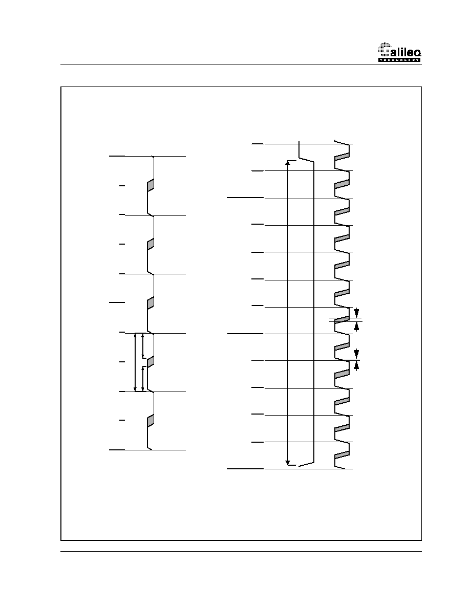
GT-64111 System Controller for RC4640, RM523X and VR4300 CPUs
Revision 1.0
Figure 27: TClk and Reset Timing Waveform
t6
0ns
10
0ns
20
0ns
Rs
t*
TClk
R
ese
t
t4
t5
t1
t2
t3
TClk
0ns
50n
s
TClk

GT-64111 System Controller for RC4640, RM523X and VR4300 CPUs
126
Revision 1.0
Figure 28: Block Write to DRAM, CasToRasWr = 1, CasWr = 0
Cm
d
A
ddr
DO
D1
D2
D3
D4
D5
D6
D7
D0
D1
D2
D3
D4
D5
D6
D7
Ro
w Ad
dr
es
s
Co
lu
m
n
A
d
d
r
e
s
s
0
1
2
3
4
5
6
7
t1
8
t1
7
t7
t1
1
t1
1
t1
2
t1
4
t2
2
t2
2
t1
5
t1
5
t2
1
t1
6
TCl
k
Va
li
dO
ut
*
Rel
eas
e*
Sys
Cm
d
S
ysA
D
V
ali
dI
n
*
Wr
Rdy
*
AD
DA
dr
BA
d
r
DWr
*
R
AS*
EC
AS
*
,
OC
A
S
*
LE
E,
LE
O
OE
E*
,
OE
O*

GT-64111 System Controller for RC4640, RM523X and VR4300 CPUs
Revision 1.0
Figure 29: Blcok Read from 32-bit Device, AccToFirst = 3, AccToNext = 3
Cm
d
A
ddr
D0
D1
D2
D3
D4
D5
D6
D7
A
ddr
D0
D1
D2
D3
D4
D5
D6
D7
0
1
2
3
4
5
6
7
D0
D1
D2
D3
D4
D5
D6
D7
t1
8
t1
7
t9
t9
t9
t9
t9
t1
4
t1
6
t1
2
t1
2
t1
5
t1
2
t1
4
t2
1
t1
6
t1
5
t1
5
TC
l
k
ValidOut
*
R
eleas
e*
S
y
sC
md
Sy
s
A
D
ValidI
n*
Wr
R
d
y*
ALE
AD
S
AD
BAdr
D
e
vR
W*
CS
*
C
S
T
i
m
ing*
EW
r*
,
OW
r*
LEE,
LEO
OEE*
,
OEO*
De
v
i
ce
Da
t
a

GT-64111 System Controller for RC4640, RM523X and VR4300 CPUs
128
Revision 1.0
21.
Functional Waveforms
Functional waveforms are not included in this datasheet. Transcribing waveforms from simulator outputs to "real world"
documentation is extremely error prone and we do not currently have a tool that can do it effectively. Rather than risk
introducing errors, Galileo Technology provides a seperate electronic document that included several dozen functional
waveforms. The waveform summary is available on our website: www.galileot.com (look in the "Library" area). Hard-
copies can also be ordered by contacting us at 408-451-1400.
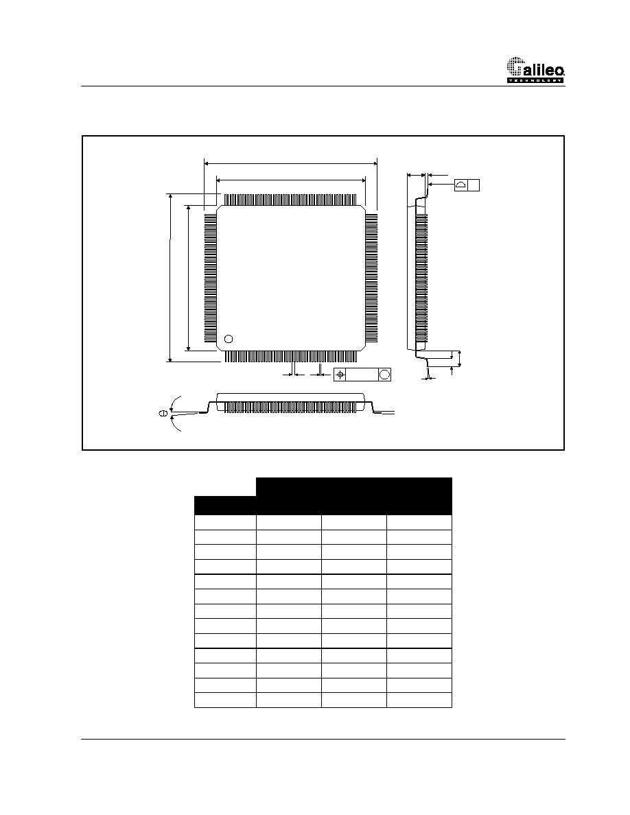
GT-64111 System Controller for RC4640, RM523X and VR4300 CPUs
Revision 1.0
22.
Packaging
Figure 30: 208 Lead PQFP Package Outline
Table 33: 208 PQFP Package Dimensions
M I L L I M E T E R S
SY M B OL
M I N .
N O M .
M A X .
A
1
0.05
0.25
0.50
A
2
3.17
3.32
3.47
b
0.10
0.20
0.30
c
0.10
0.15
0.20
D
27.90
28.00
28.10
E
27.90
28.00
28.10
e
0.50
Hd
30.35
30.60
30.85
He
30.35
30.60
30.85
L
0.45
0.60
0.75
L
1
1.30
Y
0.08
Q
0
7
A
1
He
E
Hd
D
b
A
2
L
L
1
0.08(0.003)
M
Y
e
c
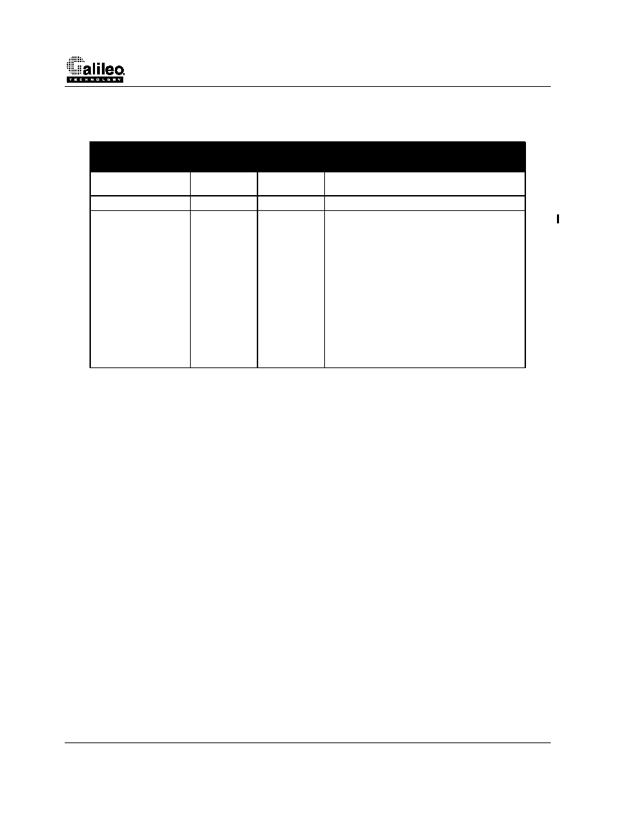
GT-64111 System Controller for RC4640, RM523X and VR4300 CPUs
130
Revision 1.0
23.
Revision History
Table 34: Document History
D o c u m e n t Ty p e
R e v.
N u m b e r
D a t e
C o m m e n t s
Product Review
0.9
1/19/98
First release, based on rev 1.3 GT-64011 spec.
Product Review
1.0
3/24/98
Second Release.
Data Sheet
1.1
FEB 4, 1999
1. Add TClk/PClk ratio restriction, Section 20.1.
2. CPU Restrictions, Section 3.8.
3. PCI parity support, Section 6.6.
4. Correct Device parameter regs initial values,
Section 17.8.
5. Add PCI sync modes clarification, Section
17.13.
6. Add 66MHz capable bit, Section 6.8 Section
17.15.
7 ICC specification, Section 19.3.
8. Thermal Data, Section 19.4.
9. PCI AC Timing Update. Minimum setup require-
ment change from 3ns to 4ns on PAD[31:0],
Frame*, IRdy*, TRdy*, DevSel*, Gnt*. All output
delays changed from 6ns to 7ns, Section 20.