
DA9124.004
24 April 2003
1 (12)
MAS9124
150 mA LDO Voltage Regulator IC
∑
Low Noise: 20 µVrms
∑
Low Minimum Output Capacitance
Requirement: 0.22 µF
∑
Excellent Ripple Rejection: 65 dB
∑
Very Low Dropout: 70 mV
∑
Regulator Enable/Disable Control
∑
Stable with Low-ESR Output
Capacitors
DESCRIPTION
MAS9124 is a low dropout voltage regulator with an
enable/disable pin, which allows device to be turned
off or on by pulling control to low or high.
Due to the low noise level of only 20 µVrms,
MAS9124 is suitable for sensitive circuits, e.g., in
portable applications. In addition to the noise levels,
MAS9124 excels in dropout voltage (70 mV typical
at 50 mA) and rise time (16 µs typical without
bypass capacitor). Also its ripple rejection ability of
65 dB at 10 kHz exceeds that of competition.
The Equivalent Series Resistance (ESR) range of
output capacitors that can be used with MAS9124 is
very wide. This ESR range from a few m up to a
couple of Ohms combined with no minimum output
current requirement makes the usage of MAS9124
easier and low in cost.
In order to save power the device goes into sleep
mode when the regulator is disabled. MAS9124 also
includes an auto-discharge function, wherein a
shutdown transistor turns on and discharges the
output capacitor. An internal thermal protection
circuit prevents the device from overheating. Also
the maximum output current is internally limited.
FEATURES
APPLICATIONS
∑
Low Noise
∑
Functionally and Pin Compatible with LP2985
∑
Can be used w/o C
BYPASS
, see p. 7
∑
Internal Thermal Shutdown
∑
Short Circuit Protection
∑
SOT23-5/WL-CSP Package
∑
Several Output Voltage Options Available,
see Ordering Information p. 11
∑
Cellular Phones
∑
Cordless Phones
∑
Accessories
∑
Pagers
∑
Battery Powered Systems
∑
Portable Systems
∑
Radio Control Systems
∑
Low Voltage Systems

DA9124.004
24 April 2003
2 (12)
PIN CONFIGURATION
SOT23-5
Top View
1
2
3
5
VIN
VOUT
CTRL
GND
BYPASS
24AX
4
For top marking information see
ordering information p. 11
WL-CSP
BOTTOM VIEW
A3
A1
C3
C1
B2
TOP VIEW
P
i
n A
1
D
e
s
i
gn
at
or
24XY
For top marking information see
ordering information p. 11
PIN DESCRIPTION
Pin Name
Pin Number
in SOT23-5
Pin Number in
WL-CSP
Pin Order 11
Note 1
Pin Number in
WL-CSP
Pin Order 12
Note 2
Type
Function
VIN
1
C3
C3
P
Power Supply Voltage
GND
2
B2
A1
G
Ground
CTRL
3
A1
A3
I
Enable/Disable Pin for Regulator
BYPASS
4
A3
B2
I
Pin for Bypass Capacitor
VOUT
5
C1
C1
O
Output
G = Ground, I = Input, O = Output, P = Power
Note 1:
WL-CSP Pin Order 11 is pin compatible with LP3985.
Note 2:
WL-CSP Pin Order 12 is pin compatible with LP2985.
A1
A3
B2
C1
C3

DA9124.004
24 April 2003
3 (12)
BLOCK DIAGRAM
CTRL
VIN
VOUT
GND
OVER CURRENT /
OVER TEMPERATURE
PROTECTION
VOLTAGE
REFERENCE
+
BYPASS
160k
SHUT-
DOWN
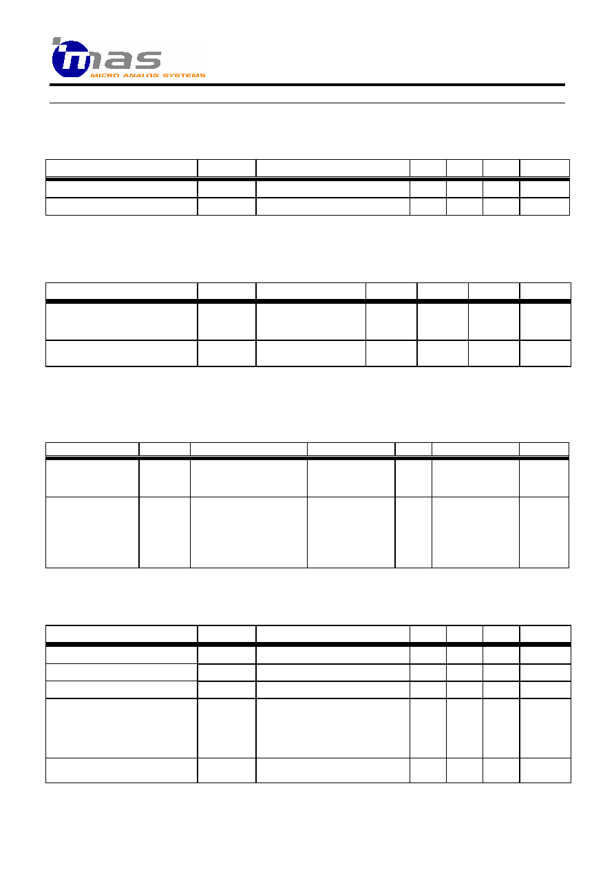
ABSOLUTE MAXIMUM RATINGS
All voltages with respect to ground
Parameter
Symbol
Conditions
Min
Max
Unit
Supply Voltage
V
IN
-0.3
6
V
Voltage Range for All Pins
-0.3
V
IN
+ 0.3
V
ESD Rating
HBM
2
kV
Junction Temperature
T
Jmax
+175
(limited)
∞C
Storage Temperature
T
S
-55
+150
∞C
Stresses beyond those listed may cause permanent damage to the device. The device may not operate under these conditions, but it will
not be destroyed.
RECOMMENDED OPERATING CONDITIONS
Parameter
Symbol
Conditions
Min
Max
Unit
Operating Junction
Temperature
T
J
-40
+125
∞C
Operating Ambient
Temperature
T
A
-40
+85
∞C
Operating Supply Voltage
V
IN
V
OUT(NOM)
< 5 V
V
OUT(NOM)
= 5 V
2.5
5.3
5.8
V
DA9124.004
24 April 2003
4 (12)
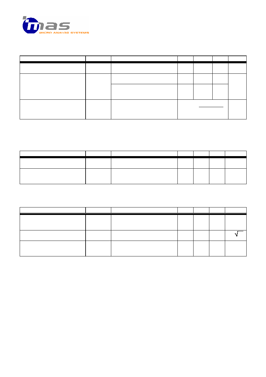
ELECTRICAL CHARACTERISTICS
x
Thermal Protection
T
A
= -40∞C to +85∞C, typical values at T
A
= +27∞C, V
IN
= V
OUT(NOM)
+ 1.0 V (or min 3.8 V), I
OUT
= 1.0 mA, C
IN
= 1.0 µF, C
L
= 1.0 µF,
C
BYPASS
= 10 nF, V
CTRL
= V
IN
, unless otherwise specified
Parameter
Symbol
Conditions
Min
Typ
Max
Unit
Threshold High
T
H
145
160
175
∞C
Threshold Low
T
L
135
150
165
∞C
The hysteresis of 10∞C prevents the device from turning on too soon after thermal shut-down.
x
Control Terminal Specifications
T
A
= -40∞C to +85∞C, typical values at T
A
= +27∞C, V
IN
= V
OUT(NOM)
+ 1.0 V (or min 3.8 V), I
OUT
= 1.0 mA, C
IN
= 1.0 µF, C
L
= 1.0 µF,
C
BYPASS
= 10 nF, V
CTRL
= V
IN
, unless otherwise specified
Parameter
Symbol
Conditions
Min
Typ
Max
Unit
Control Voltage
OFF State
(Note 1)
ON State
V
CTRL
-
0.3
1.6
0.55
V
IN
+ 0.3
V
Control Current
I
CTRL
V
CTRL
= V
IN
V
CTRL
= 0 V
5
0
10
µA
If CTRL-pin is not connected, MAS9124 is in OFF state (900 k pull-down resistor to ground).
Note 1:
If V
OUT(NOM)
= 5 V, the device should always be in the ON state.
x
Voltage Parameters
T
A
= -40∞C to +85∞C, typical values at T
A
= +27∞C, V
IN
= V
OUT(NOM)
+ 1.0 V (or min 3.8 V), I
OUT
= 1.0 mA, C
IN
= 1.0 µF, C
L
= 1.0 µF,
C
BYPASS
= 10 nF, V
CTRL
= V
IN
, unless otherwise specified
Parameter
Symbol
Conditions
Min
Typ
Max
Unit
Output Voltage
Tolerance
V
OUT
I
OUT
= 0 mA
I
OUT
= 150 mA
V
OUT(NOM)
-
0.05
V
OUT(NOM)
-
0.10
V
OUT(NOM)
+ 0.05
V
OUT(NOM)
+ 0.05
V
Dropout Voltage
V
DROP
I
OUT
= 1 mA
I
OUT
= 50 mA
I
OUT
= 150 mA
MAS9124A4 (150 mA)
MAS9124A5 (150 mA)
1.7
70
200
320
800
1100
mV
x
Current Parameters
T
A
= -40∞C to +85∞C, typical values at T
A
= +27∞C, V
IN
= V
OUT(NOM)
+ 1.0 V (or min 3.8 V), I
OUT
= 1.0 mA, C
IN
= 1.0 µF, C
L
= 1.0 µF,
C
BYPASS
= 10 nF, V
CTRL
= V
IN
, unless otherwise specified
Parameter
Symbol
Conditions
Min
Typ
Max
Unit
Continuous Output Current
I
OUT
150
mA
Short Circuit Current
I
MAX
R
L
= 0
200
450
675
mA
Peak Output Current
I
PK
V
OUT
> 95%* V
OUT(NOM)
410
mA
Ground Pin Current
I
GND
I
OUT
= 0 mA
I
OUT
= 10 mA
I
OUT
= 50 mA
I
OUT
= 150 mA
120
130
160
220
200
400
µA
Ground Pin Current, Sleep
Mode
I
GND
V
CTRL
= 0 V
0.01
5
µA
DA9124.004
24 April 2003
5 (12)
Power Dissipation
T
A
= -40∞C to +85∞C, typical values at T
A
= +27∞C, V
IN
= V
OUT(NOM)
+ 1.0 V (or min 3.8 V), I
OUT
= 1.0 mA, C
IN
= 1.0 µF, C
L
= 1.0 µF,
C
BYPASS
= 10 nF, V
CTRL
= V
IN
, unless otherwise specified
Parameter
Symbol
Conditions
Min
Typ
Max
Unit
Junction to Case Thermal
Resistance
R
JC
SOT23-5 package
81.0
∞C/W
typical PC board mounting,
still air, SOT23-5 package
255.9
Junction to Ambient Thermal
Resistance
R
JA
mounted on MAS9124 CSP
evaluation board,
WL-CSP package
210
∞C/W
Maximum Power Dissipation
P
d
any ambient temperature,
SOT23-5 package
JA
A
(MAX)
J
MAX
d
R
T
T
P
-
=
W
Note 1
Note 1
: T
J(MAX)
denotes maximum operating junction temperature (+125∞C), T
A
ambient temperature, and R
JA
junction-to-air thermal
resistance (+255.9∞C/W).
Line and Load Regulation
T
A
= -40∞C to +85∞C, typical values at T
A
= +27∞C, V
IN
= V
OUT(NOM)
+ 1.0 V (or min 3.8 V), I
OUT
= 1.0 mA, C
IN
= 1.0 µF, C
L
= 1.0 µF,
C
BYPASS
= 10 nF, V
CTRL
= V
IN
, unless otherwise specified
Parameter
Symbol
Conditions
Min
Typ
Max
Unit
Line Regulation
V
OUT(NOM)
+ 1 V < V
IN
< 5.3 V,
I
OUT
= 60 mA
0.7
mV
Load Regulation
I
OUT
= 1.0 to 50 mA
I
OUT
= 1.0 to 150 mA
5
10
mV
Noise and Ripple Rejection
T
A
= -40∞C to +85∞C, typical values at T
A
= +27∞C, V
IN
= V
OUT(NOM)
+ 1.0 V (or min 3.8 V), I
OUT
= 1.0 mA, C
IN
= 1.0 µF, C
L
= 1.0 µF,
C
BYPASS
= 10 nF, V
CTRL
= V
IN
, unless otherwise specified
Parameter
Symbol
Conditions
Min
Typ
Max
Unit
Output Noise Voltage
V
RMS
300Hz < f < 50kHz
C
BYPASS
= 10 nF
w/o C
BYPASS
20
110
µVrms
Noise Density
V
N
I
OUT
= 50 mA,
f = 1.0 kHz
100
nV
/
Hz
PSRR
f = 1 kHz
f = 10 kHz
f = 100 kHz
67
65
48
dB