DA9125.004
17 February, 2000
1
MAS9125
5 Outputs LDO Voltage Regulator IC
∑
Five Low Dropout Voltage Regulators
∑
Enable/Disable Control Pin for Each
Regulator
∑
Common Control Pin to Shutdown The
Whole Circuit
∑
All Outputs Ultra Low Noise
∑
Excellent Ripple Rejection
∑
Very Low Quiescent Current
∑
Thermal and Current Limiting Protection
DESCRIPTION
The MAS9125 is a voltage regulator IC with five
2.8 V ultra low noise LDO regulators. Each regulator
has its own independent enable/disable control pin.
Additionally, all the outputs can be turned off by
using a common control pin, which overrides
regulator specific control pins. The highest output
current is 150 mA (for the output 4). MAS9125
features a very low quiescent current: max 5
µ
A in
Off State and 90
µ
A in On State. The dropout
voltage is typically 0.11 V for outputs 1, 2, 3, and 5
and 0.17 V for output 4. The regulators 1, 2, and 3
have a common power supply pin marked as
VCC_1. VCC_2 functions as a power supply pin for
the regulators 4 and 5.
MAS9125 excels especially in noise performance
and ripple rejection. Since all the outputs exhibit
ultra low noise, noise sensitive circuitry can be
driven by any of them. With high ripple rejection,
MAS9125 effectively shields downstream
electronics against power line disturbances.
An internal thermal protection circuit prevents the
device from overheating. The maximum output
current is limited internally, too.
FEATURES
APPLICATIONS
∑
2.8 V Regulators at 30 mA, 40 mA, 50 mA,
150 mA, and 60 mA
∑
Excellent Ripple Rejection: 72 dB Typical at 1
kHz, and 52 dB Typical at 10 kHz
∑
Ultra Low Noise: 21
µ
Vrms Typical and
30
µ
Vrms Maximum for All Regulators over
Frequency Range 100 Hz...100 kHz
∑
Fast Dynamic Response
∑
Output Voltage Accuracy <
±
1.7% at 27
o
C
∑
100 nF for Output Capacitors 1, 2, 4, and 5 and
1
µ
F for Output Capacitor 3
∑
Separate Enable/Disable Control for Each
Output
∑
Common Control Pin to Shutdown the Whole IC
∑
Very Low Quiescent Current: Maximum 5
µ
A in
Off State (Independent & Common Controls
Off), Typical 90
µ
A in On State (Common
Control On, Independent Controls Off)
∑
TSSOP16
Package
∑
Functionally and Pin Compatible with MC33765
∑
Mobile
Phones
∑
Cordless
Phones
∑
Portable
Systems
∑
Battery Powered Systems
∑
Systems Needing Stabilized Power in Separate
Blocks
DA9125.004
17 February, 2000
2
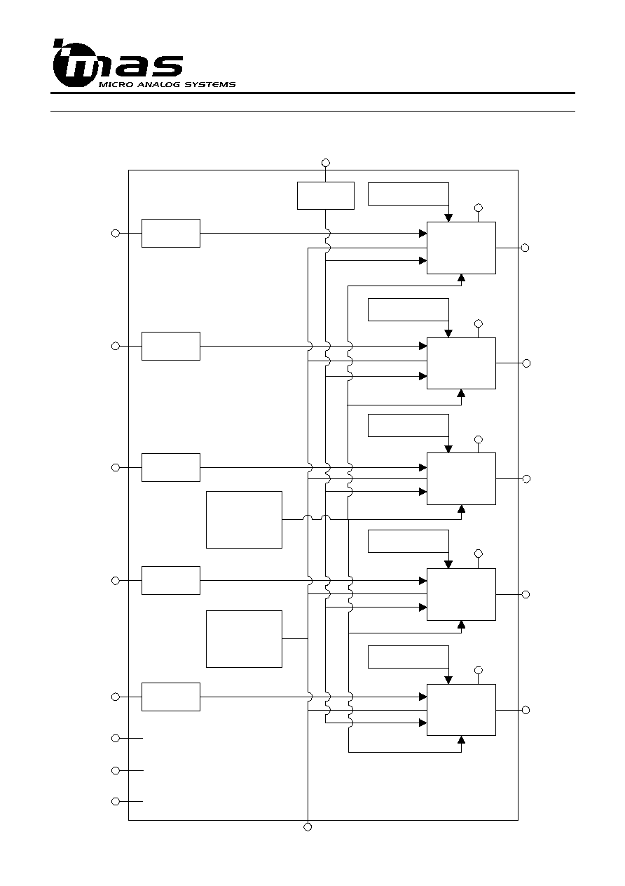
BLOCK DIAGRAM
LDO_1
LDO_2
LDO_3
LDO_4
LDO_5
Current Limit
Current Limit
Current Limit
Current Limit
Current Limit
Bandgap
Reference
Temperature
Protection
Control
Control
Control
Control
Control
CTRL_1
CTRL_2
CTRL_3
CTRL_4
CTRL_5
Common
Control
VCC_2
VCC_2
VCC_1
VCC_1
VCC_1
VOUT_1
VOUT_2
VOUT_3
VOUT_4
VOUT_5
BYPASS
VCC_1
VCC_2
GND
COMMON_CTRL

DA9125.004
17 February, 2000
3
PIN CONFIGURATION & TOP MARKING
PIN DESCRIPTION
Pin Name
Pin
Type
Function
BYPASS
1
I
Noise Bypass
COMMON_CTRL
2
I
Control Pin to Shutdown the Whole IC
(Logic 0 = Shutdown, Logic 1 = Enable Regulator Specific Control Pins)
CTRL_1
3
I
Enable/Disable Control for Regulator 1
CTRL_2
4
I
Enable/Disable Control for Regulator 2
CTRL_3
5
I
Enable/Disable Control for Regulator 3
CTRL_4
6
I
Enable/Disable Control for Regulator 4
CTRL_5
7
I
Enable/Disable Control for Regulator 5
GND
8
P
Ground
VOUT_5
9
O
2.8 V/60 mA Regulator Output
VCC_2
10
P
Power Supply Voltage
VOUT_4
11
O
2.8 V/150 mA Regulator Output
VOUT_3
12
O
2.8 V/50 mA Regulator Output
VOUT_2
13
O
2.8 V/40 mA Regulator Output
VOUT_1
14
O
2.8 V/30 mA Regulator Output
VCC_1
15
P
Power Supply Voltage
NC
16
Not Connected
I = Input, O = Output, P = Power
COMMON_CTRL
BYPASS
CTRL_1
CTRL_2
CTRL_3
CTRL_4
CTRL_5
GND
VOUT_1
NC
VCC_1
VOUT_2
VOUT_3
VOUT_4
VCC_2
VOUT_5
91
2
5
B
YY
W
W
Top Marking Definitions:
YYWW = Year Week
DA9125.004
17 February, 2000
4
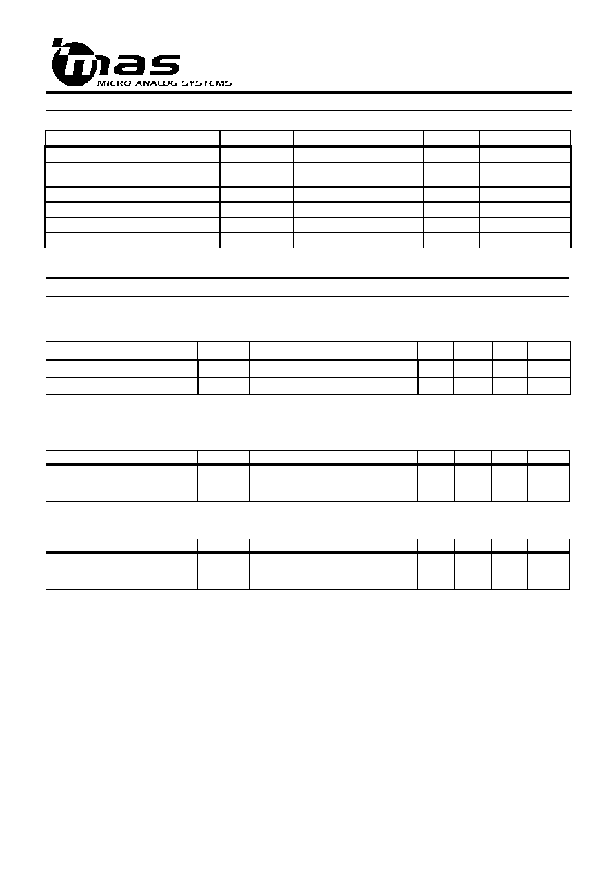
ABSOLUTE MAXIMUM RATINGS
All Voltages with Respect to Ground
Parameter
Symbol
Conditions
Min
Max
Unit
Power Supply Voltage
V
CC
6
V
Thermal Resistance
(Junction-to-Air)
R
JA
144
∞C/W
Operating Junction Temperature
125
∞C
Junction Temperature
T
J
175
o
C
Operating Ambient Temperature
T
A
-40
+85
∞C
Storage Temperature
T
S
-55
+150
o
C
Stresses beyond those listed may cause permanent damage to the device. The device may not operate under these conditions, but will not
be destroyed.
ELECTRICAL CHARACTERISTICS
For typical values T
A
= 27
o
C, for min/max values T
A
= -40
o
C to +85
o
C, unless otherwise noted
x
Thermal Protection
Parameter
Symbol
Conditions
Min
Typ
Max
Unit
Threshold High
T
H
150
160
170
o
C
Threshold Low
T
L
140
150
160
o
C
A hysteresis of 10
o
C prevents oscillation in case of thermal shutdown. After the regulator temperature has dropped by this value, it will turn
on again automatically.
x
Common Control Pin Parameters
Parameter
Symbol
Conditions
Min
Typ
Max
Unit
Input Voltage
ON-state
OFF-state
V
C-CTRL
0
2.0
V
CC
0.3
V
x
Single Regulator Control Pin Parameters
Parameter
Symbol
Conditions
Min
Typ
Max
Unit
Input Voltage
ON-state
OFF-state
V
CTRL1..5
0
2.0
V
cc
0.3
V

DA9125.004
17 February, 2000
5
x
Current Parameters
Parameter
Symbol
Conditions
Min
Typ
Max
Unit
Regulator 1 Output Current
I
OUT1
0.5
30
mA
Regulator 2 Output Current
I
OUT2
0.5
40
mA
Regulator 3 Output Current
I
OUT3
0
50
mA
Regulator 4 Output Current
I
OUT4
0.5
150
mA
Regulator 5 Output Current
I
OUT5
Listed maximum output currents
are peak values. Maximum power
dissipation should be used to
determine the maximum total DC
current.
0.5
60
mA
Current Limit
I
MAX1..5
I
OUT
refers to each regulators'
maximum output current I
OUT1..5
3xI
OUT
mA
Quiescent Current
IQ
OFF
I
OUT
= 0 A, V
C-CTRL
< 0.3 V,
V
CTRL1..5
< 0.3 V
5
µ
A
Quiescent Current
IQ
ON
I
OUT
= 0 A, V
C-CTRL
> 2.0 V,
V
CTRL1..5
> 2.0 V
500
µ
A
Quiescent Current
IQ
C-ON
I
OUT
= 0 A, V
C-CTRL
> 2.0 V,
V
CTRL1..5
< 0.3 V
90
µ
A
Total RMS Output Current
I
RMS
T
A
= 85 ∞C, V
CC
= 5.3 V
110
mA
Total RMS Output Current
I
RMS
T
A
= 25 ∞C, V
CC
= 5.3 V
250
mA
x
Power Dissipation
Parameter
Symbol
Conditions
Min
Typ
Max
Unit
Power Dissipation
P
d
V
CC
= 5.3 V, T
A
= 85
∞
C
285
mW
Power Dissipation
P
d
V
CC
= 5.3 V, T
A
= 25
∞
C
700
mW
x
Voltage Parameters
Parameter
Symbol
Conditions
Min
Typ
Max
Unit
Supply Voltage
V
CC1..2
3.0
3.6
5.3
V
Output Voltage
V
OUT1..5
2.7
2.8
2.85
V
Regulator 1 Dropout Voltage
V
DROP1
I
OUT1
= 25 mA for Typical V
DROP1
I
OUT1
= Max for Max V
DROP1
0.11
0.17
V
Regulator 2 Dropout Voltage
V
DROP2
I
OUT2
= 35 mA for Typical V
DROP2
I
OUT2
= Max for Max V
DROP2
0.11
0.17
V
Regulator 3 Dropout Voltage
V
DROP3
I
OUT3
= 40 mA for Typical V
DROP3
I
OUT3
= Max for Max V
DROP3
0.11
0.17
V
Regulator 4 Dropout Voltage
V
DROP4
I
OUT4
= 140 mA for Typical V
DROP4
I
OUT4
= Max for Max V
DROP4
0.17
0.30
V
Regulator 5 Dropout Voltage
V
DROP1
I
OUT5
= 40 mA for Typical V
DROP5
I
OUT5
= Max for Max V
DROP5
0.11
0.17
V
x
External Capacitors
Parameter
Symbol
Conditions
Min
Typ
Max
Unit
Output Capacitors for
Regulators 1, 2, 4, 5
Regulator 3
C
OUT1..5
C
OUT3
0.10
1
1
µ
F
Effective Series Resistance
ESR
0.05
1
3
Bypass Capacitor
C
BYPASS
100
nF