DA9161.006
1 April 2003
1 (15)
MAS9161
80 mA LDO Voltage Regulator IC
∑
Only 10.5 µA Ground Pin Current
at 1 mA Load Current
∑
Good Transient Performance
∑
Low Dropout Voltage: 200 mV
∑
Low Noise
∑
Enable/Disable Control
∑
Stable with Low-ESR Output
Capacitors
DESCRIPTION
MAS9161 LDO voltage regulator is optimized for
operation at low ground pin current of just 10.5 µA.
This combined with the good overall performance
makes MAS9161 very suitable for providing
continuous supply in low power circuits. The
performance of MAS9161 benefits applications
where standby periods are long and where long
battery life is essential.
In addition to the low ground pin current, MAS9161
excels in dropout voltage (200 mV typical at 80 mA).
Even though MAS9161 does not use an external
bypass capacitor, the noise level (100
Hz...
100
kHz) is only 70
µVrms with 1
µF output
capacitor.
The Equivalent Series Resistance (ESR) range of
output capacitors that can be used with MAS9161 is
very wide. This ESR range from zero up to a couple
of Ohms combined with no minimum output current
requirement makes the usage of MAS9161 easier
and low in cost.
Enable/disable pin allows MAS9161 to be turned off
and on. In order to save power the device enters the
sleep mode when the regulator is disabled.
An internal thermal protection circuit prevents the
device from overheating. Also the maximum output
current is internally limited.
FEATURES
APPLICATIONS
∑
Extremely Low Current Consumption
∑
Good Transient Performance
∑
Output Accuracy <
±
3.3%
∑
Internal Thermal Shutdown
∑
Short Circuit Protection
∑
Thin SOT (TSOT-5) or WL-CSP Package
∑
Several Output Voltage Options Available,
see Ordering Information p. 14
∑
Continuously Working Low Power Circuits
∑
Digital Circuits
∑
Real-Time Clocks (RTC)
∑
SRAMs
∑
CMOS Backup Power
∑
Cellular Phones
∑
Portable Systems
∑
Smoke Detectors

DA9161.006
1 April 2003
2 (15)
PIN CONFIGURATION
TSOT-5
Top view
1
2
3
5
VIN
VOUT
CTRL
GND
N/C
61AX
4
For top marking information see
ordering information p. 14
WL-CSP
BOTTOM VIEW
A3
A1
C3
C1
B2
TOP VIEW
P
i
n A
1
D
e
s
i
gn
at
or
61XY
For top marking information see
ordering information p. 14
PIN DESCRIPTION
Pin Name
Pin
Number in
TSOT-5
Pin
Number in
WL-CSP
Type
Function
VIN
1
C3
P
Power Supply Voltage
GND
2
A1
G
Ground
CTRL
3
A3
I
Enable/Disable Pin for Regulator
N/C
4
B2
-
Not Connected
VOUT
5
C1
O
Output
G = Ground, I = Input, O = Output, P = Power
A1
A3
B2
C1
C3
DA9161.006
1 April 2003
3 (15)
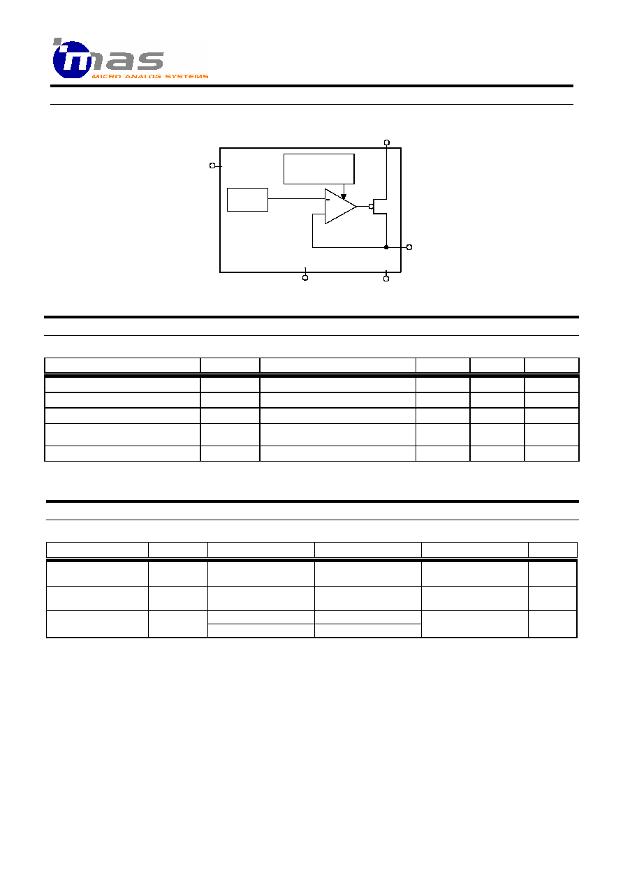
BLOCK DIAGRAM
ABSOLUTE MAXIMUM RATINGS
All voltages with respect to ground.
Parameter
Symbol
Conditions
Min
Max
Unit
Supply Voltage
V
IN
-0.3
6
V
Voltage Range for All Pins
-0.3
V
IN
+ 0.3
V
ESD Rating
HBM
2
kV
Junction Temperature
T
Jmax
+175
(limited)
∞C
Storage Temperature
T
S
-55
+150
∞C
Stresses beyond those listed may cause permanent damage to the device. The device may not operate under these conditions, but it will
not be destroyed.
RECOMMENDED OPERATING CONDITIONS
All voltages with respect to ground.
Parameter
Symbol
Conditions
Min
Max
Unit
Operating Junction
Temperature
T
J
-40
+125
∞C
Operating Ambient
Temperature
T
A
-40
+85
∞C
V
OUT(NOM)
+ 0.3 V
Operating Supply
Voltage
V
IN
For MAS9161A4
2.5
5.3
V
CTRL
VIN
VOUT
GND
OVER CURRENT /
OVER TEMPERATURE
PROTECTION
VOLTAGE
REFERENCE
+
N/C

DA9161.006
1 April 2003
4 (15)
ELECTRICAL CHARACTERISTICS
x
Thermal Protection
T
A
= -40∞C to +85∞C, typical values at T
A
= +27∞C, V
IN
= V
OUT(NOM)
+ 1 V, I
OUT
= 1 mA, C
IN
= 1.0 µF, C
L
= 1.0 µF, V
CTRL
= 2 V, unless
otherwise specified.
Parameter
Symbol
Conditions
Min
Typ
Max
Unit
Threshold
T
130
150
175
∞C
x
Control Terminal Specifications
T
A
= -40∞C to +85∞C, typical values at T
A
= +27∞C, V
IN
= V
OUT(NOM)
+ 1 V, I
OUT
= 1 mA, C
IN
= 1.0 µF, C
L
= 1.0 µF, V
CTRL
= 2 V, unless
otherwise specified.
Parameter
Symbol
Conditions
Min
Typ
Max
Unit
Control Voltage
OFF State
ON State
V
CTRL
-0.3
1.2
0.5
V
IN
+ 0.3
V
Control Current
I
CTRL
V
CTRL
= 1.2 V
V
CTRL
= 2.0 V
V
CTRL
= 3.8 V
0.35
0.70
1.50
1.5
µA
If CTRL-pin is not connected, MAS9161 is in OFF state (4 M pull-down resistor to ground).
x
Voltage Parameters
T
A
= -40∞C to +85∞C, typical values at T
A
= +27∞C, V
IN
= V
OUT(NOM)
+ 1 V, I
OUT
= 1 mA, C
IN
= 1.0 µF, C
L
= 1.0 µF, V
CTRL
= 2 V, unless
otherwise specified.
Parameter
Symbol
Conditions
Min
Typ
Max
Unit
Output Voltage
Tolerance
V
OUT
I
OUT
= 0 mA
I
OUT
= 50 mA
V
OUT(NOM)
≠ 0.06
V
OUT(NOM)
≠ 0.08
V
OUT(NOM)
+ 0.06
V
OUT(NOM)
+ 0.06
V
Dropout Voltage
V
DROP
I
OUT
= 1 mA
I
OUT
= 10 mA
I
OUT
= 50 mA
I
OUT
= 80 mA
5
50
150
200
mV
x
Current Parameters
T
A
= -40∞C to +85∞C, typical values at T
A
= +27∞C, V
IN
= V
OUT(NOM)
+ 1 V, I
OUT
= 1 mA, C
IN
= 1.0 µF, C
L
= 1.0 µF, V
CTRL
= 2 V, unless
otherwise specified.
Parameter
Symbol
Conditions
Min
Typ
Max
Unit
Continuous Output Current
I
OUT
0
80
mA
Short Circuit Current
I
MAX
R
L
= 0
240
mA
Peak Output Current
I
PK
V
OUT
> 95% * V
OUT(NOM)
120
mA
Ground Pin Current
I
GND
V
CTRL
= 2.0 V
I
OUT
= 0 mA
I
OUT
= 1 mA
I
OUT
= 10 mA
I
OUT
= 80 mA
10
10.5
16
61
µA
T
A
= + 27∞C
0.01
0.5
Ground Pin Current, Sleep
Mode
I
GND
V
CTRL
= 0 V
T
A
= + 85∞C
0.2
4
µA

DA9161.006
1 April 2003
5 (15)
x
Power Dissipation
T
A
= -40∞C to +85∞C, typical values at T
A
= +27∞C, V
IN
= V
OUT(NOM)
+ 1 V, I
OUT
= 1 mA, C
IN
= 1.0 µF, C
L
= 1.0 µF, V
CTRL
= 2 V, unless
otherwise specified.
Parameter
Symbol
Conditions
Min
Typ
Max
Unit
thermal test board according
to JC51-7 (4 layers),
TSOT-5 package
85
Thermal Resistance
(Junction-to-Air)
R
JA
mounted on MAS9161 CSP
evaluation board,
WL-CSP package
TBD
∞C/W
Maximum Power Dissipation
P
d
any ambient temperature,
TSOT-5 package
JA
A
(MAX)
J
MAX
d
R
T
T
P
-
=
W
Note 1
Note 1: T
J(MAX)
denotes maximum operating junction temperature (+125∞C), T
A
ambient temperature, and R
JA
junction-to-air thermal
resistance (+85∞C/W).
x
Line and Load Regulation
T
A
= -40∞C to +85∞C, typical values at T
A
= +27∞C, V
IN
= V
OUT(NOM)
+ 1 V, I
OUT
= 1 mA, C
IN
= 1.0 µF, C
L
= 1.0 µF, V
CTRL
= 2 V, unless
otherwise specified.
Parameter
Symbol
Conditions
Min
Typ
Max
Unit
Line Regulation
V
OUT(NOM)
+ 1 V < V
IN
< 5.3 V,
I
OUT
= 10 mA
1.0
3
mV
Load Regulation
I
OUT
= 1 mA to 80 mA
12
24
mV
x
Noise and Ripple Rejection
T
A
= -40∞C to +85∞C, typical values at T
A
= +27∞C, V
IN
= V
OUT(NOM)
+ 1 V, I
OUT
= 1 mA, C
IN
= 1.0 µF, C
L
= 1.0 µF, V
CTRL
= 2 V, unless
otherwise specified.
Parameter
Symbol
Conditions
Min
Typ
Max
Unit
Output Noise Voltage
V
RMS
100 Hz < f < 100 kHz,
I
OUT
= 10 mA
70
µVrms
Noise Density
V
N
I
OUT
= 10 mA,
f = 10 kHz
300
nV
/
Hz
I
OUT
= 1 mA
f = 1 kHz
f = 10 kHz
f = 100 kHz
50
30
30
dB
PSRR
I
OUT
= 10 mA
f = 1 kHz
f = 10 kHz
f = 100 kHz
50
30
30
dB