DA9162.003
13 March 2003
1 (10)
MAS9162
80 mA
LDO Voltage Regulator IC
∑
Low Noise, 30 µVrms, without
External Bypass Capacitor
∑
Very Short Start-up Time: 10 µs
∑
Stable with Low-ESR Output
Capacitors
∑
Low Minimum Output Capacitance
Requirement: 0.25 µF
∑
Regulator Enable/Disable Control
DESCRIPTION
MAS9162 is a low dropout voltage regulator, which
achieves the low output noise level of 30 µVrms
without an external bypass capacitor. MAS9162
features very fast start-up time (typically only 10 µs
from start-up to within ±1% of V
OUT(NOM)
) and low
dropout voltage (80 mV typical at 50 mA).
The minimum output capacitance requirement is
very low. This with the very short start-up time
makes it possible to switch the regulator off and on
even in timing critical and/or noise sensitive
applications. In order to save power the device
enters the sleep mode when the regulator is
disabled.
The Equivalent Series Resistance (ESR) range of
output capacitors that can be used with MAS9162 is
very wide. This ESR range from a few m up to a
couple of Ohms combined with no minimum output
current requirement makes the usage of MAS9162
easier and low in cost.
An internal thermal protection circuit prevents the
device from overheating. Also the maximum output
current is internally limited.
FEATURES
APPLICATION
∑
No External Bypass Capacitor Needed
∑
Optimized for Fast Start-up
∑
Internal Thermal Shutdown
∑
Short Circuit Protection
∑
SOT23-5 Package
∑
Pin Compatible with MC33761
∑
Several Output Voltage Options Available, see
Ordering Information p. 10
∑
RF-Oscillators
∑
Cellular Phones
∑
Cordless Phones
∑
Pagers
∑
Battery Powered Systems
∑
Portable Systems
∑
Radio Control Systems
PIN CONFIGURATION
Top View
For Top Marking Information
see Ordering Information p. 10
1
2
3
5
VIN
VOUT
CTRL
GND
NC
62AX
4

DA9162.003
13 March 2003
2 (10)
PIN DESCRIPTION
Pin Name
Pin
Type
Function
VIN
1
P
Power Supply Voltage
GND
2
G
Ground
CTRL
3
I
Enable/Disable Pin for Regulator
N/C
4
-
Not Connected
VOUT
5
O
Output
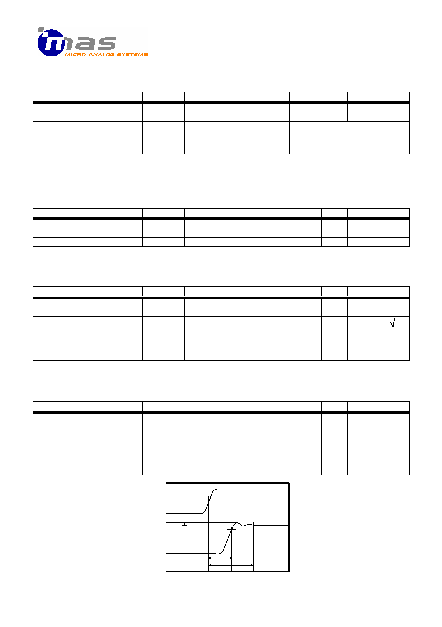
BLOCK DIAGRAM
ABSOLUTE MAXIMUM RATINGS
All voltages with respect to ground.
Parameter
Symbol
Conditions
Min
Max
Unit
Supply Voltage
V
IN
-0.3
6
V
Voltage Range for All Pins
-0.3
V
IN
+ 0.3
V
ESD Rating
HBM
2
kV
Junction Temperature
T
Jmax
+175
(limited)
∞C
Storage Temperature
T
S
-55
+150
∞C
Stresses beyond those listed may cause permanent damage to the device. The device may not operate under these conditions, but it will
not be destroyed.
RECOMMENDED OPERATING CONDITIONS
All voltages with respect to ground.
Parameter
Symbol
Conditions
Min
Max
Unit
Operating Junction
Temperature
T
J
- 40
+125
∞C
Operating Ambient
Temperature
T
A
-40
+85
∞C
Operating Supply Voltage
V
IN
V
OUT(NOM)
+ 0.3
5.3
V
G = Ground, I = Input, O = Output, P = Power
CTRL
VIN
VOUT
GND
OVER CURRENT /
OVER TEMPERATURE
PROTECTION
VOLTAGE
REFERENCE
+

DA9162.003
13 March 2003
3 (10)
ELECTRICAL CHARACTERISTICS
x
Thermal Protection
T
A
= -40∞C to +85∞C, typical values at T
A
= +27∞C, V
IN
= V
OUT(NOM)
+ 1 V, I
OUT
= 1 mA, C
IN
= 1.0 µF, C
OUT
= 1.0 µF, V
CTRL
= 2 V, unless
otherwise specified.
Parameter
Symbol
Conditions
Min
Typ
Max
Unit
Threshold High
T
H
145
160
175
∞C
Threshold Low
T
L
135
150
165
∞C
The hysteresis of 10
o
C prevents the device from turning on too soon after thermal shut-down.
x
Control Terminal Specifications
T
A
= -40∞C to +85∞C, typical values at T
A
= +27∞C, V
IN
= V
OUT(NOM)
+ 1 V, I
OUT
= 1 mA, C
IN
= 1.0 µF, C
OUT
= 1.0 µF, V
CTRL
= 2 V, unless
otherwise specified.
Parameter
Symbol
Conditions
Min
Typ
Max
Unit
Control Voltage
OFF State
ON State
V
CTRL
-0.3
1.6
0.55
V
IN
+ 0.3
V
Control Current
I
CTRL
V
CTRL
= V
IN
V
CTRL
= 0 V
5
0
15
µA
If CTRL-pin is not connected, MAS9162 is in OFF state (1 M
pull-down resistor to ground).
Voltage Parameters
T
A
= -40∞C to +85∞C, typical values at T
A
= +27∞C, V
IN
= V
OUT(NOM)
+ 1 V, I
OUT
= 1 mA, C
IN
= 1.0 µF, C
OUT
= 1.0 µF, V
CTRL
= 2 V, unless
otherwise specified.
Parameter
Symbol
Conditions
Min
Typ
Max
Unit
Output Voltage
Tolerance
V
OUT
I
OUT
= 0 mA
I
OUT
= 50 mA
V
OUT(NOM)
≠ 0.05
V
OUT(NOM)
≠ 0.10
V
OUT(NOM)
+ 0.07
V
OUT(NOM)
+ 0.05
V
Dropout Voltage
V
DROP
I
OUT
= 1 mA
I
OUT
= 10 mA
I
OUT
= 50 mA
46
51
80
mV
x
Current Parameters
T
A
= -40∞C to +85∞C, typical values at T
A
= +27∞C, V
IN
= V
OUT(NOM)
+ 1 V, I
OUT
= 1 mA, C
IN
= 1.0 µF, C
OUT
= 1.0 µF, V
CTRL
= 2 V, unless
otherwise specified.
Parameter
Symbol
Conditions
Min
Typ
Max
Unit
Continuous Output Current
I
OUT
0
80
mA
Short Circuit Current
I
MAX
R
L
= 0
230
mA
Peak Output Current
I
PK
V
OUT
> 95% * V
OUT(NOM)
180
mA
Ground Pin Current
I
GND
I
OUT
= 0 mA
I
OUT
= 10 mA
I
OUT
= 50 mA
190
260
300
250
350
400
µA
T
A
= 25∞C
0.02
0.5
Ground Pin Current, Sleep
Mode
I
GND
V
CTRL
= 0 V
T
A
= 85∞C
0.2
2
µA
DA9162.003
13 March 2003
4 (10)
Power Dissipation
T
A
= -40∞C to +85∞C, typical values at T
A
= +27∞C, V
IN
= V
OUT(NOM)
+ 1 V, I
OUT
= 1 mA, C
IN
= 1.0 µF, C
OUT
= 1.0 µF, V
CTRL
= 2 V, unless
otherwise specified.
Parameter
Symbol
Conditions
Min
Typ
Max
Unit
Thermal Resistance
(Junction-to-Air)
R
JA
thermal test board according
to SEMI G42-88 (single layer)
255.9
∞C/W
Maximum Power Dissipation
P
d
any ambient temperature
JA
A
(MAX)
J
MAX
d
R
T
T
P
-
=
W
Note 1
Note 1: T
J(MAX)
denotes maximum operating junction temperature (+125∞C), T
A
ambient temperature, and R
JA
junction-to-air thermal
resistance (+255.9∞C/W).
Line and Load Regulation
T
A
= -40∞C to +85∞C, typical values at T
A
= +27∞C, V
IN
= V
OUT(NOM)
+ 1 V, I
OUT
= 1 mA, C
IN
= 1.0 µF, C
OUT
= 1.0 µF, V
CTRL
= 2 V, unless
otherwise specified.
Parameter
Symbol
Conditions
Min
Typ
Max
Unit
Line Regulation
V
OUT(NOM)
+ 1 V < V
IN
< 5.3 V
I
OUT
= 50 mA
0.75
2.5
mV
Load Regulation
I
OUT
= 1 mA to 50 mA
13.5
25
mV
Noise and Ripple Rejection
T
A
= -40∞C to +85∞C, typical values at T
A
= +27∞C, V
IN
= V
OUT(NOM)
+ 1 V, I
OUT
= 1 mA, C
IN
= 1.0 µF, C
OUT
= 1.0 µF, V
CTRL
= 2 V, unless
otherwise specified.
Parameter
Symbol
Conditions
Min
Typ
Max
Unit
Output Noise Voltage
V
RMS
100 Hz < f < 100 kHz
30
µVrms
Noise Density
V
N
I
OUT
= 50 mA,
f = 10 kHz
140
nV/ Hz
PSRR
f = 1 kHz
f = 10 kHz
f = 100 kHz
56
46
46
dB
x
Dynamic Parameters
T
A
= -40∞C to +85∞C, typical values at T
A
= +27∞C, V
IN
= V
OUT(NOM)
+ 1 V, I
OUT
= 1 mA, C
IN
= 1.0 µF, C
OUT
= 1.0 µF, V
CTRL
= 2 V, unless
otherwise specified.
Parameter
Symbol
Conditions
Min
Typ
Max
Unit
Start-up Delay (from start-up
to 80% of V
OUT(NOM)
)
V
CTRL
= 0 to 2.4 V, I
OUT
= 50 mA,
C
L
1.0 µF
7.5
µs
Overshoot
V
CTRL
= 0 to 2.4 V
1.0
8.0
%
Start-up Time
(settling time of voltage
transient from start-up to
within
±
1% of V
OUT(NOM)
)
V
CTRL
= 0 to 2.4 V, I
OUT
= 50 mA
C
L
1.0 µF
10
µs
CTRL
VOUT
50%
start-up delay
80%
overshoot
start-up time
Figure1.
Definitions of
start-up delay, overshoot
and start-up time.
DA9162.003
13 March 2003
5 (10)
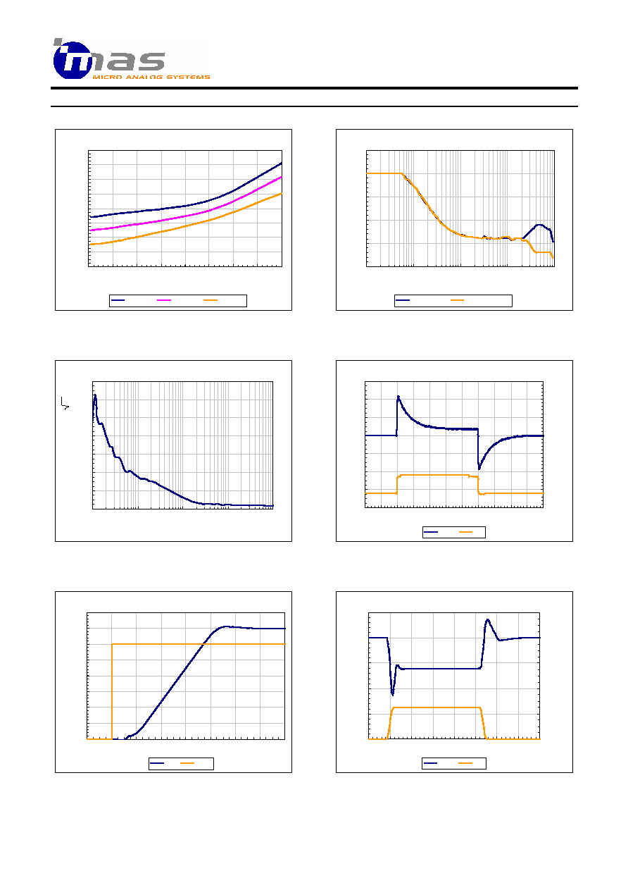
TYPICAL PERFORMANCE CHARACTERISTICS
DUT = MAS9162AST2, V
IN
= 3.8 V, T
A
= +27∞C, I
OUT
= 50 mA, C
IN
= 1.0 µF, C
L
= 1.0 µF, V
CTRL
= 2 V, unless otherwise specified.
MAS9162 Dropout voltage vs. load current
0
20
40
60
80
100
120
140
160
0
10
20
30
40
50
60
70
80
Load current (mA)
D
r
o
p
o
ut
vo
l
t
age (
m
V
)
T = +85∞C
T = +25∞C
T= -40∞C
MAS9162 PSRR vs. frequency
40
45
50
55
60
65
100
1000
10000
100000
1000000
Frequency (Hz)
P
S
RR (d
B)
Cload = 1 µF
Cload = 470 nF
Figure 2. Dropout voltage vs. load current and temperature.
Figure 3. PSRR vs. frequency. Signal source used:
C
IN
= 0 µF, R
SOURCE
= 50 .
MAS9162 Noise spectral density
0
200
400
600
800
1000
1200
1400
100
1000
10000
100000
1000000
Frequency (Hz)
N
o
i
se s
p
ect
r
a
l
d
e
n
s
i
t
y (
n
V
/
H
z
Ω
)
N
o
i
se sp
ect
r
a
l
d
e
n
s
i
t
y
(
n
V
/
Hz
)
MAS9162 Line transient response
-8
-6
-4
-2
0
2
4
6
Time (50 µs/div)
V
OU
T
(m
V
)
3
4
5
6
7
8
9
10
V
IN
(V
)
Vout
Vin
Figure 4. Output noise spectral density.
Figure 5. Line transient response. Signal source used:
C
IN
= 0 µF, R
SOURCE
= 50 , V
IN
= 3.8 V...4.8 V in 2 µs.
MAS9162 Start-up
0
0.4
0.8
1.2
1.6
2
2.4
2.8
3.2
Time (2 µs/div)
V
o
l
t
ag
e (
V
)
Vout
CTRL
MAS9162 Load transient response
-40
-30
-20
-10
0
10
Time (10 µs/div)
V
OU
T
(m
V
)
0
40
80
120
160
200
I
OU
T
(m
A
)
Vout
Iout
Figure 6. Start-up.
Figure 7. Load transient response. I
OUT
= 0...50 mA in 2 µs.