 | –≠–ª–µ–∫—Ç—Ä–æ–Ω–Ω—ã–π –∫–æ–º–ø–æ–Ω–µ–Ω—Ç: 68HC16 | –°–∫–∞—á–∞—Ç—å:  PDF PDF  ZIP ZIP |
68HC16 Module
________________General Description
The 68HC16 module is an assembled and tested print-
ed-circuit board intended for use with Maxim's high-
speed serial-interface evaluation kits (EV kits). The
module uses an inexpensive 8-bit implementation of
Motorola's MC68HC16Z1 microcontroller (µC) to collect
data samples at high speed using the QSPITM interface.
It requires an IBM-compatible personal computer and
an external DC power supply, typically 12V DC or as
specified in EV kit manual.
Maxim's 68HC16 module is provided to allow customers
to evaluate selected Maxim products. It is not intended
to be used as a microprocessor development platform,
and such use is not supported by Maxim.
QSPI is a trademark of Motorola Corp.
68HC16 Module
________________Detailed Description
Power Input Connector J2
The 68HC16 module draws its power from a user-sup-
plied power source connected to terminal block J2. Be
sure to note the positive and negative markings on the
board. A three-terminal 5V regulator allows input voltages
between 8V and an absolute maximum of 20V. The
68HC16 module typically requires 200mA of input current.
68HC16 Microcontroller
U1 is Motorola's 68HC16Z1 µC. Contact Motorola for µC
information, development, and support. Maxim EV kits use
the high-speed queued serial peripheral interface (QSPI)
and the internal chip-select generation.
A MAX707 on the module monitors the 5V logic supply,
generates the power-on reset, and produces a reset
pulse whenever the reset button is pressed.
Right-angle printed circuit board
mount, DB9 female socket
1
J3
2-circuit terminal block
1
J2
40-pin right-angle male connector
1
J1
1N4001 diode
1
D1
0.1µF capacitors
5
C10≠C14
Reference designator, not used
0
C9
0.01µF capacitor
1
C8
22pF capacitors
2
C6, C7
22µF, 25V radial-lead electrolytic
capacitors
2
C4, C5
1µF ceramic capacitors
3
C1, C2, C3
DESCRIPTION
QTY
DESIGNATION
10M
, 5% resistor
1
R1
Light-emitting diode
1
LED1
Open
0
L2
Open
0
L1
Open
0
JU5
Open
0
JU4
Open
0
JU3
Reference designator, not used
0
JU2
Open
0
JU1
Open
0
J4
Rubber feet
4
None
32.768kHz watch crystal
1
Y1
Maxim MAX707CPA
1
U7
74HCT245 bidirectional buffer
1
U6
62256 (32K x 8) static RAM
1
U5
7805 regulator, TO-220 size
1
U4
27C256 EPROM containing
monitor program
1
U3
Maxim MAX233CPP
1
U2
68HC16 µC
MC68HC16Z1CFC16 (132-pin
plastic quad flat pack)
1
U1
330k
, 5% resistor
1
R2
DESCRIPTION
QTY
DESIGNATION
Heatsink for U4, thermalloy # 6078
1
None
3" x 5" printed circuit board
1
None
20-pin socket for U6
1
None
28-pin socket for U3
1
None
10k
, 5% resistors
2
R3, R4
_____________________________________________68HC16 Module Component List
Slide switch
1
SW1
Momentary pushbutton switch
1
SW2
470
, 5% resistor
1
R5
10k
SIP resistor
1
R6
68HC16 Module
68HC16 Module
________________________________________________________________ Maxim Integrated Products
1
19-1322; Rev 0; 12/97
For free samples and the latest literature, visit www.maxim-ic.com or phone 1-800-998-8800.
For small orders, phone 1-800-835-8769.
68HC16 Module
68HC16 Module
2
_______________________________________________________________________________________
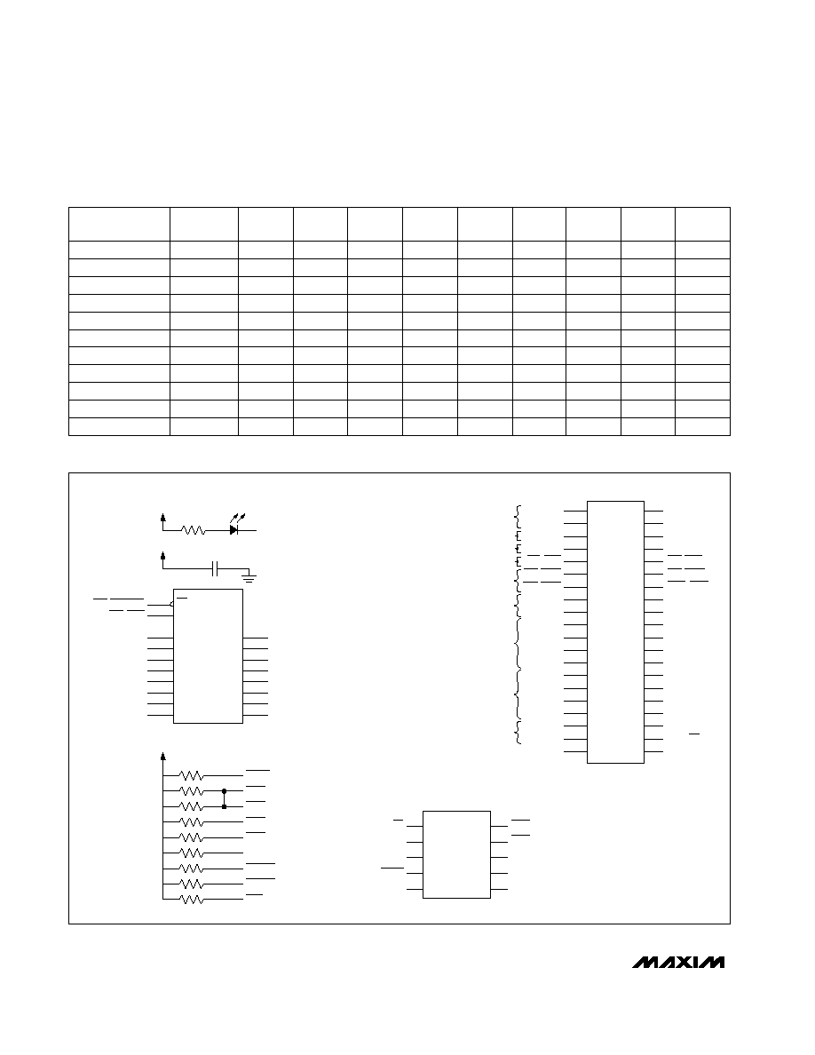
The 68HC16 uses a phase-locked loop (PLL) to set its
bus speed. Crystal Y1 is a 32.768kHz frequency refer-
ence. The internal oscillator runs 256 times faster than the
external crystal. When the 68HC16 is reset, it waits for the
PLL to lock before it executes any software. After the PLL
locks onto the reference frequency, the software doubles
the clock speed by writing to the clock synthesizer con-
trol register, selecting a bus speed of 16.78MHz.
U5, the user RAM area, is a 32kbyte CMOS static RAM.
The 74HCT245 octal buffer lets the 68HC16 module
access an 8-bit port on the 40-pin interface connector.
This memory-mapped port consists of separate read
and write strobes, four chip selects, four address LSBs,
and eight data bits.
Serial Communications
J3 is an RS-232 serial port, designed to be compatible
with the IBM PC 9-pin serial port. Use a straight-
through DB9 male-to-female cable to connect J3 to this
port. If the only available serial port has a 25-pin con-
nector, you may use a standard 25-pin to 9-pin
adapter. Table 1 shows the pinout of J3.
The MAX233 is an RS-232 interface voltage level shifter
with two transmitters and two receivers. It includes a
built-in charge pump with internal capacitors that gener-
ates the output voltages necessary to drive RS-232 lines.
40-Pin Data Connector J1
The 20 x 2 pin header connects the 68HC16 module to
a Maxim EV kit. Table 2 lists the function of each pin.
Note that 68HC16 object code is not compatible with
68HC11 object code. Use the 68HC16 module only
with those modules that are designed to support it, and
only download code that is targeted for the 68HC16
module. Downloading incorrect object code into the
68HC16 module will have unpredictable results.
Address Ranges
The 68HC16 µC generates various enable signals for dif-
ferent address ranges. The ROM and RAM enable sig-
nals are fed directly to the respective chips. Several
additional signals (J1.11≠J1.14) are available on the data
connector to be used by Maxim EV kits. Table 3 outlines
the address ranges for each of the elements found on
the 68HC16 module, and Table 4 is a truth table that
describes the logic for each of the 68HC16's chip-select
outputs. Because the addresses are not completely
decoded, the boot ROM and user RAM have shadows.
Unused
None
9
Handshake; hard-wired to RTS
CTS
8
Handshake; hard-wired to CTS
RTS
7
Handshake; hard-wired to DCD and DTR
DSR
6
Signal ground connection
GND
5
Handshake; hard-wired to DCD and DSR
DTR
4
RS-232-compatible data input to
68HC16 module
TXD
3
Handshake; hard-wired to DTR and DSR
DCD
1
FUNCTION
NAME
PIN
RS-232-compatible data output from
68HC16 module
RXD
2
Table 1. Serial Communications Port J3
Table 2. 40-Pin Data-Connector Signals
General I/O port bit 7
IC4
34
General I/O port bit 0 (LSB)
IC1
27
Buffered data bus bits 1≠7
EXTD1≠7
20≠26
Buffered data bus 0 (LSB)
EXTD0
19
Ground
GND
1≠4
FUNCTION
NAME
PIN
Unregulated input voltage
VPREREG
5, 6
Read strobe
RD
9
+5V from on-board regulator
VCC
7, 8
Chip select for 7E000≠7E7FF
7E000
11
Chip select for 7F000≠7F7FF
7F000
13
Write strobe
WR
10
Chip select for 7E800≠7EFFF
7E800
12
Address bit 0 (LSB)
A00
15
Chip select for 7F800≠7FFFF
7F800
14
Pulse-width-modulator output
PWMA
40
QSPI chip-select output
PCS0/SS
38
QSPI serial clock
SCK
37
QSPI master-out, slave-in
MOSI
36
QSPI master-in, slave-out
MISO
35
Address bit 1
A01
16
Address bit 2
A02
17
Address bit 3
A03
18
General I/O port bit 1
IC2
28
General I/O port bit 2
IC3
29
General I/O port bit 3
OC1
30
General I/O port bit 4
OC2
31
General I/O port bit 5
OC3
32
General I/O port bit 6
OC4
33
System clock output
CLKOUT
39
68HC16 Module
68HC16 Module
_______________________________________________________________________________________
3
Boot ROM
The boot ROM, U3, is configured as an 8-bit memory
device. Resistor R4 pulls data bit 0 low during system
reset, forcing the µC to fetch instructions using only the
upper eight data bits. The boot ROM checks the system
and waits for commands from the host. Refer to the EV
kit manual for specific start-up procedures.
Software
All software is supplied on a disk with the EV kit.
Instructions for operating the software are included in
the EV kit manual. Refer to the EV kit manual for more
information.
68HC16 Module Self Check
To test the 68HC16 module's integrity, connect the
power supply to the power terminals (J2). Do not con-
nect anything to J1 or J3. Slide the power switch SW1
to the "ON" position. The LED will light up, and will flash
within 5 seconds.
If the LED flashes with a 50%-on/50%-off duty cycle, then
it passed its self check. Note that this test does not exer-
cise the RS-232 port or the EV kit 40-pin interface, but it
does confirm that the power supply, microprocessor,
ROM, and RAM passed the self test.
If the LED flashes with a 10%-on/90%-off duty cycle,
then it failed its self check. Most likely, the RAM chip
(U5) is bad.
If the LED remains on and does not flash, then the prob-
lem is either U3 (the EPROM), U1 (the microprocessor),
U4 (the regulator), the MAX707 reset generator, or the
power supply. Use a voltmeter to verify that the power
supplies are good. Check the power-supply input and the
+5V output from the regulator. Use an oscilloscope to see
if the 32.768kHz reference oscillator is running.
Table 3. 68HC16 Module Memory Map
(all address values are in 20-bit hex)
Boot ROM (U3, strobed by CSBOOT)
00000≠07FFF
FUNCTION
PIN
Shadow of boot ROM
08000≠0FFFF
Shadow of user RAM
18000≠1FFFF
User RAM (U5, strobed by CS0 and CS2)
10000≠17FFF
Unused
20400≠7DFFF
Internal standby RAM; 1kbyte
20000≠203FF
Not accessed by the 68HC16
80000≠F7FFF
External chip select (J1 pin 11) (CS7)
7E000≠7E7FF
External chip select (J1 pin 12) (CS8)
7E800≠7EFFF
External chip select (J1 pin 13) (CS9)
7F000≠7F7FF
External chip select (J1 pin 14) (CS10)
7F800≠7FFFF
Unused
F8000≠FF6FF
68HC16's built-in ADC (not used)
FF700≠FF73F
Unused
FF740≠FF8FF
General-purpose timer module (GPT)
FF900≠FF93F
Unused
FF940≠FF9FF
System integration module (SIM)
FFA00≠FFA7F
Unused
FFA80≠FFAFF
Internal standby RAM (SRAM)
control registers
FFB00≠FFB07
Unused
FFB08≠FFBFF
Queued serial module (QSM)
FFC00≠FFDFF
Unused
FFE00≠FFFFF
68HC16 Module
68HC16 Module
4
_______________________________________________________________________________________
Table 4. 68HC16 Chip-Select Outputs Truth Table
H
1xxxx read
H
7E0xx read
H
1xxxx write
H
7E8xx read
H
7E0xx write
L
0xxxx read
CSBOOT
ADDRESS
RANGE
H
7F0xx write
H
7F8xx write
H
7F8xx read
H
7F0xx read
H
7E8xx write
H
H
L
H
H
H
H
H
H
H
H
CS0
H
L
H
L
H
H
H
L
L
H
L
H
H
H
H
CS1
H
H
H
H
H
H
H
CS2
H
H
H
H
L
L
L
H
H
L
H
L
H
H
L
CS5
L
L
L
L
L
L
H
CS6
H
L
H
H
L
H
H
H
H
H
H
H
H
H
L
CS7
H
H
H
H
H
L
H
CS8
H
H
H
H
H
L
H
H
L
H
H
CS9
H
H
H
H
H
H
L
L
H
H
H
CS10
19
1
2
3
4
5
6
7
8
9
CS6/IOBUFFER
CS1/RDIO
D08
D09
D10
D11
D12
D13
D14
D15
18
17
16
15
14
13
12
11
EXTD0
EXTD1
EXTD2
EXTD3
EXTD4
EXTD5
EXTD6
EXTD7
C13
0.1
µF
R5
470
LED1
GND
PWMB
VCC
VCC
VCC
TSTME
BKPT/DSCLK
BKPT/DSCLK
HALT
BERR
MODCLK
DSACK1
DSACK0
IRQ7
2
3
4
5
6
7
8
9
10
R6
10k
SIP
RESISTOR
1
DS
GND
GND
RESET
VCC
J4-1
J4-3
J4-5
J4-7
J4-9
J4-2
J4-4
J4-6
J4-8
J4-10
BERR
BKPT/DSCLK
FREEZE
IPIPE1/DSI
IPIPE0/DS0
OE
DIR
A1
A2
A3
A4
A5
A6
A7
A8
B1
B2
B3
B4
B5
B6
B7
B8
U6
74HCT245
J1-1
J1-3
J1-5
J1-7
J1-9
J1-11
J1-13
J1-15
J1-17
J1-19
J1-21
J1-23
J1-25
J1-27
J1-29
J1-31
J1-33
J1-35
J1-37
J1-39
J1-2
J1-4
J1-6
J1-8
J1-10
J1-12
J1-14
J1-16
J1-18
J1-20
J1-22
J1-24
J1-26
J1-28
J1-30
J1-32
J1-34
J1-36
J1-38
J1-40
GND
GND
VPREREG
VCC
CS1/RDIO
CS7/7E000
CS9/7F000
A00
A02
EXTD0
EXTD2
EXTD4
EXTD6
IC1
IC3
OC2
OC4
MISO
SCK
CLKOUT
GND
GND
VPREREG
VCC
CS5/WRIO
CS8/7E800
CS10/7F800
A01
A03
EXTD1
EXTD3
EXTD5
EXTD7
IC2
OC1
OC3
IC4
MOSI
PCSO/SS
PWMA
GROUND
UNREGULATED 7V TO 20V
REGULATED +5V
INTEL COMPATIBLE READ/WRITE STROBES
CHIP SELECTS
LOW ADDRESS BITS
8-BIT BUFFERED BIDIRECTIONAL DATA BUS
8-BIT GENERAL I/O PORT
HIGH-SPEED SERIAL INTERFACE (QSM/QSPI)
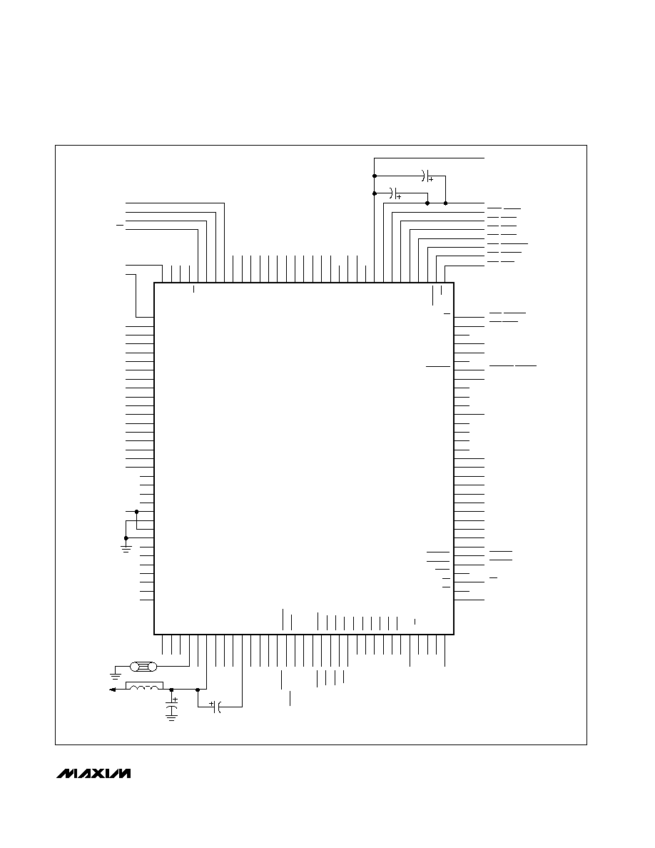
Figure 1. 68HC16 Module Schematic
68HC16 Module
68HC16 Module
_______________________________________________________________________________________
5
BR
FC2
FC1
VDDE
VSSE
FCO
CSBOOT
DATA0
DATA1
DATA2
DATA3
VSSI
DATA4
DATA5
DATA6
DATA7
DATA8
DATA9
VDDE
VSSE
DATA10
DATA11
DATA12
DATA13
DATA14
DATA15
ADDRO
DSACK0
DSACK1
AVEC
DS
AS
VDDE
A01
A02
VCC
VSSE
A03
A04
A05
A06
A07
A08
VSSI
A09
A10
A11
A12
A13
A14
VCC
VSSE
116
115
114
113
112
111
110
109
108
107
106
105
104
103
102
101
100
99
98
97
96
95
94
93
92
91
90
89
88
87
86
85
84
VRL
ADA6
ADA7
VSTBY
XTAL
VDDSYN
EXTAL
VSSI
VDDI
XFC
VDDE
VSSE
CLKOUT
FREEZE/QUOT
TSTME/TSC
BKPT/DSCLK
IPIPE0/DS0
IPIPE1/DS1
RESET
HALT
BERR
IRQ7
IRQ6
IRQ5
IRQ4
IRQ3
IRQ2
IRQ1
MODCLK
R/W
SIZ1
SIZ0
VSSE
51
52
53
54
55
56
57
58
59
60
61
62
63
64
65
66
67
68
69
70
71
72
73
74
75
76
77
78
79
80
81
82
83
18
19
20
21
22
23
24
25
26
27
28
29
30
31
32
33
34
35
36
37
38
39
40
41
42
43
44
45
46
47
48
49
50
TXD
ADDR1
ADDR2
VDDE
VSSE
ADDR3
ADDR4
ADDR5
ADDR6
ADDR7
ADDR8
VSSI
ADDR9
ADDR10
ADDR11
ADDR12
ADDR13
ADDR14
ADDR15
ADDR16
ADDR17
ADDR18
VDDE
VSSE
VDDA
VSSA
ADA0
ADA1
ADA2
ADA3
ADA4
ADA5
VRH
RXD
PCS3
PCS2
PCS1
PCS0/SS
SCK
MOSI
MISO
VSSE
VDDE
IC1
IC2
IC3
OC1
OC2
VSSI
VDDI
OC3
OC4
IC4/OC5
PAI
PWMA
PWMB
PCLK
VSSE
VDDE
ADDR23
ADDR22
ADDR21
ADDR20
ADDR19
BGACK
BG
17
16
15
14
13
12
11
10
9
8
7
6
5
4
3
2
1
132
131
130
129
128
127
126
125
124
123
122
121
120
119
118
117
CSO/WRRAM
CS5/WRIO
VCC
VSSE
CSBOOT/RDROM
DOO
VSSI
DO8
DO9
VCC
VSSE
D10
D11
D12
D13
D14
D15
AOO
DSACKO
DSACK1
DS
VCC
RXD
TXD
VCC
CS10/7F800
CS9/7F000
CS8/7E800
CS7/7E000
CS6/IOBUFFER
CS2/RDRAM
CS1/RDIO
VSSE
VCC
IC1
IC2
IC3
OC1
OC2
VSSI
VDDI
OC3
OC4
IC4
PWMA
PWMB
VSSE
MISO
MOSI
SCK
PCSO/SS
XTAL
EXTAL
VSSI
VDDI
VCC
VSSE
CLKOUT
FREEZE
TSTME
BKPT/DSCLK
IPIPEO/DS0
IPIPE1/DSI
RESET
HALT
BERR
IRQ7
MODCLK
VSSE
1
1
2
2
1
2
VCC
VSSE
VSTBY
L2
10
µH
OPTIONAL
C3
1
µF
20V
VSSI
C10
0.1
µF
C14
0.1
µF
C8
0.01
µF
U1
MOTOROLA
MC68HC16Z1CFC16
JU4
Figure 1. 68HC16 Module Schematic (continued)