Burr Brown Products
from Texas Instruments
FEATURES
APPLICATIONS
DESCRIPTION
ADS8413
SLAS490 ≠ OCTOBER 2005
16-BIT, 2-MSPS, LVDS SERIAL INTERFACE,
SAR ANALOG-TO-DIGITAL CONVERTER
∑
Medical Instrumentation
∑
2-MHz Sample Rate
∑
HIgh-Speed Data Acquisiton Systems
∑
16-Bit Resolution
∑
High-Speed Close-Loop Systems
∑
SNR 92 dB at 10 kHz I/P
∑
Communication
∑
THD ≠107 dB at 10 kHz I/P
∑
±
1 LSB Typ,
±
2 LSB INL Max
∑
+0.7/≠0.5 LSB Typ, +1.5/≠1 LSB DNL Max
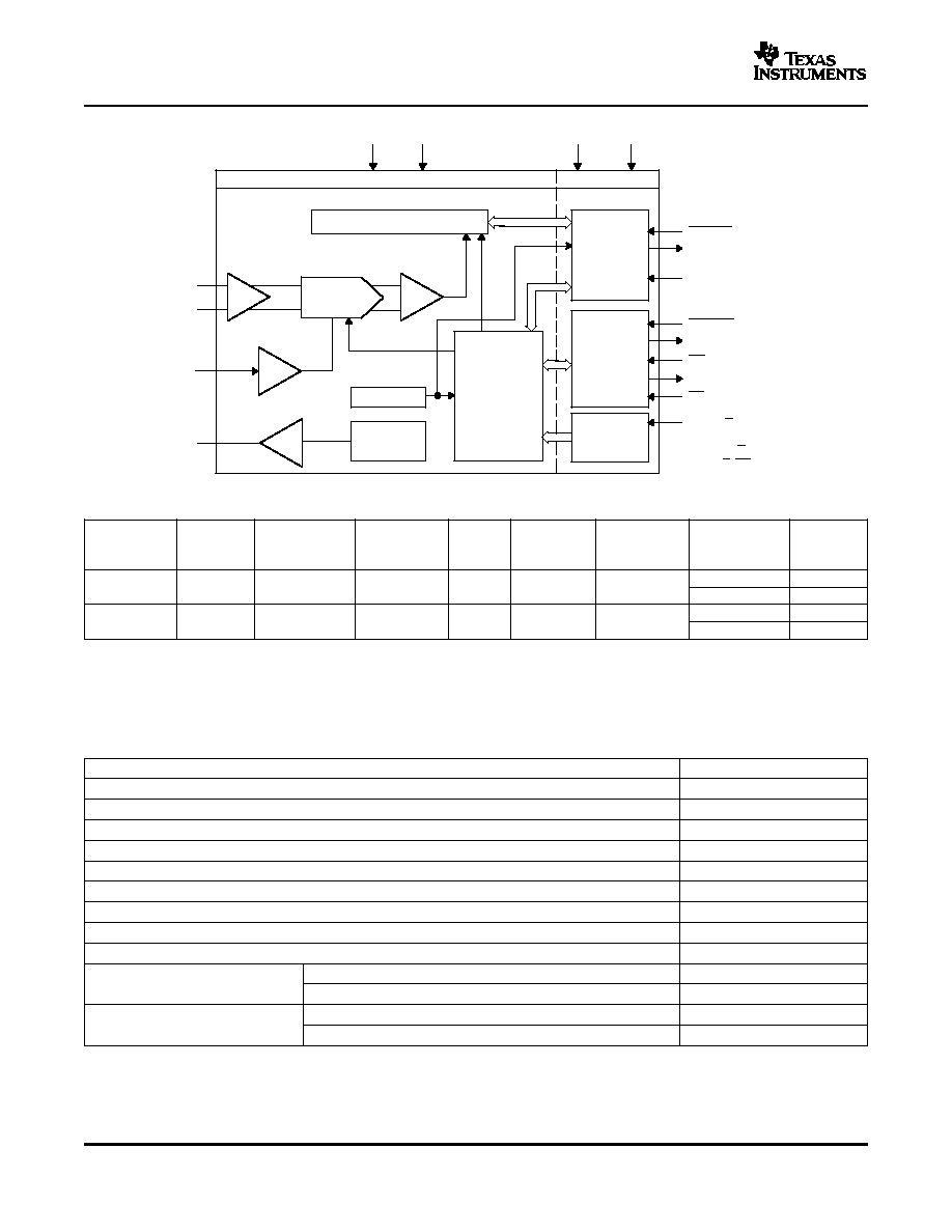
The ADS8413 is a 16-bit, 2-MSPS, analog-to-digital
∑
Unipolar Differential Input Range: ≠4 V
(A/D) converter with 4-V internal reference. The
to 4 V
device includes a capacitor based SAR A/D converter
∑
Internal Reference
with inherent sample and hold.
∑
Internal Reference Buffer
The ADS8413 also includes a 200-Mbps, LVDS,
serial interface. This interface is designed to support
∑
200-Mbps LVDS Serial Interface
daisy chaining or cascading of multiple devices. A
∑
Optional 200-MHz Internal Interface Clock
selectable 16-/8-bit data frame mode enables the use
∑
16-/8-Bit Data Frame
of a single shift register chip (SN65LVDS152) for
∑
Zero Latency at Full Speed
converting the data to parallel format.
∑
Power Dissipation: 290 mW at 2 MSPS
The
ADS8413
unipolar
differential
input
range
supports a differential input swing of ≠V
ref
to +V
ref
with
∑
Nap Mode (125 mW Power Dissipation)
a common-mode voltage of +V
ref
/2.
∑
Power Down (5
µ
W)
The nap feature provides substantial power saving
∑
48-Pin QFN Package
when used at lower conversion rates.
The ADS8413 is available in a 48-pin QFN package.
High-Speed SAR Converter Family
Type/Speed
500 kHz
~ 600 kHz
750 kHZ
1 MHz
1.25 MHz
2 MHz
3 MHz
4 MHz
ADS8383
ADS8381
18-Bit Pseudo-Diff
ADS8380 (S)
18-Bit Pseudo-Bipolar, Fully Diff
ADS8382 (S)
ADS8411
16-Bit Pseudo-Diff
ADS8370 (S)
ADS8371
ADS8401/05
ADS8410
(S-LVDS)
ADS8412
16-Bit Pseudo-Bipolar, Fully Diff
ADS8372 (S)
ADS8402/06
ADS8413
(S-LVDS)
14-Bit Pseudo-Diff
ADS7890 (S)
ADS7891
12-Bit Pseudo-Diff
ADS7881
Please be aware that an important notice concerning availability, standard warranty, and use in critical applications of Texas
Instruments semiconductor products and disclaimers thereto appears at the end of this data sheet.
PRODUCTION DATA information is current as of publication date.
Copyright © 2005, Texas Instruments Incorporated
Products conform to specifications per the terms of the Texas
Instruments standard warranty. Production processing does not
necessarily include testing of all parameters.
www.ti.com
CSTART
+ IN
CDAC
Core Supply
I/O Supply
SAR
LVDS I/O
CMOS I/O
Mode
Selection
Conversion
and
Control Logic
Clock
Comparator
4 V Internal
Reference
+
-
+ VA
AGND
+ VBD
BDGND
SYNC_O, CLK_O, SDO
SYNC_I, CLK_I, SDI
CONVST
BUS BUSY
RD
BUSY
CS
LAT_Y/N
BYTE,
MODE_C/D,
CLK_I/E, PD, NAP
- IN
REFIN
REFOUT
ABSOLUTE MAXIMUM RATINGS
ADS8413
SLAS490 ≠ OCTOBER 2005
ORDERING INFORMATION
(1)
MAXIMUM
MAXIMUM
NO MISSING
TRANSPORT
INTEGRAL
DIFFERENTIAL
CODES AT
PACKAGE
PACKAGE
TEMPERATURE
ORDERING
MODEL
MEDIA
LINEARITY
LINEARITY
RESOLUTION
TYPE
DESIGNATOR
RANGE
INFORMATION
QUANTITY
(LSB)
(LSB)
(BIT)
ADS8413IBRGZT
250
48 pin
≠40
∞
C
ADS8413lB
±
2
1.5/≠1
16
RGZ
QFN
to 85
∞
C
ADS8413IBRGZR
2000
ADS8413IRGZT
250
48 pin
≠40
∞
C
ADS8413l
±
4
3/≠1
16
RGZ
QFN
to 85
∞
C
ADS8413IRGZR
2000
(1)
For the most current package and ordering information, see the Package Option Addendum at the end of this document, or see the TI
website at
www.ti.com.
over operating free-air temperature range (unless otherwise noted)
(1)
UNIT
+IN to AGND
≠0.3 V to +VA + 0.3 V
-IN to AGND
≠0.3 V to +VA + 0.3 V
+VA to AGND
≠0.3 to 7 V
+VBD to BDGND
≠0.3 to 7 V
Digital input voltage to GND
≠0.3 V to (+VBD + 0.3 V)
Digital output to GND
≠0.3 V to (+VBD + 0.3 V)
Operating temperature range
≠40
∞
C to 85
∞
C
Storage temperature range
≠65
∞
C to 150
∞
C
Junction temperature (T
J
max)
150
∞
C
Power dissipation
(T
J
Max ≠ T
A
)/
JA
QFN package
JA
Thermal impedance
86
∞
C/W
Vapor phase (60 sec)
215
∞
C
Lead temperature, soldering
Infrared (15 sec)
220
∞
C
(1)
Stresses beyond those listed under absolute maximum ratings may cause permanent damage to the device. These are stress ratings
only, and functional operation of the device at these or any other conditions beyond those indicated under recommended operating
conditions is not implied. Exposure to absolute-maximum-rated conditions for extended periods may affect device reliability.
2
www.ti.com
SPECIFICATIONS
ADS8413
SLAS490 ≠ OCTOBER 2005
T
A
= ≠40
∞
C to 85
∞
C, +VA = 5 V,+VBD = 5 V or 3.3 V, V
ref
= 4.096 V, f
sample
= 2 MHz (unless otherwise noted)
PARAMETER
TEST CONDITIONS
MIN
TYP
MAX
UNIT
ANALOG INPUT
Full-scale input voltage span
(1)
+IN ≠ (≠IN)
≠V
ref
V
ref
V
+IN
≠0.2
V
ref
+ 0.2
Absolute input voltage range
V
≠IN
≠0.2
V
ref
+ 0.2
Input common-mode voltage range
V
ref
/2≠0.2
V
ref
/2
V
ref
/2+0.2
V
C
i
Input capacitance
25
pF
Input leakage current
500
pA
SYSTEM PERFORMANCE
Resolution
16
Bits
ADS8413IB
16
No missing codes
Bits
ADS8413I
16
ADS8413IB
≠2
±
1
2
INL
Integral linearity
(2)
LSB
(3)
ADS8413I
≠4.0
±
2
4.0
ADS8413IB
≠1
0.7/≠0.5
1.5
DNL
Differential linearity
LSB
(3)
ADS8413I
≠1.0
1.5/≠0.8
3
ADS8413IB
≠1
±
0.2
1
E
O
Offset error
External reference
mV
ADS8413I
≠3.0
±
1
3.0
ADS8413IB
≠0.1
±
0.03
0.1
E
G
Gain error
(4)
External reference
% of FS
ADS8413I
≠0.15
±
0.1
0.15
With common mode input signal = 200
CMMR
Common-mode rejection ratio
60
dB
mV
p-p
at 1 MHz
PSRR
Power supply rejection ratio
At FFF0
H
output code
80
dB
SAMPLING DYNAMICS
+VBD = 5 V
360
391
Conversion time
ns
+VBD = 3 V
391
+VBD = 5 V
100
Acquisition time
ns
+VBD = 3 V
100
Maximum throughput rate with or without latency
2.0
MHz
Aperture delay
20
ns
Aperture jitter
10
psec
Step response
50
ns
Overvoltage recovery
50
ns
DYNAMIC CHARACTERISTICS
V
IN
0.5 dB below FS at 10 kHz
≠107
THD
Total harmonic distortion
(5)
V
IN
0.5 dB below FS at 100 kHz
≠95
dB
V
IN
0.5 dB below FS at 0.5 MHz
≠90
V
IN
0.5 dB below FS at 10 kHz
92
SNR
Signal-to-noise ratio
V
IN
0.5 dB below FS at 100 kHz
90
dB
V
IN
0.5 dB below FS at 0.5 MHz
89
V
IN
0.5 dB below FS at 10 kHz
92
SINAD
Signal-to-noise and distortion
V
IN
0.5 dB below FS at 100 kHz
86
dB
V
IN
0.5 dB below FS at 0.5 MHz
84
V
IN
0.5 dB below FS at 10 kHz
≠113
SFDR
Spurious free dynamic range
V
IN
0.5 dB below FS at 100 kHz
≠98
dB
V
IN
0.5 dB below FS at 0.5 MHz
≠93
≠3 dB Small signal bandwidth
37.5
MHz
(1)
Ideal input span; does not include gain or offset error.
(2)
This is endpoint INL, not best fit.
(3)
Least significant bit
(4)
Measured relative to actual measured reference.
(5)
Calculated on the first nine harmonics of the input frequency.
3
www.ti.com
ADS8413
SLAS490 ≠ OCTOBER 2005
SPECIFICATIONS (continued)
T
A
= ≠40
∞
C to 85
∞
C, +VA = 5 V,+VBD = 5 V or 3.3 V, V
ref
= 4.096 V, f
sample
= 2 MHz (unless otherwise noted)
PARAMETER
TEST CONDITIONS
MIN
TYP
MAX
UNIT
EXTERNAL REFERENCE INPUT
Input voltage range, V
REF
3.9
4.096
4.2
V
Resistance
(6)
To internal reference voltage
500
k
INTERNAL REFERENCE OUTPUT
From 95% (+VA), with 1-
µ
F storage
25
Start-up time
ms
capacitor on REFOUT to AGND
Reference voltage range, V
ref
At room temperature
4.080
4.096
4.112
V
Source current
Static load
10
µ
A
Line regulation
+VA = 4.75 V to 5.25 V
0.6
mV
Drift
IOUT = 0 V
36
PPM/
∞
C
POWER SUPPLY REQUIREMENTS
+VBD
2.7
3.3
5.25
Power supply voltage
V
+VA
4.75
5
5.25
Supply current, 2-MHz sample rate +VA
58
64
mA
Power dissipation, 2-MHz sample rate
+VA = 5 V
290
320
mW
NAP MODE
Supply current
+VA
25
mA
POWER DOWN
Supply current
+VA
1
2.5
µ
A
Powerdown time
10
µ
s
With 1-
µ
F storage capacitor on
Powerup time
25
ms
REFOUT to AGND
Invalid conversions after power up or reset
3
Numbers
TEMPERATURE RANGE
Operating free air
≠40
85
∞
C
LOGIC FAMILY CMOS
V
IH
High-level input voltage
I
IH
= 5
µ
A
+VBD ≠1
+VBD +0.3
V
V
IL
Low-level input voltage
I
IL
= 5
µ
A
≠0.3
0.8
V
V
OH
High-level output voltage
I
OH
= 2 TTL loads
+VBD ≠ 0.6
+VBD
V
V
OL
Low-level output voltage
I
OL
= 2 TTL loads
0
0.4
V
LOGIC FAMILY LVDS
(7)
DRIVER
Steady-state differential output voltage
|V
OD(SS)
|
247
340
454
magnitude
R
L
= 100
, See
Figure 52
,
Figure 53
mV
Change in steady-state differential output voltage
-50
50
|V
OD(SS)
|
magnitude between logic states
V
OC(SS)
Steady-state common-mode output voltage
1.125
1.2
1.375
V
Change in steady-state common-mode output
|V
OC(SS)
|
≠50
50
voltage between logic states
See
Figure 54
mV
Peak to peak change in common-mode output
V
OC(pp)
50
150
voltage
V
OY
or V
OZ
= 0 V
3
10
I
OS
Short circuit output current
mA
V
OD
= 0 V
3
10
I
OZ
High impedance output current
VO = 0 V or +VBD
≠5
5
µ
A
(6)
Can vary
±
20%
(7)
All min max values ensured by design.
4
www.ti.com
TIMING REQUIREMENTS
ADS8413
SLAS490 ≠ OCTOBER 2005
SPECIFICATIONS (continued)
T
A
= ≠40
∞
C to 85
∞
C, +VA = 5 V,+VBD = 5 V or 3.3 V, V
ref
= 4.096 V, f
sample
= 2 MHz (unless otherwise noted)
PARAMETER
TEST CONDITIONS
MIN
TYP
MAX
UNIT
RECEIVER
V
ITH+
Positive going differential voltage threshold
50
mV
V
ITH-
Negative going differential voltage threshold
≠50
V
IC
Common mode input voltage
0.2
1.2
2.2
V
C
I
Input capacitance
5
pF
T
A
= ≠40
∞
C to 85
∞
C, +VA = 5 V, +VBD = 5 V or 3.3 V (unless otherwise noted)
PARAMETER
MIN
TYP
MAX
UNIT
REF
SAMPLING AND CONVERSION RELATED
Figure 1
,
t
acq
Acquisition time
100
ns
Figure 2
Figure 1
,
t
cnv
Conversion time
391
ns
Figure 2
t
w1
Pulse duration, CONVST high
100
ns
Figure 1
Figure 1
,
t
w2
Pulse duration, CONVST low
40
ns
Figure 2
t
d1
Delay time, CONVST rising edge to sample start
5
ns
Figure 1
Figure 1
,
t
d2
Delay time, CONVST falling edge to conversion start
5
ns
Figure 2
+VBD = 3.3 V
14
Figure 1
,
t
d3
Delay time, CONVST falling edge to busy high
ns
Figure 2
+VBD = 5 V
13
+VBD = 3.3 V
8
Figure 1
,
t
d4
Delay time, conversion end to busy low
ns
Figure 2
+VBD = 5 V
7
Figure 1
,
t
w3
Pulse duration, CSTART high
100
ns
Table 2
Figure 1
,
t
w4
Pulse duration, CSTART low
45
ns
Figure 2
,
Table 2
Figure 1
,
t
d5
Delay time, CSTART rising edge to sample start
7.5
ns
Table 2
Figure 1
,
t
d6
Delay time, CSTART falling edge to conversion start
7.5
ns
Figure 2
,
Table 2
+VBD = 3.3 V
16.5
Figure 1
,
t
d7
Delay time, CSTART falling edge to busy high
ns
Figure 2
,
+VBD = 5 V
15.5
Table 2
I/O RELATED
t
d8
Delay time, RD falling edge while CS low to BUS_BUSY high
16
ns
Figure 5
+VBD = 3.3 V
29
Delay time, RD falling edge while CS low to SYNC_O and SDO out of
t
d9
ns
Figure 5
3-state condition (for device with LAT_Y/N pulled low)
+VBD = 5 V
28
Delay time, pre_conversion end (point A) to SYNC_O and SDO out of 3-state
t
d10
22
ns
Figure 6
condition
VBD = 3.3 V
8
t
d11
Delay time, pre_conversion end (point A) to BUS_BUSY high
ns
Figure 6
+VBD = 5 V
7
t
d12
Delay time, conversion phase end to SYNC_O high
6
9 + t
CLK
ns
Figure 6
+VBD = 3.3 V
5.5 + 4*t
CLK
8.5 + 5*t
CLK
t
d13
Delay time, RD falling edge while CS low to SYNC_O high
ns
Figure 5
+VBD = 5 V
5 + 4*t
CLK
8 + 5*t
CLK
t
w5
Pulse duration, RD low for device in no latency mode
5
ns
Figure 11
+VBD = 3.3 V
1.4
Figure 5
,
t
d14
Delay time, CLK_O rising edge to data valid
ns
Figure 6
+VBD = 5 V
1.3
+VBD = 3.3 V
4*t
CLK
≠ 6.5
4*t
CLK
≠ 3
Delay time, BUS_BUSY low to SYNC_O high in daisy chain mode
Figure 7
,
t
d15
ns
indicating receiving device to output the data
Figure 12
+VBD = 5 V
4*t
CLK
≠ 6
4*t
CLK
≠ 2.5
5