 | –≠–ª–µ–∫—Ç—Ä–æ–Ω–Ω—ã–π –∫–æ–º–ø–æ–Ω–µ–Ω—Ç: DG302CK | –°–∫–∞—á–∞—Ç—å:  PDF PDF  ZIP ZIP |

General Description
Maxim's DG300≠DG303 and DG300A≠DG303A CMOS
dual and quad analog switches combine low power
operation with fast switching times and superior DC and
AC switch characteristics. On-resistance is less than
50
and is essentially constant over the analog signal
range. Device specifications are ideal for battery-
powered circuitry.
These switches are available in a variety of formats as
outlined in the Pin Configurations section. The switch
control logic inputs are fully TTL and CMOS compati-
ble. Also featured are "break-before-make" switching
and low charge injection.
Maxim's DG300-DG303 and DG300A-DG303A families
are electrically compatible and pin compatible with the
original manufacturer's devices. All devices operate with
power supplies ranging from ±5V to ±18V. Single-sup-
ply operation is implemented by connecting V- to GND.
Applications
Portable Instruments
Low-Power Sample/Holds
Power-Supply Switching
Programmable Gain Ampliffiers
SPDT and DPDT Functions
Process Control and Telemetry
Features
o Monolithic Low-Power CMOS
o Latchup Proof Construction
o Fully Compatible 2nd Source
o Low On-Resistance, <50
o Fast Switching Time
o V+ to V- Analog Signal Range
o Single-Supply Capability
DG300(A)/DG301(A)/DG302(A)/DG303(A)
TTL Compatible CMOS Analog Switches
________________________________________________________________ Maxim Integrated Products
1
V+
D
2
N.C.
S
2
S
1
N.C.
D
1
N.C.
14
13
12
11
10
9
8
1
2
3
4
5
6
7
N.C.
IN
2
V-
GND
IN
1
N.C.
10
1
2
3
4
5
6
7
8
9
D
1
S
1
IN
1
N.C.
GND
1
0
LOGIC
ON
OFF
SWITCH
DUAL SPST DG300/DG300A
DUAL DPST DG302/DG302A
V+ (SUBSTRATE AND CASE)
V-
IN
2
S
2
D
2
V+
S
4
D
4
D
2
D
1
D
3
S
3
N.C.
S
2
IN
2
V-
GND
IN
1
S
1
DUAL SPDT DG303/DG303A
V+
S
4
D
4
D
2
D
1
D
3
S
3
N.C.
S
2
IN
2
V-
GND
IN
1
S
1
1
0
LOGIC
ON
OFF
SWITCH
V+
D
2
N.C.
S
2
S
1
N.C.
D
1
N.C.
N.C.
N.C.
V-
SWITCH STATES ARE FOR LOGIC "1" INPUTS (POSITIVE LOGIC).
GND
IN
N.C.
10
1
2
3
4
5
6
7
8
9
D1
S1
IN
N.C.
GND
1
0
LOGIC
ON
OFF
SWITCH 1
OFF
ON
SWITCH 2
SPDT DG301/DG301A
V+ (SUBSTRATE AND CASE)
V-
N.C.
S2
D2
1
0
LOGIC
ON
OFF
SWITCHES 1, 3
OFF
ON
SWITCHES 2, 4
14
13
12
11
10
9
8
1
2
3
4
5
6
7
14
13
12
11
10
9
8
1
2
3
4
5
6
7
14
13
12
11
10
9
8
1
2
3
4
5
6
7
Pin Configurations
Ordering Information
19-0309; Rev 1; 6/99
For pricing, delivery, and ordering information, please contact Maxim/Dallas Direct! at
1-888-629-4642, or visit Maxim's website at www.maxim-ic.com.
Ordering Information continued at end of data sheet.
PART
TEMP RANGE
PIN-PACKAGE
DG300C/D
0∞C to +70∞C
Dice
DG300CJ
0∞C to +70∞C
14 Lead Plastic DIP
DG300CWE
0∞C to +70∞C
16 Lead Wide SO
DG300CK
0∞C to +70∞C
14 Lead CERDIP
DG300BWE
-25∞C to +85∞C
16 Lead Wide SO
DG300BK
-25∞C to +85∞C
14 Lead CERDIP
DG300BA
-25∞C to +85∞C
10 Lead Metal Can
DG300AK
-55∞C to +125∞C
14 Lead CERDIP
DG300AA
-55∞C to +125∞C
10 Lead Metal Can

DG300(A)/DG301(A)/DG302(A)/DG303(A)
TTL Compatible CMOS Analog Switches
2
_______________________________________________________________________________________
ABSOLUTE MAXIMUM RATINGS
ELECTRICAL CHARACTERISTICS
(V+ = +15V, V- = -15V, GND = 0V, T
A
= +25∞C, unless otherwise noted.)
Stresses beyond those listed under "Absolute Maximum Ratings" may cause permanent damage to the device. These are stress ratings only, and functional
operation of the device at these or any other conditions beyond those indicated in the operational sections of the specifications is not implied. Exposure to
absolute maximum rating conditions for extended periods may affect device reliability.
Voltages Referenced to V-
V+ (DG300≠DG303)...............................................................36V
V+ (DG300A≠DG303A) ..........................................................44V
GND .......................................................................................25V
Digital Inputs, V
S
, V
D
, (Note 1).......................-4V to (V+ + 4V) or
30mA, whichever occurs first
Current, Any Terminal Except S or D ..................................30mA
Continuous Current, S or D .................................................30mA
(pulsed at 1ms, 10% duty cycle max) ..........................100mA
Storage Temperature (A & B suffix)...................-65∞C to +150∞C
(C suffix) .........................-65∞C to +125∞C
Operating Temperature (A suffix) ......................-55∞C to +125∞C
(B suffix) ........................-25∞C to +85∞C
(C suffix) ...........................0∞C to +70∞C
Lead Temperature (soldering 10s) ..................................+300∞C
Power Dissipation*
Cerdip (K) (derate 11mW/∞C above +75∞C) ....................825mW
Plastic DIP (J) (derate 6.5mW/∞C above +25∞C) .............470mW
Metal Can (A) (derate 6mW/∞C above +75∞C).................450mW
*Device mounted with all leads soldered or welded to PC board.
DG300≠DG303A
DG300A≠DG303AA
DG300≠DG303B/C
DG300A≠DG303AB/C
PARAMETER
SYMBOL
TEST CONDITIONS
MIN
(Note 2)
TYP
(Note 3)
MAX
MIN
(Note 2)
TYP
(Note 3)
MAX
UNITS
Analog Signal Range
V
ANALOG
I
S
= 10mA, V
IN
= 0.8V or 4.0V
-15
+15
-15
+15
V
I
S
= -10mA, V
D
= 10V
30
50
30
50
Drain-Source
ON-Resistance
R
DS(ON)
I
S
= -10mA, V
D
= -10V
30
50
30
50
V
S
= 14V, V
D
= -14V
0.1
1
0.1
5
Source OFF-
Leakage Current
I
S(OFF)
V
S
= -14V, V
D
= 14V
-1
-0.1
-5
-0.1
nA
V
S
= -14V, V
D
= 14V
0.1
1
0.1
5
Drain OFF-
Leakage Current
I
D(OFF)
V
S
= 14V, V
D
= -14V
-1
-0.1
-5
-0.1
nA
V
D
= V
S
= 14V
0.1
2
0.1
5
SWITCH
Drain ON-
Leakage Current
I
D(ON)
V
IN
= 0.8V
or
V
IN
= 0.8V
V
D
= V
S
= -14V
-2
-0.1
-5
-0.1
nA
V
IN
= 5.0V
-1
-0.001
-1
-0.001
Input Current/
Voltage High
I
INH
V
IN
= 15V
0.001
1
0.001
1
µA
INPUT
Input Current/
Voltage Low
I
INL
V
IN
= 0V
-1
-0.001
-1
-0.001
µA
Turn-ON Time
t
ON
150
300
150
300
ns
Turn-OFF Time
t
OFF
See Switching Time Test Circuit
130
250
130
250
ns
Break-Before-Make
Interval
t
ON
- t
OFF
See Break-Before-Make Time Test
Circuit, DG301(A)/DG303(A) only
50
50
ns
Charge Injection
Q
C
L
= 10nF, R
GEN
= 0
, V
GEN
= 0V
12
12
pC
Source OFF-
Capacitance
C
S(OFF)
V
S
= 0V
14
14
pF
Drain OFF-
Capacitance
C
D(OFF)
V
D
= 0V
14
14
pF
Channel ON-
Capacitance
C
D(ON)
+
C
S(ON)
f = 1MHz,
V
IN
= 0.8V
or
V
IN
= 4.0V
V
S
= VD = 0V
40
40
pF
V
IN
= 0V
6
6
Input Capacitance
C
IN
f = 1MHz
V
IN
= 15V
7
7
pF
Off-Isolation (Note 4)
62
62
dB
DYNAMIC
Crosstalk
(Channel-to-Channel)
V
IN
= 0V, R
L
= 1k
V
S
= 1V
RMS
, f = 500kHz
74
74
dB

DG300(A)/DG301(A)/DG302(A)/DG303(A)
TTL Compatible CMOS Analog Switches
_______________________________________________________________________________________
3
ELECTRICAL CHARACTERISTICS (continued)
(V+ = +15V, V- = -15V, GND = 0V, T
A
= +25∞C, unless otherwise noted.)
DG300≠DG303A
DG300A≠DG303AA
DG300≠DG303B/C
DG300A≠DG303AB/C
PARAMETER
SYMBOL
TEST CONDITIONS
MIN
(Note 2)
TYP
(Note 3)
MAX
MIN
(Note 2)
TYP
(Note 3)
MAX
UNITS
Positive Supply
Current
I+
0.23
0.5
0.23
0.5
mA
Negative Supply
Current
I-
V
IN
= 4V (one input)
(all others = 0)
-10
-0.001
-10
-0.001
µA
Positive Supply
Current
I+
0.001
10
0.001
10
µA
SUPPLY
Negative Supply
Current
I-
V
IN
= 0.8V (all inputs)
-10
-0.001
-10
-0.001
µA
ELECTRICAL CHARACTERISTICS (Over Temperature)
(V+ = +15V, V- = -15V, GND = 0V, T
A
= Over Temperature Range, unless otherwise noted.)
DG300≠DG303A
DG300A≠DG303AA
DG300≠DG303B/C
DG300A≠DG303AB/C
PARAMETER
SYMBOL
TEST CONDITIONS
MIN
(Note 2)
TYP
(Note 3)
MAX
MIN
(Note 2)
TYP
(Note 3)
MAX
UNITS
Analog Signal Range
V
ANALOG
I
S
= -10mA, V
IN
= 0.8V or 4.0V
-15
+15
-15
+15
V
I
S
= -10mA, V
D
= 10V
75
75
Drain-Source
ON-Resistance
R
DS(ON)
I
S
= -10mA, V
D
= -10V
75
75
V
S
= 14V, V
D
= -14V
100
100
Source OFF-
Leakage Current
I
S(OFF)
V
S
= -14V, V
D
= 14V
-100
-100
nA
V
S
= -14V, V
D
= 14V
100
100
Drain OFF-
Leakage Current
I
D(OFF)
V
S
= 14V, V
D
= -14V
-100
-100
nA
V
D
= V
S
= 14V
200
200
SWITCH
Drain ON-
Leakage Current
I
D(ON)
V
IN
= 0.8V
or
V
IN
= 0.8V
V
D
= V
S
= -14V
-200
-200
nA
V
IN
= 5.0V
-1
-10
Input Current/
Voltage High
I
INH
V
IN
= 15V
1
10
µA
INPUT
Input Current/
Voltage Low
I
INL
V
IN
= 0V
-1
-10
µA
Positive Supply
Current
I+
1
1
mA
Negative Supply
Current
I-
V
IN
= 4V (one input)
(all others = 0)
-100
-200
mA
Positive Supply
Current
I+
100
200
µA
SUPPLY
Negative Supply
Current
I-
V
IN
= 0.8V (all inputs)
-100
-200
µA
Turn-ON Time
t
ON
500
ns
DYNAMIC
Turn-OFF Time
t
OFF
See Switching Time Test Circuit
450
ns

DG300(A)/DG301(A)/DG302(A)/DG303(A)
TTL Compatible CMOS Analog Switches
4
_______________________________________________________________________________________
ELECTRICAL CHARACTERISTICS (Over Temperature) (continued)
(V+ = +15V, V- = -15V, GND = 0V, T
A
= Over Temperature Range, unless otherwise noted.)
Note 1: Signals on S
X
, D
X
, or IN
X
exceeding V+ or V- are clamped by internal diodes. Limit diode forward current to maximum cur-
rent ratings.
Note 2: The algebraic convention whereby the most negative value is a minimum, and the most positive value is a maximum is used
in this data sheet.
Note 3: Typical values are for DESIGN AID ONLY, not guaranteed nor subject to production testing.
Note 4: OFF-isolation = 20 log V
S
, V
S
= input to OFF switch, V
D
= output.
V
D
Typical Operating Characteristics
(T
A
= +25∞C, unless otherwise noted.)
DG300(A)/DG301(A)/DG302(A)/DG303(A)
TTL Compatible CMOS Analog Switches
_______________________________________________________________________________________
5
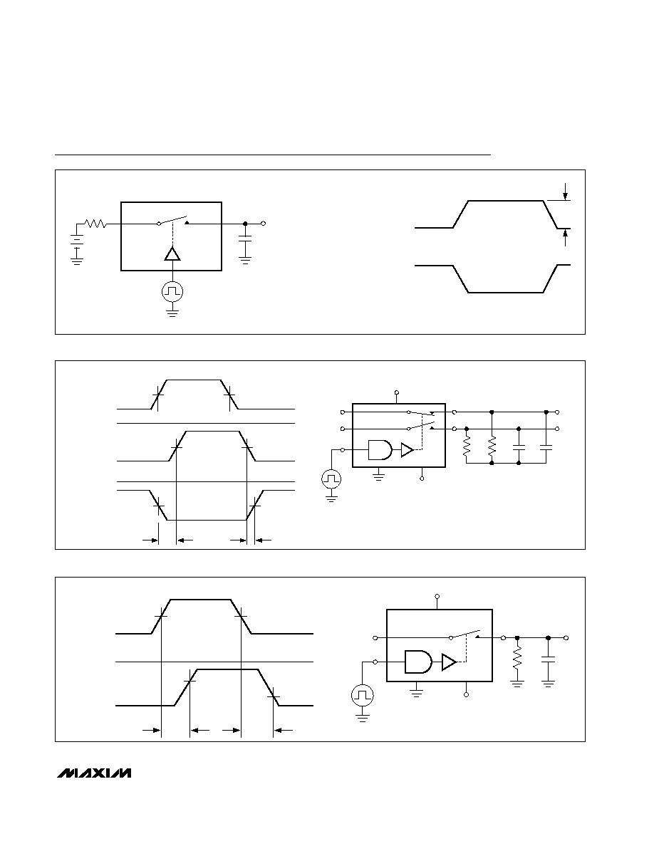
+15V
GND
V-
-15V
V+
IN
S
0
LOGIC
INPUT
V
O
SWITCH
OUTPUT
R
L
300
C
L
33pF
V
S
= 3V
LOGIC "1" = SWITCH ON
+4V
V
IHN
50%
LOGIC
INPUT
t
R
< 20ns
t
F
< 20ns
SWITCH
OUTPUT
0V
V
S
0V
90%
10%
t
ON
t
OFF
Figure 3. Switching Time Test Circuit
+15V
GND
V-
-15V
V+
IN
S
2
S
1
D
2
D
1
LOGIC
INPUT
V
O1
V
O2
SWITCH
OUTPUT
R
L2
300
R
L1
300
C
L2
33pF
C
L1
33pF
V
S1
= 3V
V
S2
= 3V
LOGIC "1" = SWITCH ON
+4V
V
IHN
50%
0V
50%
50%
LOGIC
INPUT
SWITCH
OUTPUT
SWITCH
OUTPUT
0V
0V
V
S2
V
S1
V
O1
V
O2
t
BBM
Figure 2. Break-Before-Make Time Test Circuit SPDT (DG301(A), DG303(A)
S
X
D
X
IN
X
R
GEN
V
GEN
V
O
C
L
10nF
V
O
ON
V
O
ON
IN
X
+4V
V
O
=
MEASURED VOLTAGE ERROR DUE TO CHARGE INJECTION
THE ERROR VOLTAGE IN COULOMBS IS
Q = C
L
x
V
O
.
0V
OFF
Figure 1. Charge Injection Test Circuit
Test Circuits