 | –≠–ª–µ–∫—Ç—Ä–æ–Ω–Ω—ã–π –∫–æ–º–ø–æ–Ω–µ–Ω—Ç: DG411CUE | –°–∫–∞—á–∞—Ç—å:  PDF PDF  ZIP ZIP |
_______________General Description
Maxim's redesigned DG411/DG412/DG413 analog
switches now feature low on-resistance matching
between switches (3
max) and guaranteed on-resis-
tance flatness over the signal range (
4 max). These
low on-resistance switches conduct equally well in
either direction. They guarantee low charge injection,
low power consumption, and an ESD tolerance of
2000V minimum per Method 3015.7. The new design
offers lower off leakage current over temperature (less
than 5nA at +85∞C).
The DG411/DG412/DG413 are quad, single-pole/sin-
gle-throw (SPST) analog switches. The DG411 is nor-
mally closed (NC), and the DG412 is normally open
(NO). The DG413 has two NC switches and two NO
switches. Switching times are less than 150ns max for
t
ON
and less than 100ns max for t
OFF
. These devices
operate from a single +10V to +30V supply, or bipolar
±4.5V to ±20V supplies. Maxim's improved
DG411/DG412/DG413 are fabricated with a 44V silicon-
gate process.
________________________Applications
Sample-and-Hold Circuits
Communication Systems
Test Equipment
Battery-Operated Systems
Heads-Up Displays
PBX, PABX
Guidance & Control Systems
Audio Signal Routing
Military Radios
______________________New Features
o Plug-In Upgrade for Industry-Standard
DG411/DG412/DG413
o Improved r
DS(ON)
Match Between Channels (3
max)
o Guaranteed r
FLAT(ON)
Over Signal Range (
4)
o Improved Charge Injection (10pC max)
o Improved Off Leakage Current Over Temperature
(<5nA at +85∞C)
o Withstand Electrostatic Discharge (2000V min)
per Method 3015.7
__________________Existing Features
o Low r
DS(ON)
(35
max)
o Single-Supply Operation +10V to +30V
o Bipolar-Supply Operation ±4.5V to ±20V
o Low Power Consumption (35µW max)
o Rail-to-Rail Signal Handling
o TTL/CMOS-Logic Compatible
______________Ordering Information
DG411/DG412/DG413
Improved, Quad,
SPST Analog Switches
________________________________________________________________ Maxim Integrated Products
1
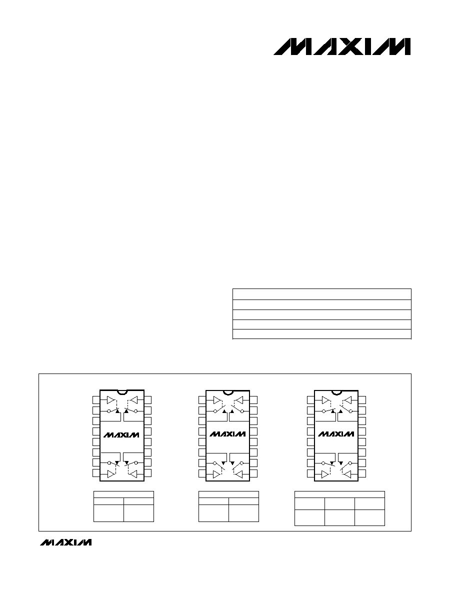
SWITCHES SHOWN FOR LOGIC "0" INPUT
DIP/SO/TSSOP
DG412
LOGIC
SWITCH
0
1
OFF
ON
TOP VIEW
DIP/SO/TSSOP
DG411
LOGIC
SWITCH
0
1
ON
OFF
DIP/SO/TSSOP
DG413
LOGIC
SWITCHES
1, 4
0
1
OFF
ON
SWITCHES
2, 3
ON
OFF
16
15
14
13
12
11
10
9
1
2
3
4
5
6
7
8
IN2
D2
S2
V+
V-
S1
D1
IN1
DG413
V
L
S3
D3
IN3
IN4
D4
S4
GND
16
15
14
13
12
11
10
9
1
2
3
4
5
6
7
8
IN2
D2
S2
V+
V-
S1
D1
IN1
DG411
V
L
S3
D3
IN3
IN4
D4
S4
GND
16
15
14
13
12
11
10
9
1
2
3
4
5
6
7
8
IN2
D2
S2
V+
V-
S1
D1
IN1
DG412
V
L
S3
D3
IN3
IN4
D4
S4
GND
_____________________Pin Configurations/Functional Diagrams/Truth Tables
19-4728; Rev 3; 9/99
Ordering Information continued at end of data sheet.
*Contact factory for dice specifications.
Dice*
0∞C to +70∞C
DG411C/D
16 Narrow SO
0∞C to +70∞C
DG411CY
16 Plastic DIP
0∞C to +70∞C
DG411CJ
PIN-PACKAGE
TEMP. RANGE
PART
16 TSSOP
0∞C to +70∞C
DG411CUE
For free samples & the latest literature: http://www.maxim-ic.com, or phone 1-800-998-8800.
For small orders, phone 1-800-835-8769.
DG411/DG412/DG413
Improved, Quad,
SPST Analog Switches
2
_______________________________________________________________________________________
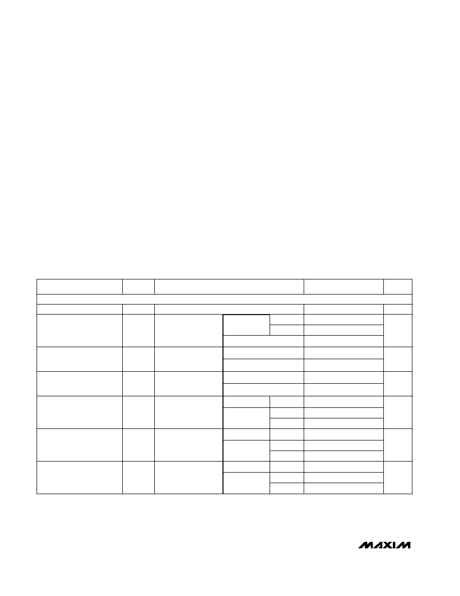
ABSOLUTE MAXIMUM RATINGS
ELECTRICAL CHARACTERISTICS--Dual Supplies
(V+ = 15V, V- = -15V, V
L
= 5V, GND = 0V, V
INH
= 2.4V, V
INL
= 0.8V, T
A
= T
MIN
to T
MAX
, unless otherwise noted.)
Stresses beyond those listed under "Absolute Maximum Ratings" may cause permanent damage to the device. These are stress ratings only, and functional
operation of the device at these or any other conditions beyond those indicated in the operational sections of the specifications is not implied. Exposure to
absolute maximum rating conditions for extended periods may affect device reliability.
Note 1: Signals on S, D, or IN exceeding V+ or V- are clamped by internal diodes. Limit forward current to maximum
current rating.
Voltage Referenced to V-
V+.........................................................................................44V
GND .....................................................................................25V
V
L
.....................................................(GND -0.3V) to (V+ +0.3V)
Digital Inputs, V
S
, V
D
(Note 1)........(V- -2V) to (V+ +2V) or 30mA
(whichever occurs first)
Continuous Current (any terminal) ......................................30mA
Peak Current
(pulsed at 1ms, 10% duty cycle max) ............................100mA
Continuous Power Dissipation (T
A
= +70∞C)
16-Pin Plastic DIP (derate 10.53mW/∞C above +70∞C) .842mW
16-Pin Narrow SO (derate 8.70mW/∞C above +70∞C) ...696mW
16-Pin CERDIP (derate 10.00mW/∞C above +70∞C)......800mW
16-Pin TSSOP (derate 6.7mW/∞C above +70∞C) ...........457mW
Operating Temperature Ranges
DG41_C_ ..............................................................0∞C to +70∞C
DG41_D_ ...........................................................-40∞C to +85∞C
DG41_AK_ .......................................................-55∞C to +125∞C
Storage Temperature Range .............................-65∞C to +150∞C
Lead Temperature (soldering, 10sec) .............................+300∞C
17
30
A
C, D
-40
40
-10
10
-10
10
-0.25
-0.10
0.25
6
5
A
A
A
T
A
= T
MIN
to T
MAX
T
A
= T
MIN
to T
MAX
C, D
C, D
C, D
T
A
= T
MIN
to T
MAX
T
A
= +25∞C
T
A
= T
MIN
to
T
MAX
T
A
= +25∞C
T
A
= T
MIN
to
T
MAX
T
A
= +25∞C
T
A
= T
MIN
to
T
MAX
T
A
= +25∞C
T
A
= +25∞C
T
A
= +25∞C
V+ = 16.5V,
V- = -16.5V,
V
D
= ±15.5V,
V
S
= 15.5V
V+ = 16.5V,
V- = -16.5V,
V
D
= ±15.5V,
V
S
= 15.5V
(Note 3)
V+ = 16.5V,
V- = -16.5V,
V
D
= ±15.5V,
V
S
= 15.5V
V+ = 15V, V- = -15V,
V
D
= ±10V,
I
S
= -10mA
V+ = 13.5V,
V- = -13.5V,
V
D
= ±8.5V,
I
S
= -10mA
V+ = 15V, V- = -15V,
V
D
= ±5V, 0V,
I
S
= -10mA
CONDITIONS
nA
-20
20
I
D(ON)
+
I
S(ON)
Drain-On Leakage Current
(Note 7)
-0.4
-0.1
0.4
I
D(OFF)
nA
-5
5
Drain-Off Leakage Current
(Note 7)
-5
5
nA
I
S(OFF)
Source-Off Leakage Current
(Note 7)
-0.25
-0.10
0.25
4
r
FLAT(ON)
On-Resistance Flatness
(Note 4)
V
-15
15
V
ANALOG
Analog Signal Range
r
DS(ON)
On-Resistance
Match Between Channels
(Note 4)
3
17
45
45
r
DS(ON)
Drain-Source
On-Resistance
UNITS
MIN
TYP
MAX
(Note 2)
SYMBOL
PARAMETER
C, D, A
C, D, A
C, D, A
SWITCH
±
±
±

IN = 2.4V, all others = 0.8V
DG411/DG412/DG413
Improved, Quad,
SPST Analog Switches
_______________________________________________________________________________________
3
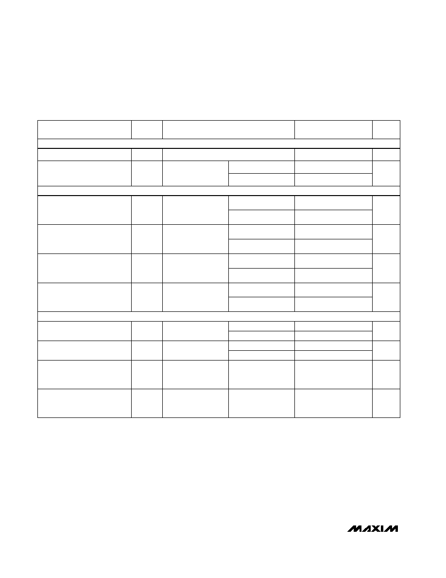
ELECTRICAL CHARACTERISTICS--Dual Supplies (continued)
(V+ = 15V, V- = -15V, V
L
= 5V, GND = 0V, V
INH
= 2.4V, V
INL
= 0.8V, T
A
= T
MIN
to T
MAX
, unless otherwise noted.)
ns
ns
-5
5
T
A
= T
MIN
to T
MAX
-5
5
T
A
= T
MIN
to T
MAX
T
A
= +25∞C
-5
5
T
A
= T
MIN
to T
MAX
-5
5
T
A
= T
MIN
to T
MAX
T
A
= +25∞C
T
A
= +25∞C
T
A
= +25∞C
T
A
= +25∞C
T
A
= +25∞C
T
A
= +25∞C
T
A
= +25∞C
T
A
= T
MIN
to T
MAX
T
A
= +25∞C
T
A
= T
MIN
to T
MAX
T
A
= +25∞C
T
A
= +25∞C
IN = 0.8V, all others = 2.4V
T
A
= +25∞C
CONDITIONS
T
A
= +25∞C
-1
-0.0001
1
All channels on or off,
V+ = 16.5V,
V- = -16.5V,
V
IN
= 0V or 5V
All channels on or off,
V+ = 16.5V,
V- = -16.5V,
V
IN
= 0V or 5V
All channels on or off,
V+ = 16.5V,
V- = -16.5V,
V
IN
= 0V or 5V
pF
35
f = 1MHz, Figure 8
C
D(ON)
+
C
S(ON)
Drain-On Capacitance
pF
9
f = 1MHz, Figure 7
C
D(OFF)
Drain-Off Capacitance
pF
9
f = 1MHz, Figure 7
C
S(OFF)
Source-Off Capacitance
dB
85
R
L
= 50
,
C
L
= 5pF,
f = 1MHz, Figure 6
Crosstalk (Note 6)
dB
68
R
L
= 50
,
C
L
= 5pF,
f = 1MHz, Figure 5
OIRR
Off Isolation (Note 5)
pC
5
10
C
L
= 1.0nF,
V
GEN
= 0V,
R
GEN
= 0
, Figure 4
Q
Charge Injection (Note 3)
ns
25
DG413 only,
R
L
= 300
,
C
L
= 35pF, Figure 3
t
D
Break-Before-Make Time Delay
V
D
= ±10V,
Figure 2
V
D
= ±10V,
Figure 2
160
t
OFF
Turn-Off Time
100
145
220
t
ON
Turn-On Time
µA
-0.500
0.005
0.500
I
INH
110
175
Input Current with Input Voltage
High
-1
-0.0001
1
µA
I
GND
Ground Current
µA
-1
0.0001
1
I
L
Logic Supply Current
µA
-1
0.0001
1
I+
Positive Supply Current
µA
µA
-0.500
0.005
0.500
I
INL
Input Current with Input Voltage
Low
All channels on or off,
V+ = 16.5V,
V- = -16.5V,
V
IN
= 0V or 5V
V
I-
Negative Supply Current
±4.5
±20.0
Power-Supply Range
UNITS
MIN
TYP
MAX
(Note 2)
SYMBOL
PARAMETER
INPUT
SUPPLY
DYNAMIC
DG411/DG412/DG413
Improved, Quad,
SPST Analog Switches
4
_______________________________________________________________________________________
ELECTRICAL CHARACTERISTICS--Single Supply
(V+ = 12V, V- = 0V, V
L
= 5V, GND = 0V, V
INH
= 2.4V, V
INL
= 0.8V, T
A
= T
MIN
to T
MAX
, unless otherwise noted.)
Note 2:
The algebraic convention, where the most negative value is a minimum and the most positive value a maximum, is used in
this data sheet.
Note 3:
Guaranteed by design.
Note 4:
R
ON
=
R
ON
max -
R
ON
min. On-resistance match between channels and flatness are guaranteed only with
bipolar-supply operation. Flatness is defined as the difference between the maximum and minimum value of on resistance
as measured at the extremes of the specified analog signal range.
Note 5:
Off Isolation = 20 log (V
D/
V
S)
, V
D
= output, V
S
= input to off switch. See Figure 5.
Note 6:
Between any two switches. See Figure 6.
Note 7:
Leakage parameters I
S(OFF)
, I
D(OFF)
, and I
D(ON)
are 100% tested at the maximum rated hot temperature and guaranteed
by correlation at +25∞C.
-5
5
T
A
= +25∞C
T
A
= T
MAX
-5
5
T
A
= T
MAX
-5
5
T
A
= T
MAX
315
T
A
= T
MIN
to T
MAX
-5
5
T
A
= T
MAX
T
A
= +25∞C
T
A
= +25∞C
T
A
= T
MIN
to T
MAX
T
A
= +25∞C
T
A
= +25∞C
T
A
= +25∞C
T
A
= +25∞C
T
A
= +25∞C
T
A
= +25∞C
T
A
= T
MIN
to T
MAX
CONDITIONS
pC
5
10
C
L
= 1.0nF,
V
GEN
= 0V,
R
GEN
= 0V,
Figure 4
Q
Charge Injection
(Note 3)
ns
25
DG413 only,
R
L
= 300
, C
L
= 35pF,
Figure 3
t
D
Break-Before-Make Time Delay
V
S
= 8V,
Figure 2
V
S
= 8V,
Figure 2
All channels on or off,
V
L
= 5.25V,
V
IN
= 0V or 5V
All channels on or off,
V+ = 13.2V,
V
IN
= 0V or 5V
All channels on or off,
V
L
= 5.25V,
V
IN
= 0V or 5V
All channels on or off,
V+ = 13.2V,
V
IN
= 0V or 5V
V+ = 10.8V,
V
D
= 3.8V,
I
S
= -10mA
ns
140
t
OFF
Turn-Off Time
40
80
95
125
t
ON
ns
175
250
V
0
12
V
ANALOG
Turn-On Time
µA
-1
-0.0001
1
I
GND
Analog Signal Range
Ground Current
µA
-1
0.0001
1
I-
Negative Supply Current
µA
-1
0.0001
1
I
L
µA
-1
0.0001
1
I+
Positive Supply Current
Logic Supply Current
100
r
DS(ON)
Drain-Source On Resistance
UNITS
MIN
TYP
MAX
(Note 2)
SYMBOL
PARAMETER
SWITCH
SUPPLY
DYNAMIC
(Note 3)

DG411/DG412/DG413
Improved, Quad,
SPST Analog Switches
_______________________________________________________________________________________
5
60
-20
-10
10
ON-RESISTANCE vs. V
D
AND
POWER-SUPPLY VOLTAGE
0
40
DG411-01
V
D
(V)
r
DS(ON)
()
0
20
20
50
30
10
70
A
B
C
D
A: V+ = 5V,
V- = -5V
B: V+ = 10V,
V- = -10V
C: V+ = 15V,
V- = -15V
D: V+ = 20V,
V- = -20V
0
-20
-10
10
ON-RESISTANCE vs. V
D
AND
TEMPERATURE
50
DG411-02
V
D
(V)
r
DS(ON)
()
0
20
30
10
40
20
60
V+ = 15V
V- = -15V
T
A
= +125∞C
T
A
= +85∞C
T
A
= +25∞C
T
A
= -55∞C
20
0
5
15
ON-RESISTANCE vs. V
D
AND
TEMPERATURE (SINGLE SUPPLY)
120
DG411-03
V
D
(V)
r
DS(ON)
()
10
20
80
40
100
60
140
V- = 0V
V+ = 5V
V+ = 10V
V+ = 15V
V+ = 20V
160
20
0
5
15
ON-RESISTANCE vs. V
D
(SINGLE SUPPLY)
70
DG411-04
V
D
(V)
r
DS(ON)
()
10
20
50
30
60
40
80
V+ = 12V
V- = 0V
T
A
= +125∞C
T
A
= +85∞C
T
A
= +25∞C
0.0001
-55
OFF LEAKAGE CURRENTS vs.
TEMPERATURE
10
DG411-05
TEMPERATURE (∞C)
OFF LEAKAGE (nA)
+25
+125
0.1
0.001
1
0.01
100
V+ = 16.5V
V- = -16.5V
V
D
= ±15V
V
S
= 15V
±
0.0001
-55
ON LEAKAGE CURRENTS vs.
TEMPERATURE
10
DG411-06
TEMPERATURE (∞C)
ON LEAKAGE (nA)
+25
+125
0.1
0.001
1
0.01
100
V+ = 16.5V
V- = -16.5V
V
D
= ±15V
V
S
= ±15V
__________________________________________Typical Operating Characteristics
(T
A
= +25∞C, unless otherwise noted.)
-60
-20
CHARGE INJECTION vs.
ANALOG VOLTAGE
40
DG411-07
V
D
(V)
Q (pC)
0
20
0
-40
20
-20
60
-15 -10
-5
5
10
15
V+ = 15V
V- = -15V
V
L
= 5V
CL = 1nF
0.0001
-55
SUPPLY CURRENT vs. TEMPERATURE
10
DG411-08
TEMPERATURE (∞C)
I+, I-, I
L
(
µ
A)
+25
+125
0.1
0.001
1
0.01
100
A: I+ at V+ = 16.5V
B: I- at V- = -16.5V
C: I
L
at V
L
= 5V
A
B
C