 | –≠–ª–µ–∫—Ç—Ä–æ–Ω–Ω—ã–π –∫–æ–º–ø–æ–Ω–µ–Ω—Ç: DG413FDY | –°–∫–∞—á–∞—Ç—å:  PDF PDF  ZIP ZIP |
General Description
The DG411F/DG412F/DG413F are quad, single-pole/sin-
gle-throw (SPST), fault-protected analog switches. They
are pin compatible with the industry-standard nonpro-
tected DG411/DG412/DG413. These new switches fea-
ture fault-protected inputs and Rail-to-Rail
signal-
handling capability. All terminals are protected from
overvoltage faults up to ±36V with power on and up to
±40V with power off. During a fault condition, the COM,
NO, or NC terminal becomes an open circuit and only
microamperes of leakage current flow from the source.
On-resistance is 35
(max) and is matched between
switches to 1.5
(max) at +25∞C.
The DG411F has four normally closed (NC) switches.
The DG412F has four normally open (NO) switches.
The DG413F has two NC and two NO switches. These
CMOS switches operate with dual power supplies rang-
ing from ±4.5V to ±20V or a single supply between +9V
and +36V. All digital inputs have +0.8V and +2.4V logic
thresholds, ensuring both TTL and CMOS logic com-
patibility when using ±15V or a single +12V supply.
For supply voltages of ±5V, +5V, and +3V, refer to the
MAX4711/MAX4712/MAX4713 data sheet.
Applications
Communication Systems
Signal Routing
Test Equipment
Data Acquisition
Industrial and Process Control Systems
Avionics
Redundant/Backup Systems
Features
o No Power-Supply Sequencing Required
o Rail-to-Rail Signal Handling
o All Switches Off with Power Off
o All Switches Off when V+ is Off and V- is On
o ±40V Fault Protection with Power Off
o ±36V Fault Protection with ±15V Supplies
o Control Line Fault Protection from
V- - 0.3V to V- + 40V
o Pin Compatible with Industry-Standard
DG411/DG412/DG413
o 20ns (typ) Fault Response Time
o 35 (max) R
ON
with ±15V Supplies
o ±4.5V to ±20V Dual Supplies
o +9V to +36V Single Supply
o TTL- and CMOS-Compatible Logic Inputs with
±15V or Single +9V to +15V Supplies
DG411F/DG412F/DG413F
Quad, Rail-to-Rail, Fault-Protected,
SPST Analog Switches
19-2418; Rev 0; 4/02
For pricing, delivery, and ordering information, please contact Maxim/Dallas Direct! at
1-888-629-4642, or visit Maxim's website at www.maxim-ic.com.
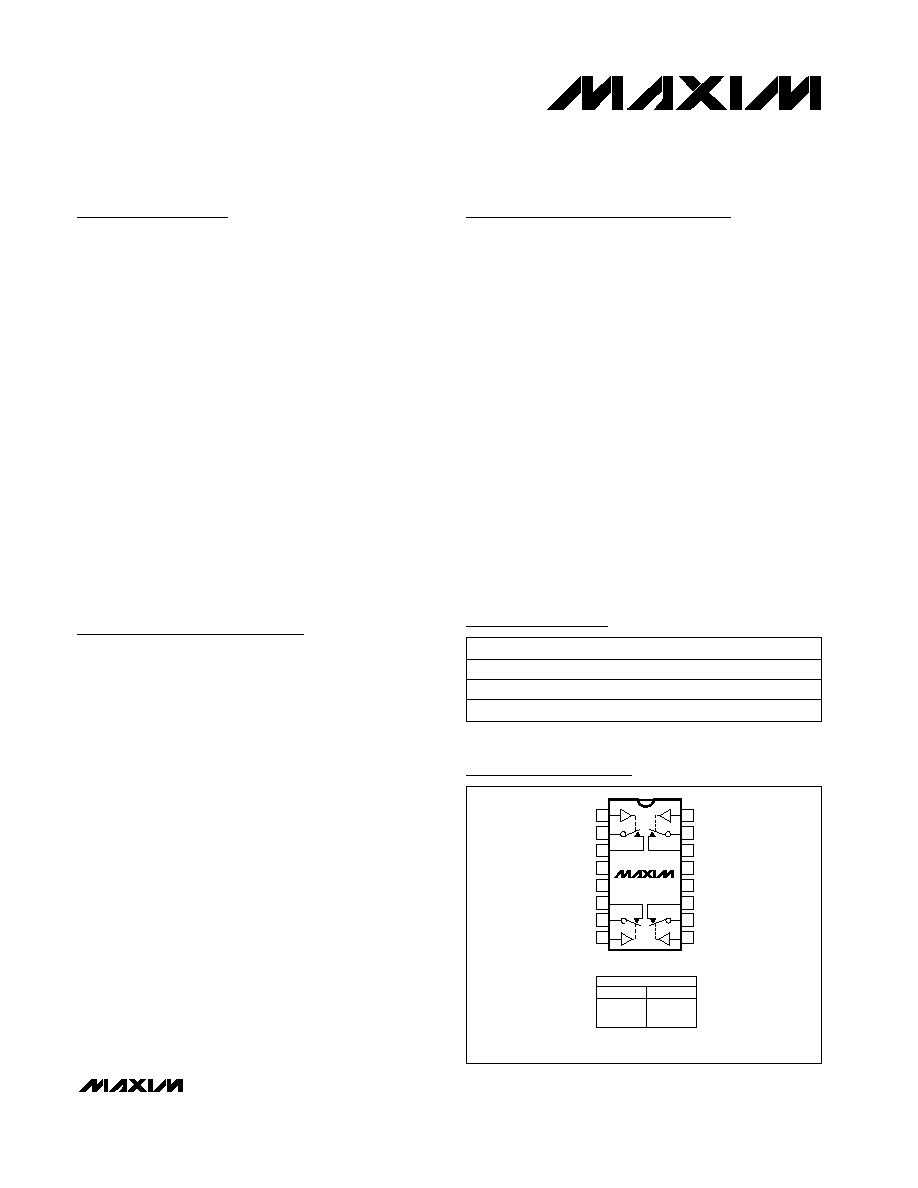
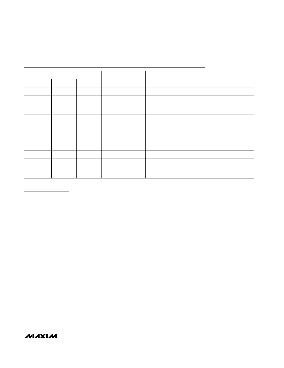
Ordering Information
PART
TEMP RANGE
PIN-PACKAGE
DG411FEUE
-40∞C to +85∞C
16 TSSOP
DG411FDY
-40∞C to +85∞C
16 SO
DG411FDJ
-40∞C to +85∞C
16 Plastic DIP
N.C. = NOT CONNECTED. SWITCHES SHOWN FOR LOGIC 0 INPUT.
ALL SWITCHES ARE OFF WITH POWER REMOVED.
TOP VIEW
DIP/TSSOP/SO
DG411F
LOGIC
SWITCH
0
1
ON
OFF
16
15
14
13
12
11
10
9
1
2
3
4
5
6
7
8
IN2
COM2
NC2
V+
V-
NC1
COM1
IN1
DG411F
N.C.
NC3
COM3
IN3
IN4
COM4
NC4
GND
Pin Configurations
________________________________________________________________ Maxim Integrated Products
1
Rail-to-Rail is a registered trademark of Nippon Motorola, Ltd.
Pin Configurations continued at end of data sheet.
Functional Diagram appears at end of data sheet.
Ordering Information continued at end of data sheet.
DG411F/DG412F/DG413F
Quad, Rail-to-Rail, Fault-Protected,
SPST Analog Switches
2
_______________________________________________________________________________________
ABSOLUTE MAXIMUM RATINGS
Stresses beyond those listed under "Absolute Maximum Ratings" may cause permanent damage to the device. These are stress ratings only, and functional
operation of the device at these or any other conditions beyond those indicated in the operational sections of the specifications is not implied. Exposure to
absolute maximum rating conditions for extended periods may affect device reliability.
(Voltages Referenced to GND)
V+ ...........................................................................-0.3V to +44V
V- ............................................................................-44V to +0.3V
V+ to V-...................................................................-0.3V to +44V
IN_ ......................................................... (V- - 0.3V) to (V- + 40V)
NO_, NC_ to COM_ (Note1) ................................... -40V to +40V
COM_, NO_, NC_ Voltage with
Power On (Note 1).............................................. -36V to +36V
COM_, NO_, NC_ Voltage with
Power Off (Note 1).............................................. -40V to +40V
Continuous Current (any terminal) ..................................
±30mA
Peak Current COM_, NO_, NC_
(pulsed at 1ms, 10% duty cycle) ...............................
±100mA
Continuous Power Dissipation (T
A
= +70∞C)
16-Pin TSSOP (derate 9.4mW/∞C above +70∞C) ....... 755mW
16-Pin SO (derate 8.7mW/∞C above +70∞C)................696mW
16-Pin Plastic DIP (derate 10.53mW/∞C
above +70∞C) ........................................................ 842mW
Operating Temperature Range .......................... -40∞C to +85∞C
Junction Temperature .................................................... +150∞C
Storage Temperature Range ........................... -65∞C to +160∞C
Lead Temperature (soldering, 10s) ............................... +300∞C
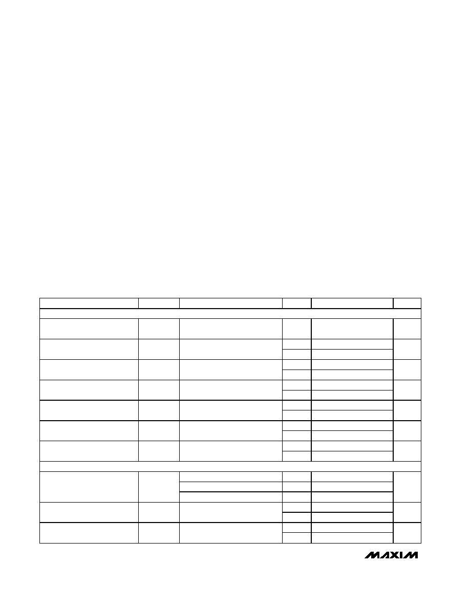
ELECTRICAL CHARACTERISTICS--
±15V Dual Supplies
(V+ = +15V, V- = -15V, V
IH
= +2.4V, V
IL
= +0.8V, GND = 0, T
A
= T
MIN
to T
MAX
, unless otherwise noted. Typical values are at
T
A
= +25
∞C.) (Notes 2, 3)
PARAMETER
SYM B O L
CONDITIONS
T
A
MIN
TYP
MAX
UNITS
ANALOG SWITCH
Fault-Free Analog Signal Range
V
C OM _
,
V
N O_
, V
N C _
E
V-
V+
V
+25∞C
25
35
On-Resistance
R
ON
I
COM_
= 10mA,
V
NO_
, V
NC_
=
±10V
E
45
+25∞C
0.2
1.5
On-Resistance Match Between
Channels (Note 4)
R
ON
I
COM_
= 10mA,
V
NO_
, V
NC_
=
±10V
E
2.0
+25∞C
1.0
3
On-Resistance Flatness
R
FLAT(ON)
I
COM_
= 10mA,
V
NO_
, V
NC_
=
±5V, 0
E
4
+25∞C
-0.25
+0.025
+0.25
NO_, NC_ Off-Leakage Current
(Note 5)
I
NO_(OFF)
,
I
NC_(OFF)
V
COM_
=
±10V,
V
NO_
, V
NC_
= > 10V
E
-20
+20
nA
+25∞C
-0.25
+0.025
+0.25
COM_ Off-Leakage Current
(Note 5)
I
COM_(OFF)
V
COM_
=
±10V,
V
NO_
, V
NC_
= > 10V
E
-20
+20
nA
+25∞C
-0.5
+0.025
+0.5
COM_ On-Leakage Current
(Note 5)
I
COM_(ON)
V
COM_
=
±10V,
V
NO_
, V
NC_
=
±10V or floating
E
-40
+40
nA
FAULT
V+ = +15V, V- = -15V
E
-36
+36
V+ = 0, V- = -15V
E
-36
+36
Fault-Protected Analog Signal
Range
V
COM_
,
V
NO_,
V
NC_
V+ = V- = 0
E
-40
+40
V
+25∞C
-1
+1
NO_ or NC_ Off-Leakage
Current
I
NO_
, I
NC_
V
NO_
, V
NC_
=
±36V
E
-10
+10
µA
+25∞C
-1
+1
COM_ Off-Leakage Current
I
COM_
V
COM_
=
±36V
E
-10
+10
µA
Note 1: COM_, NO_, and NC_ pins are fault protected. Signals on COM_, NO_, and NC_ exceeding -36V to +36V may damage the
device during power-on conditions. When the power is off, the maximum range is -40V to +40V.
DG411F/DG412F/DG413F
Quad, Rail-to-Rail, Fault-Protected,
SPST Analog Switches
_______________________________________________________________________________________
3
ELECTRICAL CHARACTERISTICS--
±15V Dual Supplies (continued)
(V+ = +15V, V- = -15V, V
IH
= +2.4V, V
IL
= +0.8V, GND = 0, T
A
= T
MIN
to T
MAX
, unless otherwise noted. Typical values are at
T
A
= +25
∞C.) (Notes 2, 3)
PARAMETER
SYM B O L
CONDITIONS
T
A
MIN
TYP
MAX
UNITS
+25∞C
-1
+1
NO_ or NC_ Leakage Current
I
NO_
, I
NC_
V
NO_
, V
NC_
=
±40V, V+ = V- = 0
E
-10
+10
µA
+25∞C
-1
+1
COM_ Leakage Current
I
COM_
V
COM_
=
±40V, V+ = V- = 0
E
-10
+10
µA
+25∞C
-1
+1
NO_ or NC_ Off-Leakage
Current
I
NO_
, I
NC_
V+ = 0, V- = -15V,
V
NO_
, V
NC_
=
±36V
E
-10
+10
µA
+25∞C
-1
+1
COM_ Off-Leakage Current
I
COM_
V+ = 0, V- = -15V,
V
COM_
=
±36V
E
-10
+10
µA
Fault-Trip Threshold
E
V- - 0.4
V+ + 0.4
V
± Fault Output Turn-Off Delay
V
NO_
, V
NC_
=
±36V, R
L
= 1k
E
20
ns
± Fault Recovery Time
V
NO_
, V
NC_
=
±36V, R
L
= 1k
E
1
µs
SWITCH DYNAMICS
+25∞C
70
175
Turn-On Time
t
ON
V
NO_
or V
NC_
=
±10V, R
L
= 300
,
C
L
= 35pF, Figure 2
E
220
ns
+25∞C
55
145
Turn-Off Time
t
OFF
V
NO_
or V
NC_
=
±10V, R
L
= 300
,
C
L
= 35pF, Figure 2
E
160
ns
+25∞C
2
15
Break-Before-Make Time Delay
(DG413F only) (Note 6)
t
BBM
V
NO_
or V
NC_
=
±10V, R
L
= 100
,
C
L
= 10pF, Figure 3
E
1
ns
Charge Injection
Q
V
GEN
= 0, R
GEN
= 0, C
L
= 1nF,
Figure 4
+25∞C
5
pC
NO_ or NC_ Off-Capacitance
C
N_(OFF)
f = 1MHz, Figure 5
+25∞C
15
pF
COM_ Off-Capacitance
C
COM_(OFF)
f = 1MHz, Figure 5
+25∞C
15
pF
COM_ On-Capacitance
C
COM_(ON)
f = 1MHz, Figure 5
+25∞C
47
pF
Off-Isolation (Note 7)
V
ISO
f = 1MHz, R
L
= 50
, C
L
= 15pF,
P
IN
= 0dBm, Figure 6
+25∞C
-65
dB
Channel-to-Channel Crosstalk
(Note 8)
V
CT
f = 1MHz, R
L
= 50
, C
L
= 15pF,
P
IN
= 0dBm, Figure 6
+25∞C
-105
dB
LOGIC INPUT
Input Logic High
V
IH
E
2.4
V
Input Logic Low
V
IL
E
0.8
V
Input Leakage Current
I
IN
V
IN_
= 0 or V+
E
-1
+1
µA
POWER SUPPLY
Power-Supply Range
V+, V-
E
±4.5
±20
V
+25∞C
355
600
All V
IN_
= +5V, V
COM_
= 0
E
800
+25∞C
155
300
V+ Supply Current
I+
All V
IN_
= 0 or V+, V
COM_
= 0
E
400
µA
DG411F/DG412F/DG413F
Quad, Rail-to-Rail, Fault-Protected,
SPST Analog Switches
4
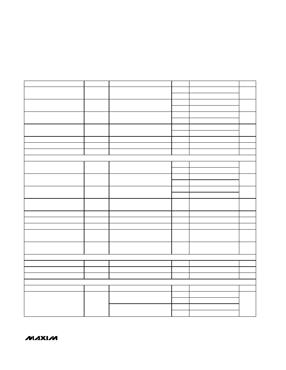
_______________________________________________________________________________________
PARAMETER
SYM B O L CONDITIONS
T
A
MIN
TYP
MAX
UNITS
ANALOG SWITCH
Fault-Free Analog Signal Range
V
COM_
,
V
NO_
, V
NC_
E
0
V+
V
+25
∞C
56
85
On-Resistance
R
ON
I
COM_
= 1mA,
V
NO_
, V
NC_
= +10V
E
120
+25
∞C
1.0
4
On-Resistance Match Between
Channels (Note 4)
R
ON
I
COM_
= 1mA,
V
NO_
, V
NC_
= +10V
E
5
+25
∞C
-0.25
+0.25
NO_, NC_ Off-Leakage Current
(Note 5)
I
NO_(OFF)
,
I
NC_(OFF)
V
COM_
= +1V, +10V,
V
NO_
, V
NC_
= +10V, +1V
E
-20
+20
nA
+25
∞C
-0.5
+0.25
COM_ Off-Leakage Current
(Note 5)
I
COM_(OFF)
V
COM_
= +1V, +10V,
V
NO_
, V
NC_
= +10V, +1V
E
-20
+20
nA
+25
∞C
-0.5
+0.5
COM_ On-Leakage Current
(Note 5)
I
COM_(ON)
V
COM_
= +1V, +10V,
V
NO_
, V
NC_
= +1V, +10V,
or floating
E
-40
+40
nA
FAULT
Power on
E
-36
+36
Fault-Protected Analog
Signal Range
V
COM_
,
V
NO_
,
V
NC_
Power off
E
-40
+40
V
+25
∞C
-1
+1
NO_ or NC_ Off-Leakage
Current (Note 5)
I
NO_
, I
NC_
V
NO_
, V
NC_
=
±36V
E
-10
+10
µA
+25
∞C
-1
+1
COM_ Off-Leakage Current
(Note 5)
I
COM_
V
NO_
, V
NC_
=
±36V
E
-10
+10
µA
+25
∞C
-1
+1
NO_ or NC_ Leakage Current
(Note 5)
I
NO_
,
I
NC_
Supplies off, V
NO_
, V
NC_
=
±40V
E
-10
+10
µA
PARAMETER
SYM B O L CONDITIONS
T
A
MIN
TYP
MAX
UNITS
+25∞C
155
250
All V
IN_
= +5V, V
COM_
= 0
E
325
+25∞C
155
250
V- Supply Current
I-
All V
IN_
= 0 or V+, V
COM_
= 0
E
325
µA
+25∞C
200
350
All V
IN_
= +5V, V
COM_
= 0
E
475
+25∞C
0.1
1
GND Supply Current
I
GND
All V
IN_
= 0 or V+, V
COM_
= 0
E
10
µA
ELECTRICAL CHARACTERISTICS--Single +12V Supply
(V+ = +12V, V- = 0, V
IH
= +2.4V, V
IL
= +0.8V, GND = 0, T
A
= T
MIN
to T
MAX
, unless otherwise noted. Typical values are at
T
A
= +25
∞C.) (Notes 2, 3)
ELECTRICAL CHARACTERISTICS--
±15V Dual Supplies (continued)
(V+ = +15V, V- = -15V, V
IH
= +2.4V, V
IL
= +0.8V, GND = 0, T
A
= T
MIN
to T
MAX
, unless otherwise noted. Typical values are at
T
A
= +25
∞C.) (Notes 2, 3)

DG411F/DG412F/DG413F
Quad, Rail-to-Rail, Fault-Protected,
SPST Analog Switches
_______________________________________________________________________________________
5
Note 2: The algebraic convention is used in this data sheet; the most negative value is shown in the minimum column.
Note 3: Electrical specifications at -40
∞C are not production tested and guaranteed by design.
Note 4:
R
ON
=
R
ON(MAX)
-
R
ON(MIN)
.
Note 5: Leakage parameters are 100% tested at maximum rated temperature and with dual supplies and guaranteed by design at +25∞C.
Note 6: Guaranteed by design.
Note 7: Off-Isolation = 20 log
10
[V
COM
/(V
NC
or V
NO
)], V
COM
= output, V
NC
or V
NO
= input to off switch.
Note 8: Between any two switches.
ELECTRICAL CHARACTERISTICS--Single +12V Supply (continued)
(V+ = +12V, V- = 0, V
IH
= +2.4V, V
IL
= +0.8V, GND = 0, T
A
= T
MIN
to T
MAX
, unless otherwise noted. Typical values are at
T
A
= +25
∞C.) (Notes 2, 3)
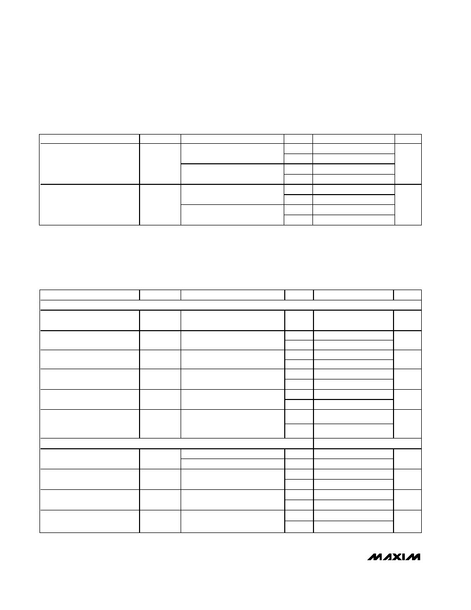
PARAMETER
SYM B O L
CONDITIONS
T
A
MIN
TYP
MAX
UNITS
+25
∞C
-1
+1
COM_ Leakage Current
(Note 5)
I
COM_
Supplies off, V
NO_
, V
NC_
=
±40V
E
-10
+10
µA
+Fault Output Turn-Off Delay
V
NO_
, V
NC_
= +36V, R
L
= 1k
E
20
ns
+Fault Recovery Time
V
NO_
, V
NC_
= +36V, R
L
= 1k
E
1
µs
SWITCH DYNAMICS
+25
∞C
120
250
Turn-On Time
t
ON
V
NO_
or V
NC_
= +10V, R
L
= 300
,
C
L
= 35pF, Figure 2
E
315
ns
+25
∞C
70
125
Turn-Off Time
t
OFF
V
NO_
or V
NC_
= +10V, R
L
= 300
,
C
L
= 35pF, Figure 2
E
140
ns
+25
∞C
2
50
Break-Before-Make Time Delay
(DG413F Only) (Note 6)
t
BBM
V
NO_
or V
NC_
= +10V, R
L
= 100
,
C
L
= 10pF, Figure 3
E
1
ns
Charge Injection
Q
V
GEN
= 0, R
GEN
= 0, C
L
= 1nF,
Figure 4
+25
∞C
5
pC
LOGIC INPUT
Input Logic High
V
IH
E
2.4
V
Input Logic Low
V
IL
E
0.8
V
Input Leakage Current
(Note 5)
I
IN
V
IN_
= 0 or V+
E
-1
+1
µA
POWER SUPPLY
Power-Supply Range
V+
E
+9
+36
V
+25
∞C
180
350
All V
IN_
= +5V, V
COM_
= +6V
E
450
+25
∞C
85
150
V+ Supply Current
I+
All V
IN_
= 0 or V+, V
COM_
= +6V
E
250
µA

DG411F/DG412F/DG413F
Quad, Rail-to-Rail, Fault-Protected,
SPST Analog Switches
6
_______________________________________________________________________________________
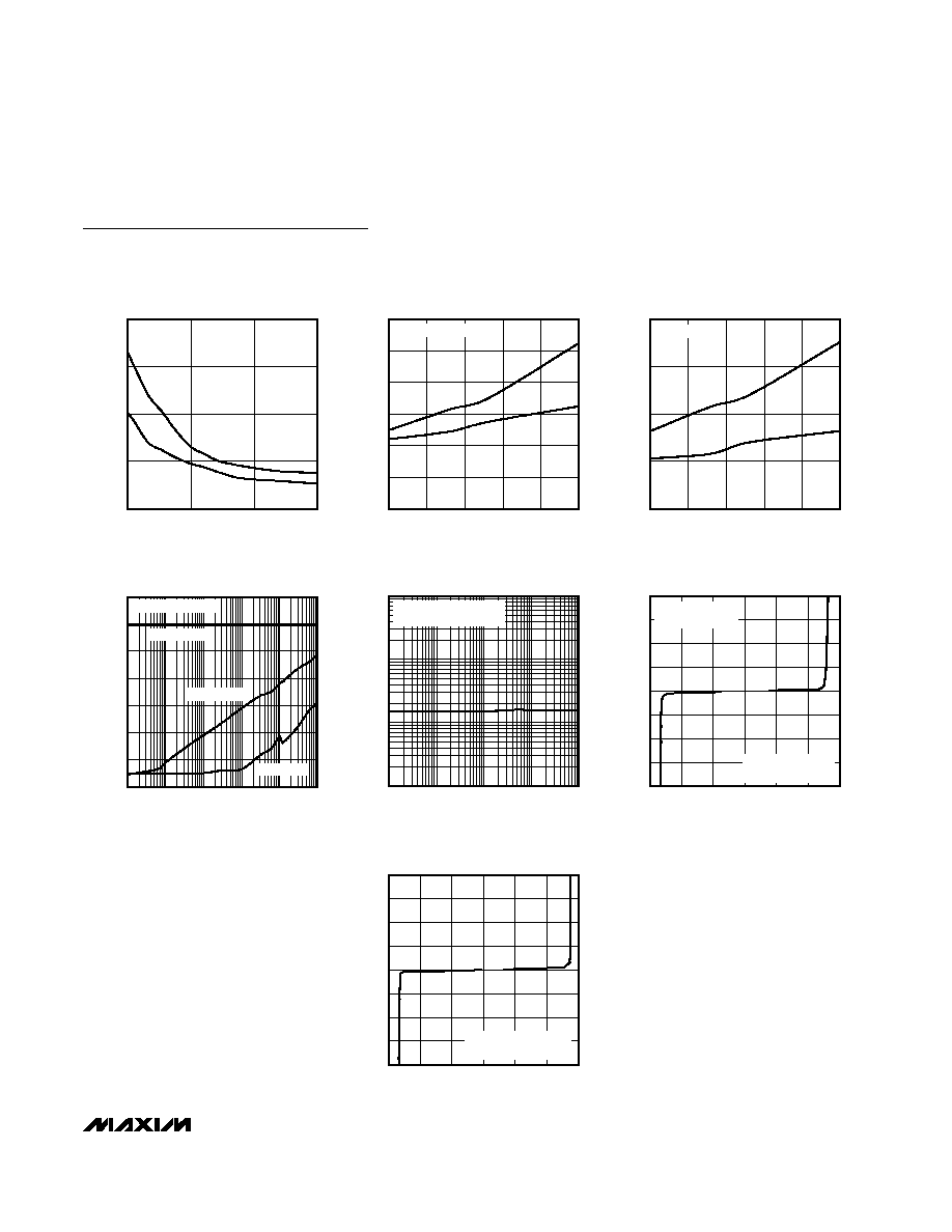
Typical Operating Characteristics
(T
A
= +25∞C, unless otherwise noted.)
TURN-ON/TURN-OFF TIMES
vs. SUPPLY VOLTAGE (DUAL SUPPLIES)
DG411 toc09
SUPPLY VOLTAGE (V+, V-)
t
ON
/t
OFF
(ns)
15
10
50
100
150
200
250
300
0
5
20
t
ON
t
OFF
LOGIC-LEVEL THRESHOLD VOLTAGE
vs. SUPPLY VOLTAGE
DG411 toc08
SUPPLY VOLTAGE (V)
THRESHOLD VOLTAGE (V)
35
30
25
20
15
10
1.5
2.0
2.5
3.0
1.0
5
40
DUAL OR SINGLE
SUPPLIES
SUPPLY CURRENT vs. TEMPERATURE
DG411 toc07
TEMPERATURE (
∞C)
SUPPLY CURRENT (
µ
A)
60
35
10
-15
100
200
300
400
500
0
-40
85
DUAL SUPPLIES:
V+ = +15V, V- = -15V, V
IN_
= +5V
I+
I-
I
GND
CHARGE INJECTION vs. V
COM
DG411 toc06
V
COM
(V)
Q (pC)
10
5
0
-5
-10
-10
0
10
20
30
40
-20
-15
15
DUAL SUPPLIES:
±15V
SINGLE
SUPPLY: +12V
ON/OFF-LEAKAGE CURRENT
vs. TEMPERATURE
DG411 toc05
TEMPERATURE (
∞C)
LEAKAGE CURRENT (pA)
60
35
10
-15
0.1
1
10
100
1000
10,000
0.01
-40
85
I
COM(ON)
I
COM(OFF)
I
NO(OFF)
,
I
NC(OFF)
DUAL SUPPLIES:
V+ = +15V, V- = -15V
ON-RESISTANCE vs. V
COM
AND TEMPERATURE
(SINGLE SUPPLY)
DG411 toc04
V
COM
(V)
R
ON
(
)
10
8
6
4
2
20
40
60
80
100
0
0
12
V+ = +12V
V- = 0
T
A
= +85
∞C
T
A
= +25
∞C
T
A
= -40
∞C
ON-RESISTANCE vs. V
COM
(SINGLE SUPPLY)
DG411 toc03
V
COM
(V)
R
ON
(
)
30
24
18
12
6
20
40
60
80
100
0
0
36
V+ = +9V
V- = 0
V+ = +12V
V- = 0
V+ = +15V
V- = 0
V+ = +24V
V- = 0
V+ = +36V
V- = 0
V+ = +28V
V- = 0
ON-RESISTANCE vs. V
COM
AND TEMPERATURE
(DUAL SUPPLIES)
DG411 toc02
V
COM
(V)
R
ON
(
)
10
5
0
-5
-10
10
20
30
40
50
0
-15
15
V+ = +15V
V- = -15V
T
A
= +85
∞C
T
A
= +25
∞C
T
A
= -40
∞C
ON-RESISTANCE vs. V
COM
(DUAL SUPPLIES)
DG411 toc01
V
COM
(V)
R
ON
(
)
15
10
5
0
-5
-10
-15
20
40
60
80
100
0
-20
20
V+ = +5V
V- = -5V
V+ = +10V
V- = -10V
V+ = +15V
V- = -15V
V+ = +20V
V- = -20V
DG411F/DG412F/DG413F
Quad, Rail-to-Rail, Fault-Protected,
SPST Analog Switches
_______________________________________________________________________________________
7
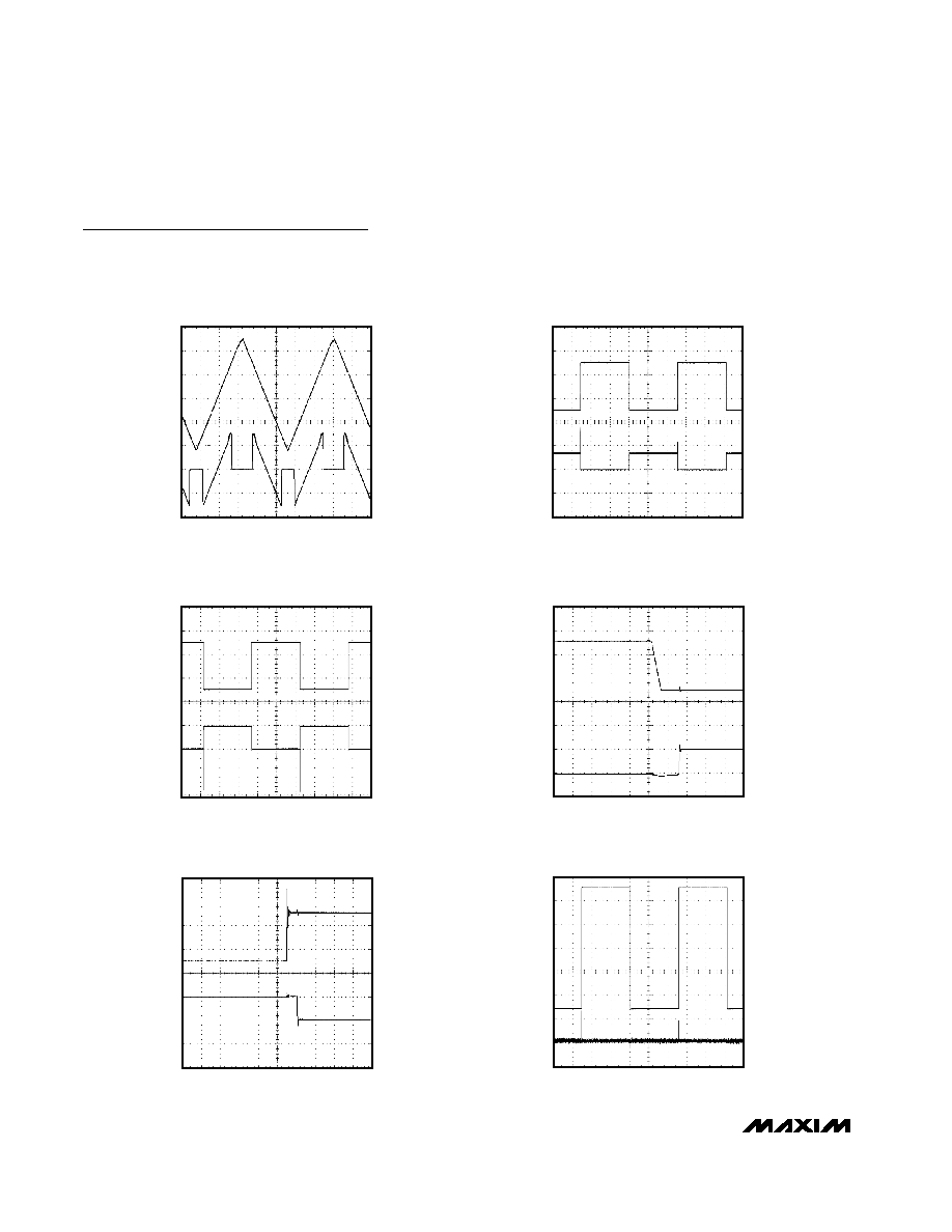
Typical Operating Characteristics (continued)
(T
A
= +25∞C, unless otherwise noted.)
FAULT CURRENT vs. FAULT VOLTAGE
(SINGLE SUPPLY)
DG411 toc16
V
COM
(V)
I
COM
(
µ
A)
40
20
-40
-20
0
-150
-100
-50
0
50
100
150
200
-200
-60
60
FOR 0V < V
COM
< V
SUPPLY
,
I
COM
= V
COM
/R
L
FAULT CURRENT vs. FAULT VOLTAGE
(DUAL SUPPLIES)
DG411 toc15
V
COM
(V)
I
COM
(
µ
A)
40
20
-40
-20
0
-150
-100
-50
0
50
100
150
200
-200
-60
60
DUAL SUPPLIES:
V+ = +15V, V- = -15V
FOR |V
COM
| < V
SUPPLY
,
I
COM
= V
COM
/R
L
TOTAL HARMONIC DISTORTION
vs. FREQUENCY
DG411 toc14
FREQUENCY (Hz)
THD (%)
10k
1k
100
0.01
0.1
1
0.001
10
100k
±15V DUAL SUPPLIES
IN = OUT = 600
, V
P-P
= 5V
FREQUENCY RESPONSE
DG411 toc13
FREQUENCY (MHz)
LOSS (dB)
10
1
0.1
0.01
-100
-80
-60
-40
-20
0
20
-120
0.001
100
V+ = +15V, V- = -15V
ON-RESPONSE
OFF-ISOLATION
CROSSTALK
TURN-ON/TURN-OFF TIMES
vs. TEMPERATURE (SINGLE SUPPLY)
DG411 toc12
TEMPERATURE (
∞C)
t
ON
/t
OFF
(ns)
60
35
10
-15
50
100
150
200
0
-40
85
t
ON
t
OFF
V+ = +12V, V- = 0
TURN-ON/TURN-OFF TIMES
vs. TEMPERATURE (DUAL SUPPLIES)
DG411 toc11
TEMPERATURE (
∞C)
t
ON
/t
OFF
(ns)
60
35
10
-15
20
40
60
80
100
120
0
-40
85
t
ON
t
OFF
DUAL SUPPLIES:
±15V
TURN-ON/TURN-OFF TIMES
vs. SUPPLY VOLTAGE (SINGLE SUPPLY)
DG411 toc10
SUPPLY VOLTAGE (V+)
t
ON
/t
OFF
(ns)
27
18
50
100
150
200
0
9
36
t
ON
t
OFF
V- = GND
DG411F/DG412F/DG413F
Quad, Rail-to-Rail, Fault-Protected,
SPST Analog Switches
8
_______________________________________________________________________________________
Typical Operating Characteristics (continued)
(T
A
= +25∞C, unless otherwise noted.)
FAULT RESPONSE
(V+ = 0, V- = -15V)
DG411 toc22
2ms/div
GND
V
COM_
OUTPUT
V
NO_
, V
NC_
INPUT
+25V
GND
-25V
FAULT RECOVERY TIME
(NEGATIVE INPUT)
DG411 toc21
1
µs/div
GND
V
COM_
OUTPUT
-5V
V
NO_
, V
NC_
INPUT
-5V
GND
-25V
FAULT RECOVERY TIME
(POSITIVE INPUT)
DG411 toc20
1
µs/div
GND
V
COM_
OUTPUT
+5V
V
NO_
, V
NC_
INPUT
+25V
GND
+5V
FAULT STEP RESPONSE
(NEGATIVE INPUT)
DG411 toc19
2ms/div
GND
V
COM_
OUTPUT
-5V
-5V
V
NO_
, V
NC_
INPUT
-25V
GND
FAULT STEP RESPONSE
(POSITIVE INPUT)
DG411 toc18
GND
V
COM_
OUTPUT
GND
V
NO_
, V
NC_
INPUT
2ms/div
+5V
+25V
INPUT OVERVOLTAGE vs. OUTPUT
DG411 toc17
GND
+25V
+15V
-22V
-15V
V
COM_
OUTPUT
GND
V
NO_
, V
NC_
INPUT
20ms/div
Detailed Description
The DG411F/DG412F/DG413F are fault-protected
CMOS analog switches with unique operation and
construction. These switches differ considerably from
traditional fault-protection switches, with several advan-
tages. First, they are constructed with two parallel
FETs, allowing very low on-resistance when the switch
is on. Second, they allow signals on the NO_ or NC_
pins that are within, or slightly beyond, the supply rails
to be passed through the switch to the COM_ terminal
(or vice versa), allowing true rail-to-rail signal operation.
Third, the DG411F/DG412F/DG413F have the same
fault-protection performance on any of the NO_, NC_,
or COM_ switch inputs. Operation is identical for both
fault polarities. The fault protection extends to ±36V
from GND with
±15V supplies.
During a fault condition, the particular overvoltage input
(COM_, NO_, NC_) pin becomes high impedance
regardless of the switch state or load resistance. When
power is removed, the fault protection is still in effect. In
this case, the COM_, NO_, or NC_ terminals are a virtu-
al open circuit. The fault can be up to ±40V with power
off. The switches turn off when V+ is not powered,
regardless of V-.
Pin Compatibility
These switches have identical pinouts to common non-
fault-protected CMOS switches. They allow for carefree
direct replacement in existing printed circuit boards
since the NO_, NC_, and COM_ pins of each switch are
fault protected.
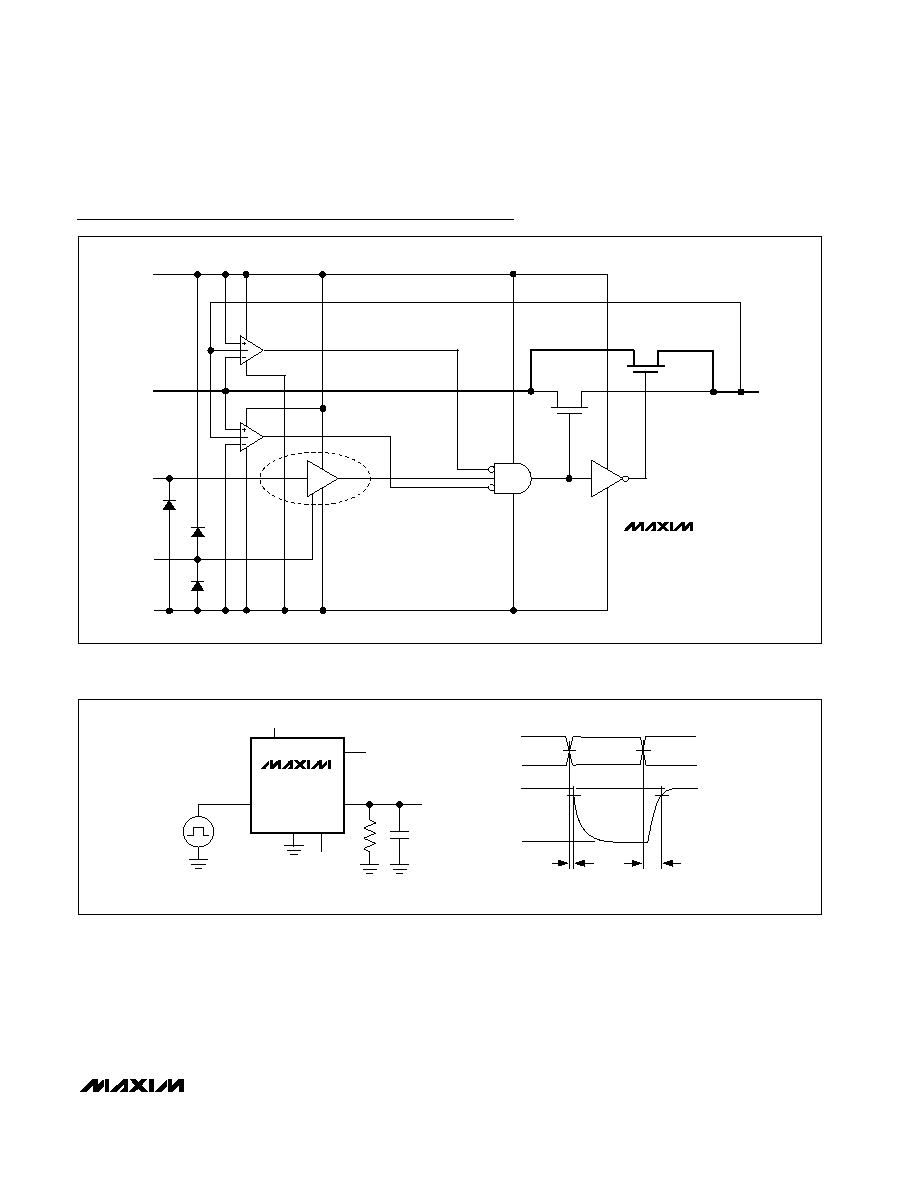
Internal Construction
Internal construction is shown in Figure 1, with the ana-
log signal paths shown in bold. A single NO switch is
shown. The NC configuration is identical except the
logic-level translator becomes an inverter. The analog
switch is formed by the parallel combination of N-chan-
nel FET (N1) and P-channel FET (P1), which are driven
on and off simultaneously according to the input fault
condition and the logic-level state.
Normal Operation
Two comparators continuously compare the voltage on
the COM_, NO_, and NC_ pins with V+ and V-. When
the signal on COM_, NO_, or NC_ is between V+ and
V-, the switch acts normally, with FETs N1 and P1 turn-
ing on and off in response to IN_ signals. The parallel
combination of N1 and P1 forms a low-value resistor
between NO_ (or NC_) and COM_ so that signals pass
equally well in either direction.
Positive Fault Condition
When the signal on NO_ (or NC_) and COM_ exceeds
V+ by about 50mV, the high-fault comparator output is
high, turning off FETs N1 and P1. This makes the NO_
(or NC_) and COM_ pins high impedance regardless of
DG411F/DG412F/DG413F
Quad, Rail-to-Rail, Fault-Protected,
SPST Analog Switches
_______________________________________________________________________________________
9
PIN
DG411F
DG412F
DG413F
NAME
FUNCTION
1, 16, 9, 8
1, 16, 9, 8
1, 16, 9, 8
IN1, IN2, IN3, IN4
Logic Control Digital Inputs
2, 15, 10, 7
2, 15, 10, 7
2, 15, 10, 7
COM1, COM2, COM3,
COM4
Analog Switch Common Terminals
3, 14, 11, 6
--
--
NC1, NC2, NC3, NC4
Analog Switch Normally Closed Terminals
--
3, 14, 11, 6
--
NO1, NO2, NO3, NO4
Analog Switch Normally Open Terminals
--
--
3, 6
NO1, NO4
Analog Switch Normally Open Terminals
--
--
14, 11
NC2, NC3
Analog Switch Normally Closed Terminals
4
4
4
V-
Negative-Supply Voltage Input. Connect to GND for single-
supply operation. Bypass with a 0.1µF capacitor to GND.
5
5
5
GND
Ground. Connect to digital ground.
12
12
12
N.C.
No Connection. Not internally connected.
13
13
13
V+
Positive-Supply Voltage Input. Bypass with a 0.1µF capacitor
to GND.
Pin Description
DG411F/DG412F/DG413F
the switch state. If the switch state is off, all FETs are
turned off and both NO_ (or NC_) and COM_ are high
impedance.
Negative Fault Condition
When the signal on NO_ (or NC_) and COM_ exceeds
V- by about 50mV, the low-fault comparator output is
high, turning off FETs N1 and P1. This makes the NO_
(or NC_) and COM_ pins high impedance regardless of
the switch state. If the switch state is off, all FETs are
turned off and both NO_ (or NC_) and COM_ are high
impedance.
Transient Fault Response and Recovery
When a fast rise-time and fall-time transient on NO_,
NC_, or COM_ exceeds V+ or V-, the output follows the
input to the supply rail with only a few nanoseconds
delay. This delay is due to the switch on-resistance and
circuit capacitance to ground. When the input transient
returns to within the supply rails, however, there is a
longer output recovery time delay. For positive faults,
the recovery time is typically 1µs. For negative faults,
the recovery time is typically 0.5µs. These values
depend on the output resistance and capacitance, and
are not production tested or guaranteed. The delays
are not dependent on the fault amplitude. Higher load
resistance and capacitance increase recovery times.
Fault-Protection Voltage and Power Off
The maximum fault voltage on the NO_ (or NC_) and
COM_ pins is ±36V with power applied and ±40V with
power off.
Failure Modes
Exceeding the fault-protection voltage limits on NO_,
NC_, or COM_, even for very short periods, can cause
the device to fail. See the Absolute Maximum Ratings.
The failure modes may not be obvious, and failure in
one switch may or may not affect other switches in the
same package.
Ground
There is no galvanic connection between the analog
signal paths and GND. The analog signal paths consist
of an N-channel and P-channel MOSFET with their
sources and drains paralleled and their gates driven
out of phase to V+ and V- by the logic-level translators.
However, the potential of the analog signals must be
defined or at least limited with respect to GND.
V+ and GND power the internal logic and logic-level
translators and set the input logic thresholds. The logic-
level translators convert the logic levels to switched V+
and V- signals to drive the gates of the analog switch-
es. This drive signal is the only connection between the
power supplies and the analog signals.
IN_ Logic-Level Thresholds
The logic-level thresholds are CMOS and TTL compati-
ble when V+ is +15V. As V+ is raised, the threshold
increases slightly, and when V+ reaches 25V, the level
threshold is about 2.3V, above the TTL output high-level
minimum of 2.4V, but still compatible with CMOS out-
puts (see the Typical Operating Characteristics). V- has
no effect on the logic-level thresholds.
Bipolar Supplies
The DG411F/DG412F/DG413F operate with bipolar
supplies between ±4.5V and ±20V. The V+ and V- sup-
plies need not be symmetrical, but their difference can-
not exceed the absolute maximum rating of 44V.
Single Supply
The DG411F/DG412F/DG413F operate from a single
supply between +9V and +36V when V- is connected to
GND.
Chip Information
TRANSISTOR COUNT: 251
PROCESS: CMOS
SUBSTRATE CONNECTED TO: V+
Quad, Rail-to-Rail, Fault-Protected,
SPST Analog Switches
10
______________________________________________________________________________________
Ordering Information (continued)
PART
TEMP RANGE
PIN-PACKAGE
DG412FEUE
-40∞C to +85∞C
16 TSSOP
DG412FDY
-40∞C to +85∞C
16 SO
DG412FDJ
-40∞C to +85∞C
16 Plastic DIP
DG413FEUE
-40∞C to +85∞C
16 TSSOP
DG413FDY
-40∞C to +85∞C
16 SO
DG413FDJ
-40∞C to +85∞C
16 Plastic DIP
DG411F/DG412F/DG413F
Quad, Rail-to-Rail, Fault-Protected,
SPST Analog Switches
______________________________________________________________________________________
11
Test Circuits/Timing Diagrams
Figure 1. Functional Diagram
NORMALLY OPEN SWITCH CONSTRUCTION
COM_
DG411F
DG412F
DG413F
P1
N1
ON
LOW
FAULT
HIGH
FAULT
V+
NO_
IN_
GND
ESD DIODE
V-
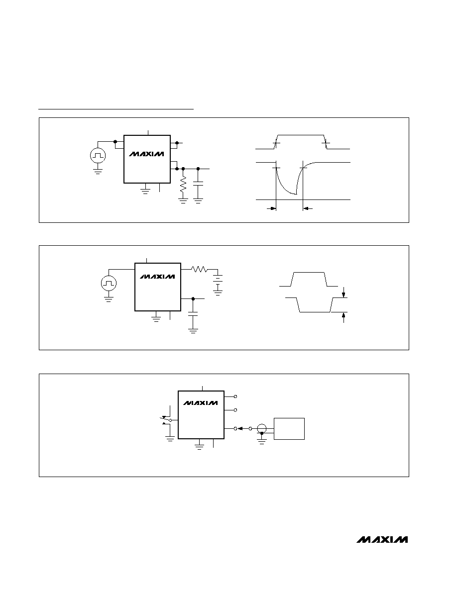
Figure 2. Switch Turn-On/Turn-Off Times
50%
t
ON
3V
0V
V
IN_
0V
90%
t
OFF
V
IN_
V+
GND
V+
NO_ OR NC_
COM_
10V
R
L
C
L
V-
V-
V- IS CONNECTED TO GND (0V) FOR SINGLE-SUPPLY OPERATION.
10V
V
OUT
V
OUT
DG411F
DG412F
DG413F
90%
DG411F/DG412F/DG413F
Quad, Rail-to-Rail, Fault-Protected,
SPST Analog Switches
12
______________________________________________________________________________________
Test Circuits/Timing Diagrams (continued)
Figure 3. DG413F Break-Before-Make Interval
V
IN_
V+
GND
V+
NO_
COM_
10V
R
L
C
L
V-
V-
V- IS CONNECTED TO GND (0V) FOR SINGLE-SUPPLY OPERATION.
V
OUT
DG413F
COM_
NC_
IN_
IN_
50%
3V
0V
V
NO_
, V
NC_
V
OUT
V
IN_
0V
90%
t
BBM
t
R
< 5ns
t
F
< 5ns
Figure 4. Charge Injection
V
IN_
V+
GND
V+
NO_ OR NC_
COM_
C
L
V-
V-
V- IS CONNECTED TO GND (0V) FOR SINGLE-SUPPLY OPERATION.
V
OUT
DG411F
DG412F
DG413F
IN_
R
GEN
V
GEN
0V
3V
V
OUT
V
IN_
V
OUT
V
OUT
IS THE MEASURED VOLTAGE DUE TO CHARGE-
TRANSFER ERROR Q WHEN THE CHANNEL TURNS OFF
Q =
V
OUT
x C
L
Figure 5. COM_, NO_, NC_ Capacitance
V+
GND
V+
NO_
COM_
V-
V-
V- IS CONNECTED TO GND (0V) FOR SINGLE-SUPPLY OPERATION.
DG411F
DG412F
DG413F
IN_
NC_
V+
1MHz
CAPACITANCE
ANALYZER
DG411F/DG412F/DG413F
Quad, Rail-to-Rail, Fault-Protected,
SPST Analog Switches
______________________________________________________________________________________
13
Test Circuits/Timing Diagrams (continued)
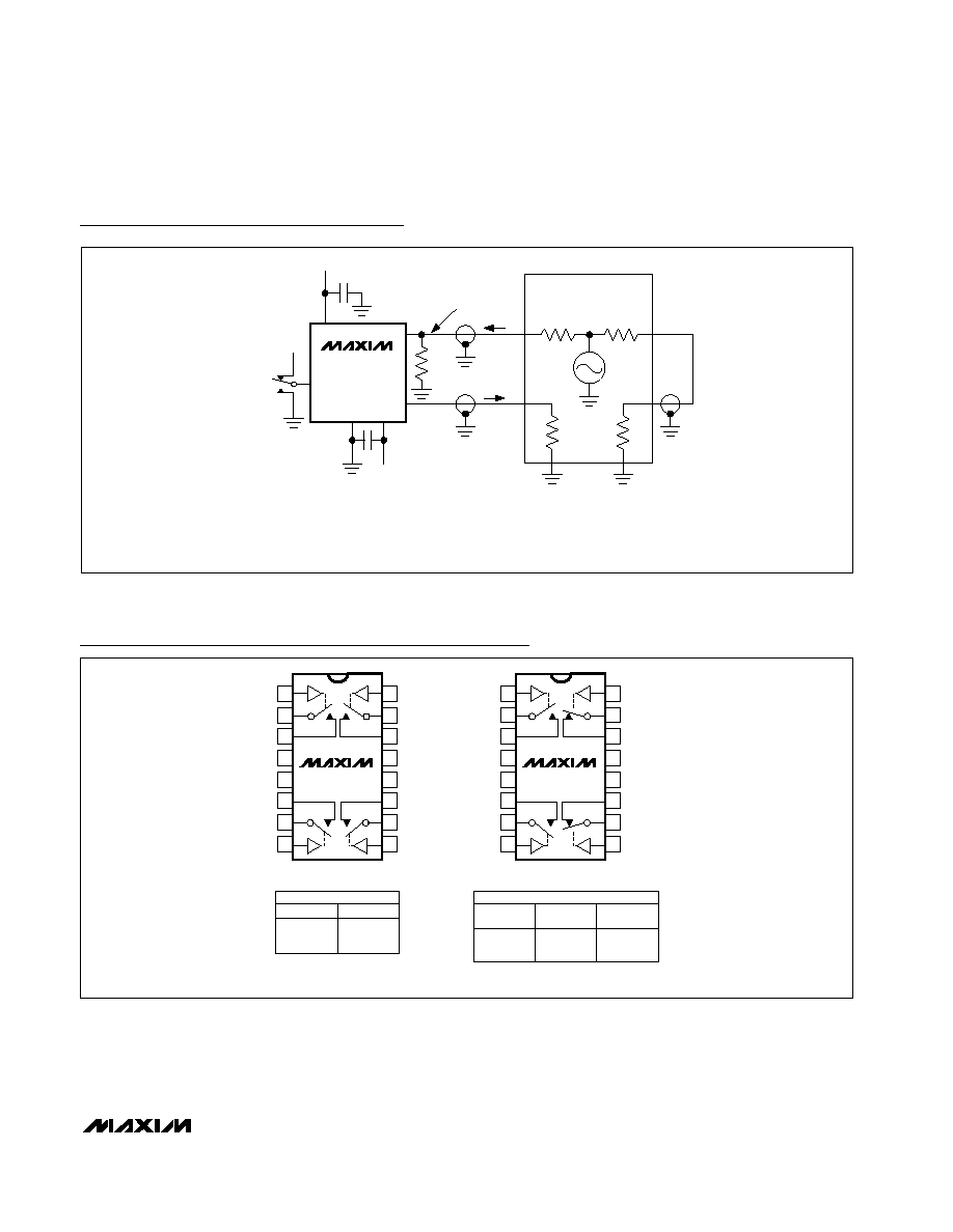
Figure 6. Frequency Response, Off-Isolation, and Crosstalk
V+
GND
V+
COM_
NO_, NC_
V-
V-
MEASUREMENTS ARE STANDARDIZED AGAINST SHORT AND OPEN AT SOCKET TERMINALS.
OFF-ISOLATION IS MEASURED BETWEEN COM_ AND "OFF" NO_ OR NC_ TERMINALS.
ON-RESPONSE IS MEASURED BETWEEN COM_ AND "ON" NO_ OR NC_ TERMINALS.
CROSSTALK IS MEASURED BETWEEN COM_ TERMINALS WITH ALL SWITCHES ON.
V- IS CONNECTED TO GND (0V) FOR SINGLE-SUPPLY OPERATION.
DG411F
DG412F
DG413F
IN_
10nF
10nF
V
IN
V
OUT
NETWORK
ANALYZER
50
50
50
50
MEAS
REF
50
50
RESISTOR
ONLY NEEDED
FOR CROSSTALK
AND ISOLATION
3.0V
N.C. = NOT CONNECTED. SWITCHES SHOWN FOR LOGIC "0" INPUT.
ALL SWITCHES ARE OFF WITH POWER REMOVED
DIP/TSSOP/SO
DG412F
LOGIC
SWITCH
0
1
OFF
ON
TOP VIEW
DIP/TSSOP/SO
DG413F
LOGIC
SWITCHES
1, 4
0
1
OFF
ON
SWITCHES
2, 3
ON
OFF
16
15
14
13
12
11
10
9
1
2
3
4
5
6
7
8
IN2
COM2
NC2
V+
V-
NO1
COM1
IN1
DG413F
N.C.
NC3
COM3
IN3
IN4
COM4
NO4
GND
16
15
14
13
12
11
10
9
1
2
3
4
5
6
7
8
IN2
COM2
NO2
V+
V-
NO1
COM1
IN1
DG412F
N.C.
NO3
COM3
IN3
IN4
COM4
NO4
GND
Pin Configurations (continued)
DG411F/DG412F/DG413F
Quad, Rail-to-Rail, Fault-Protected,
SPST Analog Switches
14
______________________________________________________________________________________
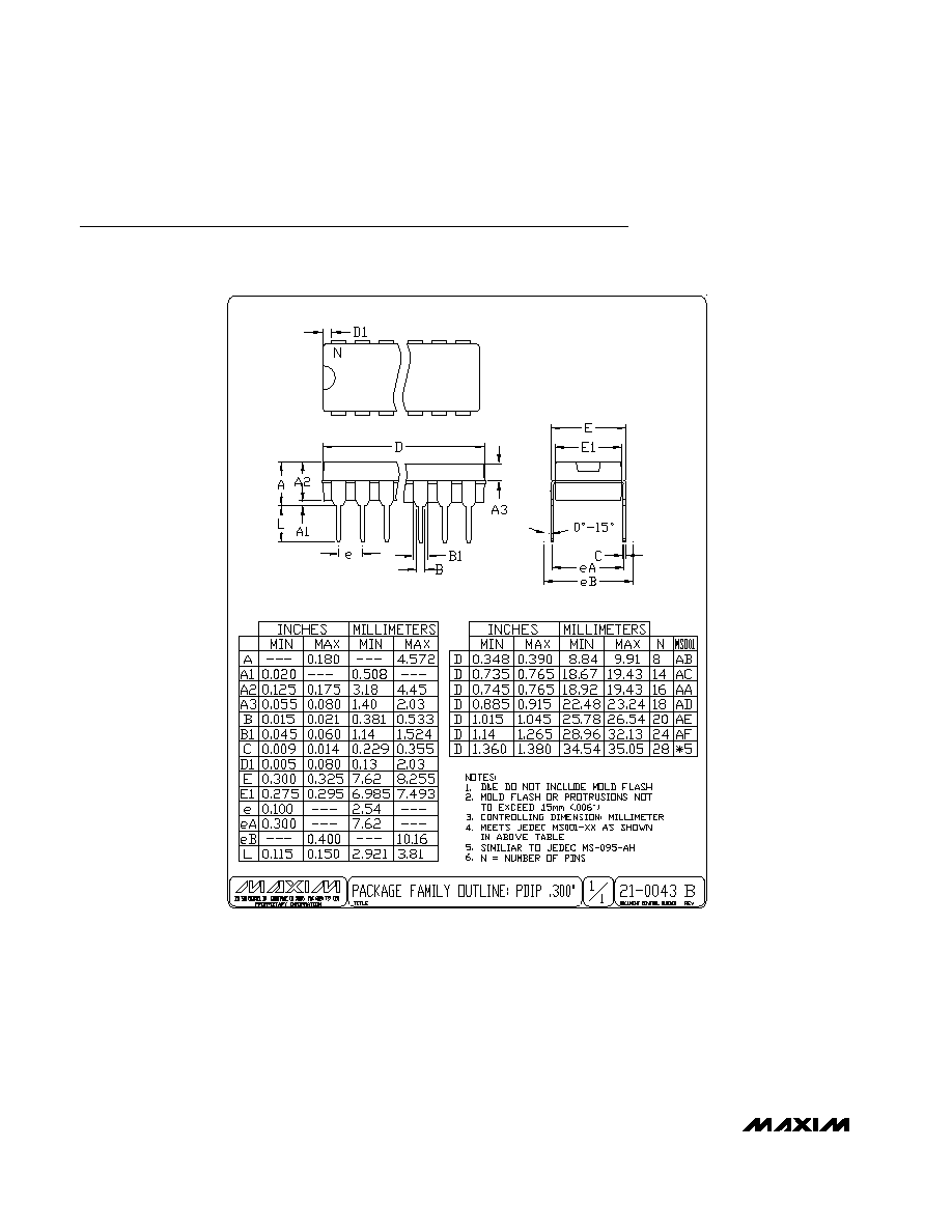
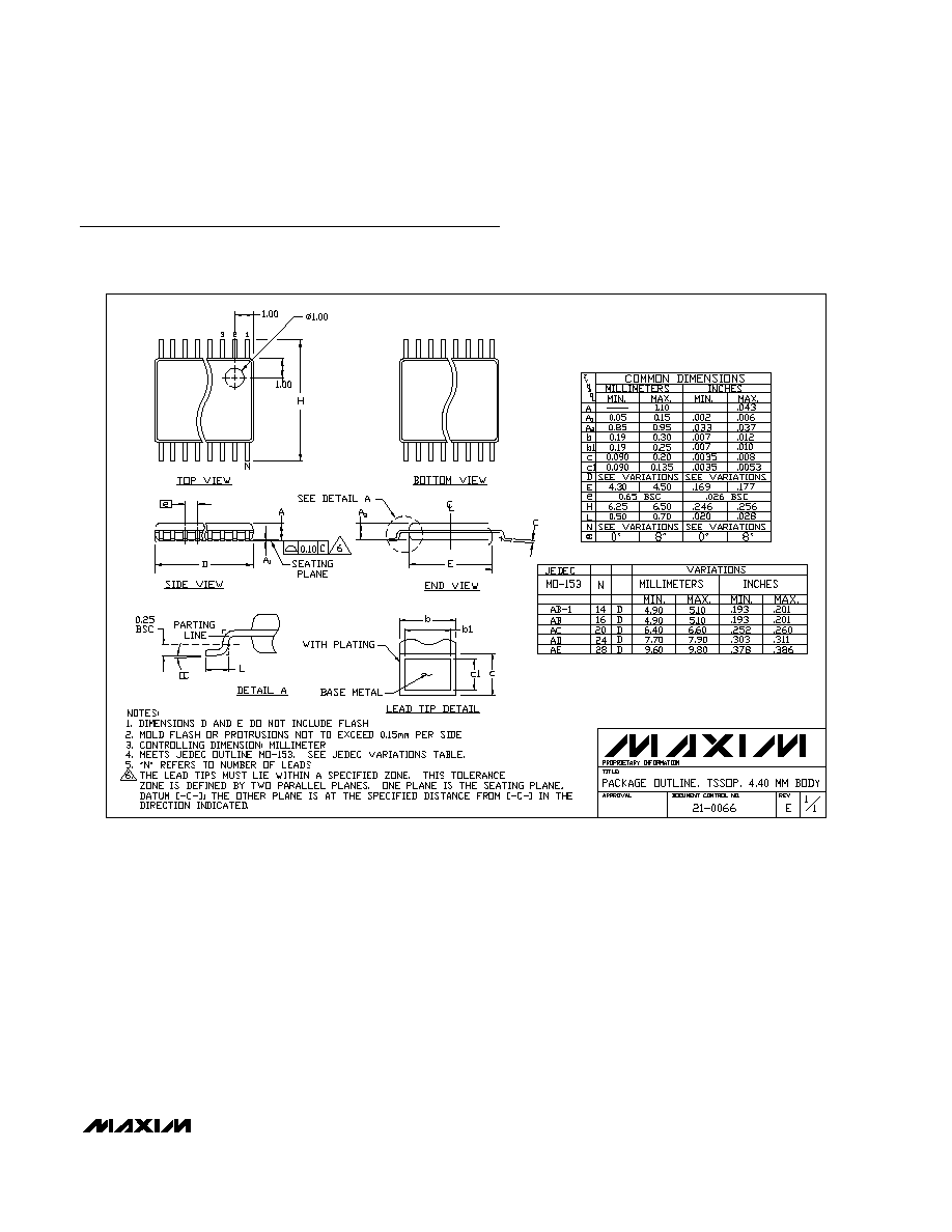
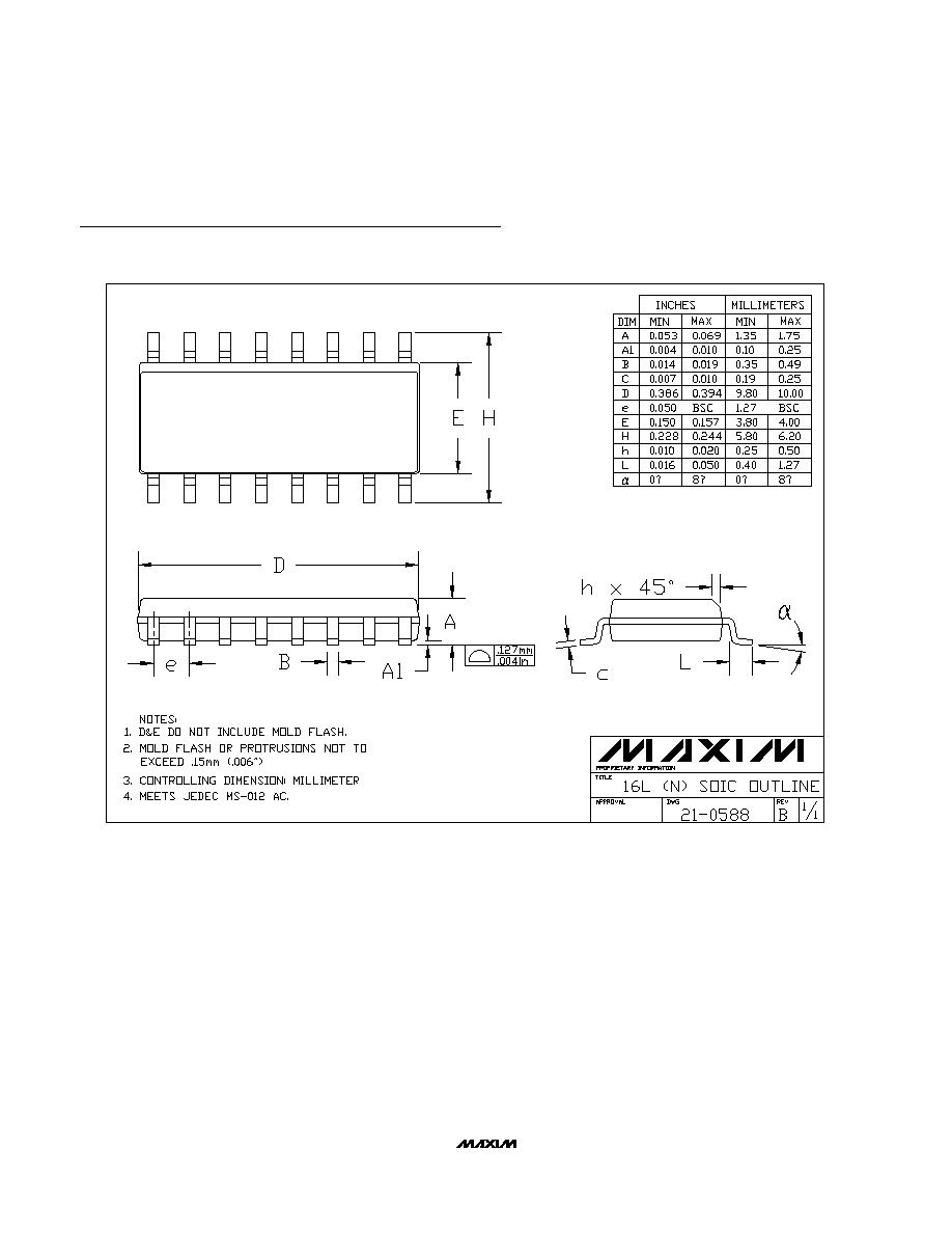
Package Information
(The package drawing(s) in this data sheet may not reflect the most current specifications. For the latest package outline information,
go to www.maxim-ic.com/packages.)
PDIPN.EPS
DG411F/DG412F/DG413F
Quad, Rail-to-Rail, Fault-Protected,
SPST Analog Switches
______________________________________________________________________________________
15
Package Information (continued)
(The package drawing(s) in this data sheet may not reflect the most current specifications. For the latest package outline information,
go to www.maxim-ic.com/packages.)
TSSOP,NO PADS.EPS
DG411F/DG412F/DG413F
Quad, Rail-to-Rail, Fault-Protected,
SPST Analog Switches
Maxim cannot assume responsibility for use of any circuitry other than circuitry entirely embodied in a Maxim product. No circuit patent licenses are
implied. Maxim reserves the right to change the circuitry and specifications without notice at any time.
16 ____________________Maxim Integrated Products, 120 San Gabriel Drive, Sunnyvale, CA 94086 408-737-7600
© 2002 Maxim Integrated Products
Printed USA
is a registered trademark of Maxim Integrated Products.
Package Information (continued)
(The package drawing(s) in this data sheet may not reflect the most current specifications. For the latest package outline information,
go to www.maxim-ic.com/packages.)
16L SOIC.EPS