SCOPE: SPST/SPDT ANALOG SWITCHES
Device Type Generic Number Circuit Function
01
DG417A(x)/883B CMOS, SPST analog switch
02
DG418A(x)/883B CMOS, SPST analog switch
03 DG419A(x)/883B CMOS, SPDT analog switch
Case Outline(s). The case outlines shall be designated in Mil-Std-1835 and as follows:
Outline Letter Mil-Std-1835 Case Outline Package Code
Maxim SMD
K P
GDIP1-T08 or CDIP2-T08 8 LEAD CERDIP J08
L X CDFP3-F10 10 LEAD FLATPACK F10
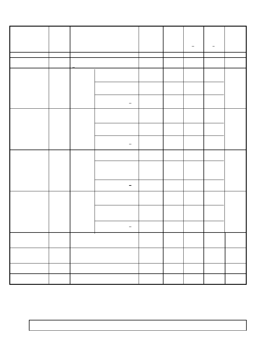
Absolute Maximum Ratings
Voltage Referenced to V
-
V
+
...................................................................................................................................... 44V
GND ................................................................................................................................. 25V
V
L
................................................................................................. (GND-0.3V) to (V
+
+0.3V)
Digital Inputs, V
S
, V
D
1/ ........................................................................(V
-
-2V) to (V
+
+2V)
or 30mA whichever occurs first.
Continuous Current, Any terminal ................................................................................ 30mA
Peak Current, S or D (Pulsed at 1ms, 10% duty cycle max) ....................................... 100mA
Lead Temperature (soldering, 10 seconds) ...................................................................... +300
∞
C
Storage Temperature ......................................................................................... -65
∞
C to +150
∞
C
Continuous Power Dissipation .... ............................................................................. T
A
=
+
70
∞
C
8 lead CERDIP(derate 8.0mW/
∞
C above +70
∞
C) ........................................................ 640mW
10 lead FLATPACK(derate 5.3mW/
∞
C above +70
∞
C) .................................................. 421mW
Junction Temperature T
J
............................................................................................. +150
∞
C
Thermal Resistance, Junction to Case,
JC:
Case Outline 8 lead CERDIP........................................................................ 55
∞
C/W
Case Outline 10 lead FLATPACK ................................................................. 85
∞
C/W
Thermal Resistance, Junction to Ambient,
JA:
Case Outline 8 lead CERDIP...................................................................... 125
∞
C/W
Case Outline 10 lead FLATPACK ............................................................... 190
∞
C/W
Recommended Operating Conditions
Ambient Operating Range (T
A
) .................................................................. -55
∞
C to
+
125
∞
C
Positive Supply Voltage (V
+
) ......................................................................................... +15V
Negative Supply Voltage (V
-
) ......................................................................................... -15V
V
INL
(max) ....................................................................................................................... 0.8V
V
INH
(min) ....................................................................................................................... 2.4V
Logic Supply Voltage (V
L
) ............................................................................................. +5V
1/ Signals on S, D or IN exceeding V
+
or V
-
are clamped by internal diodes. Limit forward current to
maximum current ratings.
Stresses beyond those listed under "Absolute Maximum Ratings" may cause permanent damage to the device.
These are stress ratings only, and functional operation of the device at these or any other conditions beyond
those indicated in the operational sections of the specifications is not implied. Exposure to absolute maximum
rating conditions for extended periods may affect device reliability.
----------------------------
Electrical Characteristics of DG417/418/419A /883B
19-0501
Rev. A
for SMD 5962-90737
Page 2 of
7

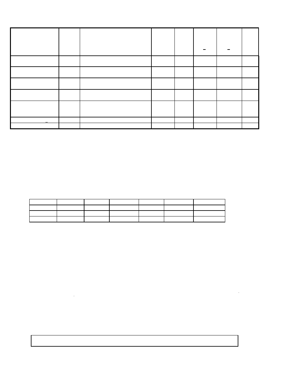
QUALITY ASSURANCE
Sampling and inspection procedures shall be in accordance with MIL-Prf-38535, Appendix A as specified in Mil-
Std-883.
Screening shall be in accordance with Method 5004 of Mil-Std-883. Burn-in test Method 1015:
1. Test Condition, A, B, C, or D.
2. TA = +125
∞
C minimum.
3. Interim and final electrical test requirements shall be specified in Table 2.
Quality conformance inspection shall be in accordance with Method 5005 of Mil-Std-883, including Groups A, B,
C, and D inspection.
Group A inspection:
1. Tests as specified in Table 2.
2. Selected subgroups in Table 1, Method 5005 of Mil-Std-883 shall be omitted.
Group C and D inspections:
a. End-point electrical parameters shall be specified in Table 1.
b. Steady-state life test, Method 1005 of Mil-Std-883:
1. Test condition A, B, C, D.
2. TA = +125
∞
C, minimum.
3. Test duration, 1000 hours, except as permitted by Method 1005 of Mil-Std-883.
TABLE 2. ELECTRICAL TEST REQUIREMENTS
Mil-Std-883 Test Requirements
Subgroups
per Method 5005, Table 1
Interim Electric Parameters
Method 5004
1
Final Electrical Parameters
Method 5005
1*, 2, 3, 9, 10, 11
Group A Test Requirements
Method 5005
1, 2, 3, 7**, 8**, 9, 10, 11
Group C and D End-Point Electrical Parameters
Method 5005
1
* PDA applies to Subgroup 1 only.
** Subgroups 7 and 8 tests shall be sufficient to verify the truth table.
----------------------------
Electrical Characteristics of DG417/418/419A /883B
19-0501
Rev. A
for SMD 5962-90737
Page 6 of
7