 | –≠–ª–µ–∫—Ç—Ä–æ–Ω–Ω—ã–π –∫–æ–º–ø–æ–Ω–µ–Ω—Ç: DG419CJ | –°–∫–∞—á–∞—Ç—å:  PDF PDF  ZIP ZIP |
_______________General Description
Maxim's redesigned DG417/DG418/DG419 precision,
CMOS, monolithic analog switches now feature guar-
anteed on-resistance matching (3
max) between
switches and guaranteed on-resistance flatness over
the signal range (4
max). These switches conduct
equally well in either direction and guarantee low
charge injection, low power consumption, and an ESD
tolerance of 2000V minimum per Method 3015.7. The
new design offers low off-leakage current over temper-
ature (less than 5nA at +85∞C).
The DG417/DG418 are single-pole/single-throw (SPST)
switches. The DG417 is normally closed, and the
DG418 is normally open. The DG419 is single-
pole/double-throw (SPDT) with one normally closed
switch and one normally open switch. Switching times
are less than 175ns max for t
ON
and less than 145ns
max for t
OFF
. Operation is from a single +10V to +30V
supply, or bipolar ±4.5V to ±20V supplies. The
improved DG417/DG418/DG419 are fabricated with a
44V silicon-gate process.
________________________Applications
Sample-and-Hold Circuits
Communications Systems
Test Equipment
Battery-Operated Systems
Modems
Fax Machines
Guidance and Control Systems
PBX, PABX
Audio Signal Routing
Military Radios
______________________New Features
o
Plug-In Upgrades for Industry-Standard
DG417/DG418/DG419
o
Improved R
DS(ON)
Match Between Channels
(3
max, DG419 only)
o
Guaranteed R
FLAT(ON)
Over Signal Range (4
max)
o
Improved Charge Injection (10pC max)
o
Improved Off-Leakage Current Over Temperature
(<5nA at +85∞C)
o
Withstand Electrostatic Discharge (2000V min)
per Method 3015.7
__________________Existing Features
o
Low R
DS(ON)
(35
max)
o
Single-Supply Operation +10V to +30V
Bipolar-Supply Operation
±
4.5V to
±
20V
o
Low Power Consumption (35µW max)
o
Rail-to-Rail Signal Handling
o
TTL/CMOS-Logic Compatible
DG417/DG418/DG419
Improved, SPST/SPDT Analog Switches
________________________________________________________________
Maxim Integrated Products
1
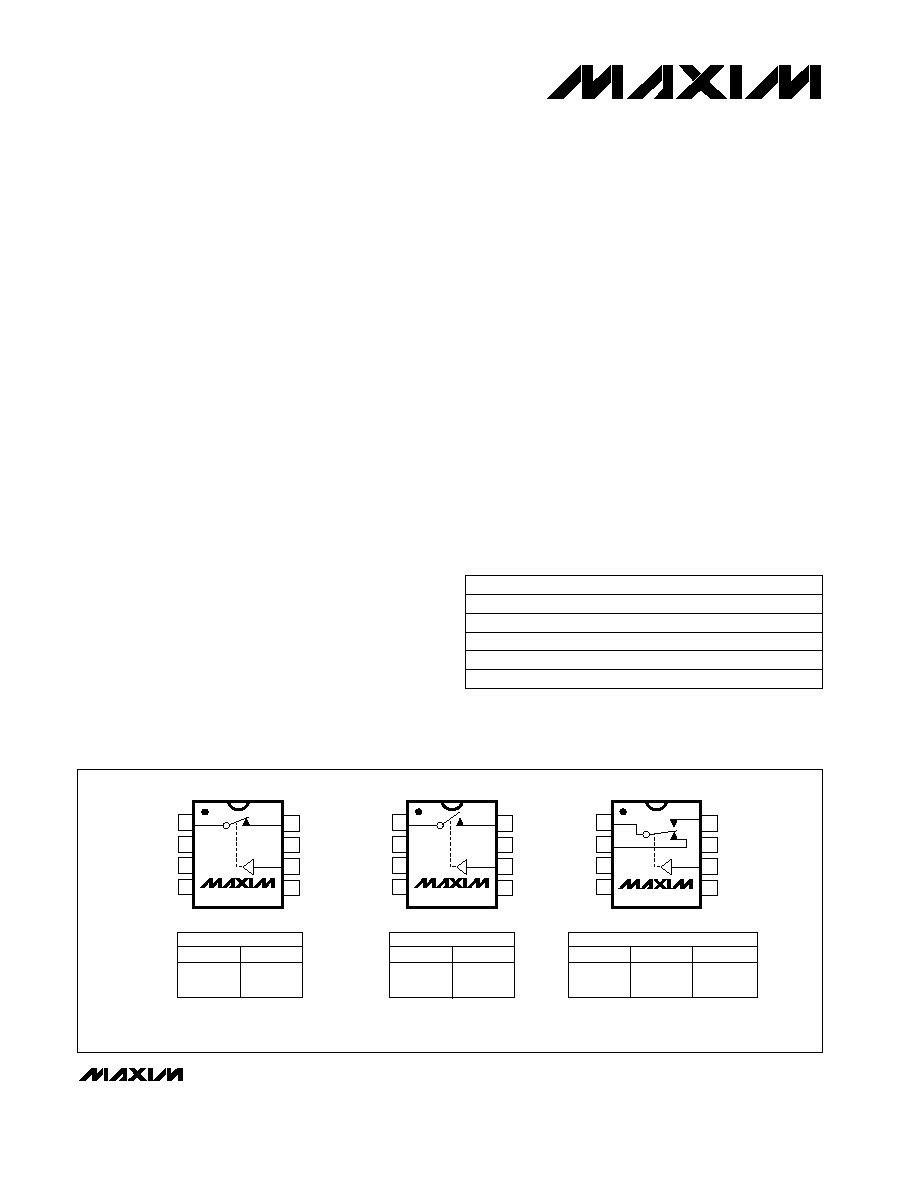
TOP VIEW
1
2
3
4
8
7
6
5
DG418
DIP/SO
1
2
3
4
8
7
6
5
D
V-
IN
VL
D
V-
IN
VL
V+
GND
N.C.
S
V+
GND
N.C.
S
DG417
DIP/SO
1
2
3
4
8
7
6
5
S2
V-
IN
VL
V+
GND
S1
D
DG419
DIP/SO
LOGIC
SWITCH
0
1
ON
OFF
SWITCHES SHOWN FOR LOGIC "0" INPUT
LOGIC
SWITCH
0
1
OFF
ON
LOGIC
SWITCH 1
0
1
ON
OFF
SWITCH 2
OFF
ON
DG417
DG418
DG419
N.C. = NO INTERNAL CONNECTION
_____________________Pin Configurations/Functional Diagrams/Truth Tables
19-0114; Rev 2; 12/96
PART
DG417
CJ
DG417CY
DG417C/D
0∞C to +70∞C
0∞C to +70∞C
0∞C to +70∞C
TEMP. RANGE
PIN-PACKAGE
8 Plastic DIP
8 SO
Dice*
______________Ordering Information
Ordering Information continued at end of data sheet.
* Contact factory for dice specifications.
For free samples & the latest literature: http://www.maxim-ic.com, or phone 1-800-998-8800
DG417DJ
DG417DY
-40∞C to +85∞C
-40∞C to +85∞C
8 Plastic DIP
8 SO
DG417/DG418/DG419
Improved, SPST/SPDT Analog Switches
2
_______________________________________________________________________________________
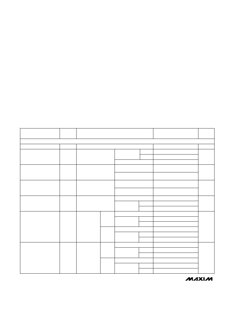
ABSOLUTE MAXIMUM RATINGS
ELECTRICAL CHARACTERISTICS--Dual Supplies
(V+ = +15V, V- = -15V, V
L
= 5V, GND = 0V, V
INL
= 0.8V, V
INH
= 2.4V, T
A
= T
MIN
to T
MAX
, unless otherwise noted.)
Stresses beyond those listed under "Absolute Maximum Ratings" may cause permanent damage to the device. These are stress ratings only, and functional
operation of the device at these or any other conditions beyond those indicated in the operational sections of the specifications is not implied. Exposure to
absolute maximum rating conditions for extended periods may affect device reliability.
Voltage Referenced to V-
V+ .......................................................................................44V
GND....................................................................................25V
VL ..................................................(GND - 0.3V) to (V+ + 0.3V)
Digital Inputs V
S
, V
D
(Note 1) .........(V- - 2V) to (V+ + 2V) or 30mA
(whichever occurs first)
Continuous Current (any terminal) (Note 1) ........................30mA
Peak Current, S or D (pulsed at 1ms, 10% duty cycle max)..100mA
Continuous Power Dissipation (T
A
= +70∞C)
Plastic DIP (derate 9.09mW/∞C above +70∞C) .............727mW
SO (derate 5.88mW/∞C above +70∞C) ..........................471mW
CERDIP (derate 8.00mW/∞C above +70∞C) ..................640mW
Operating Temperature Ranges
DG41_C_ .............................................................0∞C to +70∞C
DG41_D_ ..........................................................-40∞C to +85∞C
DG41_AK ........................................................-55∞C to +125∞C
Storage Temperature Range .............................-65∞C to +150∞C
Lead Temperature (soldering, 10sec) .............................+300∞C
Note 1:
Signals on S, D, or IN exceeding V+ or V- are clamped by internal diodes. Limit forward current to maximum current ratings.
DG417/
DG418
-40
40
-10
10
A
A
DG417/
DG418
V+ = 13.5V, V- = -13.5V,
V
D
= ±10V,
I
S
= -10mA
DG419
(Note 3)
-0.75
-0.1
0.75
T
A
= +25∞C
C, D
T
A
= T
MIN
to
T
MAX
V+ = 16.5V,
V- = -16.5V,
V
D
= ±15.5V,
V
S
= 15.5V
-40
40
-10
10
A
T
A
= T
MIN
to T
MAX
V+ = 15V, V- = -15V,
V
D
= ±10V,
I
S
= -10mA
4
DG419
V+ = 15V, V- = -15V,
V
D
= ±5V,
I
S
= -10mA
V
-0.75
0.75
T
A
= +25∞C
C, D
T
A
= T
MIN
to
T
MAX
V+ = 16.5V,
V- = -16.5V,
V
D
= ±15.5V,
V
S
= ±15.5V
-40
40
-10
10
A
I
D(ON)
Drain-On
Leakage Current
(Note 5)
nA
-0.4
0.4
T
A
= +25∞C
C, D
T
A
= T
MIN
to
T
MAX
-15
15
V
S_
, V
D
CONDITIONS
Analog Signal Range
UNITS
MIN
TYP
MAX
(Note 2)
SYMBOL
PARAMETER
20
30
T
A
= +25∞C
C, D
20
35
R
DS(ON)
Drain-Source
On-Resistance
45
T
A
= +25∞C
T
A
= T
MIN
to T
MAX
6
T
A
= +25∞C
R
DS(ON)
On-Resistance Match
Between Channels
(Note 4)
3
T
A
= T
MIN
to T
MAX
R
FLAT(ON)
On-Resistance Flatness
(Note 4)
4
V+ = 16.5V, V- = -16.5V,
V
D
= ±15.5V,
V
S
= 15.5V
-20
20
-5
5
A
I
S(OFF)
Source-Off
Leakage Current
(Note 5)
nA
-0.25
0.25
T
A
= +25∞C
-20
20
C, D
-5
5
T
A
= T
MIN
to
T
MAX
A
I
D(OFF)
Drain-Off
Leakage Current
(Note 5)
nA
-0.25
0.1
0.25
T
A
= +25∞C
C, D
T
A
= T
MIN
to
T
MAX
SWITCH
±
±
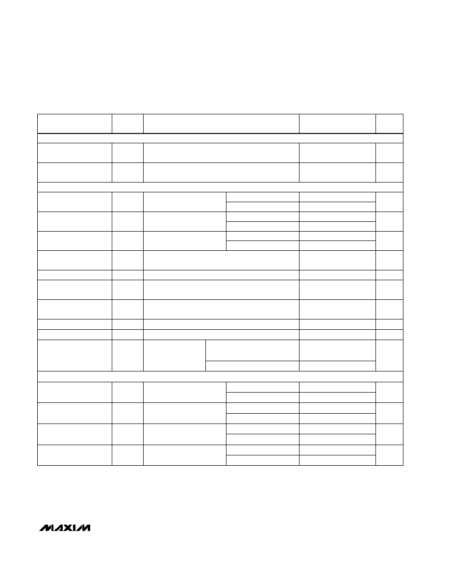
DG417/DG418/DG419
Improved, SPST/SPDT Analog Switches
_______________________________________________________________________________________
3
ELECTRICAL CHARACTERISTICS--Dual Supplies (continued)
(V+ = +15V, V- = -15V, V
L
= 5V, GND = 0V, V
INL
= 0.8V, V
INH
= 2.4V, T
A
= T
MIN
to T
MAX
, unless otherwise noted.)
-5
5
T
A
= +25∞C
-5
5
V
D
= 0V, f = 1MHz, Figure 8,
T
A
= +25∞C
V
IN
= 2.4V
T
A
= T
MIN
to T
MAX
V+ = 16.5V, V- = -16.5V,
V
IN
= 0V or 5V
T
A
= +25∞C
T
A
= T
MIN
to T
MAX
µA
-1
-0.0001
1
I-
Negative Supply Current
pF
8
C
S (OFF)
-5
5
T
A
= +25∞C
µA
T
A
= T
MIN
to T
MAX
V+ = 16.5V, V- = -16.5V,
V
IN
= 0V or 5V
µA
-1
-0.0001
1
I
L
Logic Supply Current
-5
5
T
A
= +25∞C
T
A
= T
MIN
to T
MAX
V+ = 16.5V, V- = -16.5V,
V
IN
= 0V or 5V
µA
-1
-0.0001
1
I
GND
Ground Current
-0.5
0.005
0.5
I
INH
DG417/DG418,
V
D
= ±10V, Figure 2
ns
100
175
Turn-On Time
Logic Input Current with
Input Voltage High
t
ON
V
IN
= 0.8V
µA
-0.5
0.005
0.5
I
INL
Logic Input Current with
Input Voltage Low
T
A
= +25∞C
DG417/DG418,
V
D
= ±10V, Figure 2
250
T
A
= T
MIN
to T
MAX
ns
V
GEN
= 0V, Figure 5, T
A
= +25∞C
pC
3
10
Q
Charge Injection (Note 3)
60
145
Turn-Off Time
t
OFF
T
A
= +25∞C
210
T
A
= T
MIN
to T
MAX
DG419,
V
S
= ±10V, Figure 3
ns
175
Transition Time
Source Off-Capacitance
CONDITIONS
UNITS
t
TRANS
35
MIN
TYP
MAX
(Note 2)
SYMBOL
T
A
= +25∞C
250
T
A
= T
MIN
to T
MAX
PARAMETER
DG419, V
S1
= V
S2
= ±10V
,
Figure 4, T
A
= +25∞C
ns
5
13
Break-Before-Make
Interval
t
D
R
L
= 500
, C
L
= 5pF, f = 1MHz, Figure 6, T
A
= +25∞C
dB
68
OIRR
Off-Isolation
Rejection Ratio (Note 6)
DG419, R
L
= 50
, C
L
= 5pF, f = 1MHz, Figure 7,
T
A
= +25∞C
dB
85
Crosstalk (Note 7)
V+ = 16.5V, V- = -16.5V,
V
IN
= 0V or 5V
µA
-1
-0.0001
1
I+
Positive Supply Current
V
D
= 0V, f = 1MHz, Figure 8,
T
A
= +25∞C
pF
8
C
D (OFF)
Drain Off-Capacitance
V
S
= 0V, f = 1MHz,
Figure 9,
T
A
= +25∞C
pF
30
C
D (ON)
or
C
S (ON)
Drain-Source
On-Capacitance
LOGIC INPUT
SUPPLY
DYNAMIC
DG417/DG418
DG419
DG417/DG418/DG419
Improved, SPST/SPDT Analog Switches
4
_______________________________________________________________________________________
ELECTRICAL CHARACTERISTICS--Single Supply
(V+ = +12V, V- = 0V, VL = 5V, GND = 0V, V
INH
= 2.4V, V
INL
= 0.8V, T
A
= +25∞C, unless otherwise noted.)
Note 2:
Typical values are for
design aid only
, are not guaranteed, and are not subject to production testing. The algebraic
convention where the most negative value is a minimum and the most positive value a maximum is used in this data sheet.
Note 3:
Guaranteed by design.
Note 4:
On-resistance match between channels and flatness is guaranteed only with bipolar-supply operation. Flatness is defined as
the difference between the maximum and the minimum value of on-resistance as measured at the extremes of the specified
analog range.
Note 5:
Leakage parameters I
S(OFF)
, I
D(OFF)
, and I
D(ON)
are 100% tested at the maximum rated hot temperature and guaranteed by
correlation at +25∞C.
Note 6:
Off-Isolation Rejection Ratio = 20log (V
D
/V
S
), V
D
= output, V
S
= input to off switch.
Note 7:
Between any two switches.
Drain-Source On-Resistance
R
DS(ON)
ns
ns
110
Turn-On Time
t
ON
DG417/DG418, V
D
= 8V, Figure 2
t
OFF
Charge Injection (Note 3)
Q
Turn-Off Time
DG417/DG418, V
D
= 8V, Figure 2
pC
40
µA
ns
60
Break-Before-Make Interval
t
D
DG419, R
L
= 1000
, C
L
= 35pF, Figure 4
2
10
C
L
= 10nF, V
GEN
= 0V, R
GEN
= 0V, Figure 5
-0.0001
Logic Supply Current
I
L
All channels on or off, V
L
= 5.25V,
V
IN
= 0V or 5V
µA
-0.0001
Negative Supply Current
I-
µA
-0.0001
Positive Supply Current
I+
All channels on or off, V+ = 13.2V,
V
L
= 5.25V, V
IN
= 0V or 5V
I
S
= -10mA, V
D
= 3.8V, V+ = 10.8V
40
100
All channels on or off, V+ = 13.2V,
V
L
= 5.25V, V
IN
= 0V or 5V
µA
-0.0001
Ground Current
I
GND
All channels on or off, V
L
= 5.25V,
V
IN
= 0V or 5V
CONDITIONS
UNITS
MIN
TYP
MAX
(Note 2)
SYMBOL
PARAMETER
(Note 3)
V
0
12
V
ANALOG
Analog Signal Range
SWITCH
DYNAMIC
SUPPLY
DG417/DG418/DG419
Improved, SPST/SPDT Analog Switches
_______________________________________________________________________________________
5
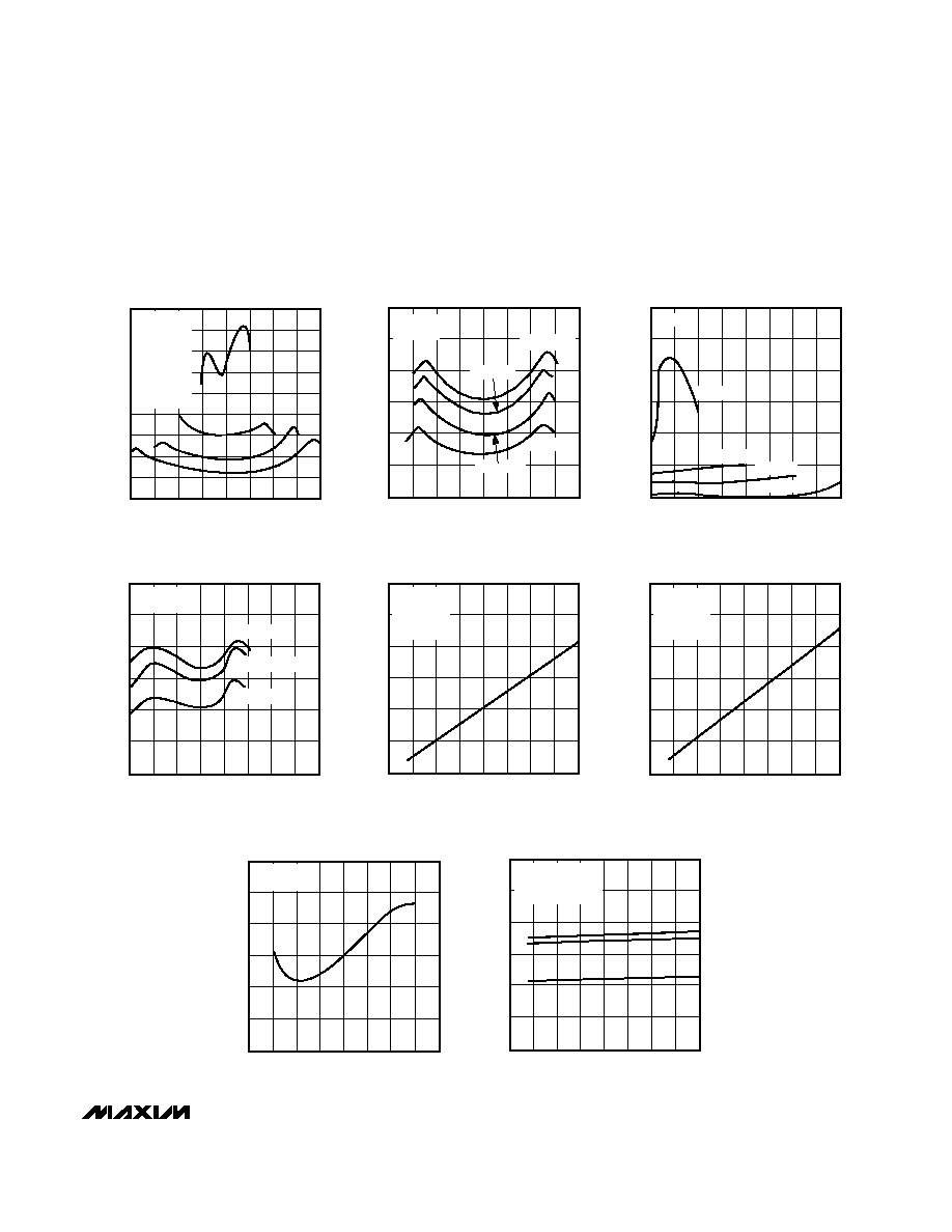
__________________________________________Typical Operating Characteristics
(T
A
= +25∞C, unless otherwise noted.)
45
5
-20
-10
10
ON-RESISTANCE vs. V
D
AND
POWER-SUPPLY VOLTAGE
15
35
DG417-01
V
D
(V)
R
DS(ON)
(
)
0
20
25
40
10
30
20
50
A
B
C
D
A: V+ = 5V,
V- = -5V
B: V+ = 10V,
V- = -10V
C: V+ = 15V,
V- = -15V
D: V+ = 20V,
V- = -20V
5
-20
-10
10
ON-RESISTANCE vs. V
D
AND
TEMPERATURE
30
DG417-02
V
D
(V)
R
DS(ON)
(
)
0
20
20
10
25
15
35
V+ = 15V
V- = -15V
T
A
= +125∞C
T
A
= +85∞C
T
A
= +25∞C
T
A
= -55∞C
20
0
5
15
ON-RESISTANCE vs. V
D
(SINGLE SUPPLY)
120
DG417-03
V
D
(V)
R
DS(ON)
(
)
10
20
80
40
100
60
140
V- = 0V
V+ = 5V
V+ = 10V
V+ = 15V
V+ = 20V
10
0
5
15
ON-RESISTANCE vs. V
D
AND
TEMPERATURE
60
DG417-04
V
D
(V)
R
DS(ON)
(
)
10
20
40
20
50
30
70
V+ = 12V
V- = 0V
T
A
= +125∞C
T
A
= +85∞C
T
A
= +25∞C
-60
-20
CHARGE INJECTION vs.
ANALOG VOLTAGE
40
DG417-07
V
D
(V)
Q (pC)
0
20
0
-40
20
-20
60
-15 -10
-5
5
10
15
V+ = 15V
V- = -15V
0.0001
-75
OFF-LEAKAGE CURRENT vs.
TEMPERATURE
10
DG417-05
TEMPERATURE (∞C)
OFF-LEAKAGE (nA)
25
125
0.1
0.001
1
0.01
100
V+ = 16.5V
V- = -16.5V
V
D
= ±15V
V
S
= 15V
±
0.0001
-75
ON-LEAKAGE CURRENT vs.
TEMPERATURE
10
DG417-06
TEMPERATURE (∞C)
ON-LEAKAGE (nA)
25
125
0.1
0.001
1
0.01
100
V+ = 16.5V
V- = -16.5V
V
D
= ±15V
V
S
= ±15V
0.0001
-75
SUPPLY CURRENT vs.
TEMPERATURE
10
DG417-08
TEMPERATURE (∞C)
I+, I-, I
L
(
µ
A)
25
125
0.1
0.001
1
0.01
100
A: I+ at V+ = 16.5V
B: I- at V- = -16.5V
C: I
L
at V
L
= 5V
A
B
C
DG417/DG418/DG419
__________Applications Information
Operation with Supply Voltages
Other than ±15V
Using supply voltages other than ±15V reduces the
analog signal range. The DG417/DG418/DG419 switch-
es operate with ±4.5V to ±20V bipolar supplies or with
a +10V to +30V single supply; connect V- to 0V when
operating with a single supply. Also, all device types
can operate with unbalanced supplies, such as +24V
and -5V. VL must be connected to +5V to be TTL com-
patible, or to V+ for CMOS-logic level inputs. The
Typical Operating Characteristics graphs show typical
on-resistance with ±20V, ±15V, ±10V, and ±5V sup-
plies. (Switching times increase by a factor of two or
more for operation at ±5V.)
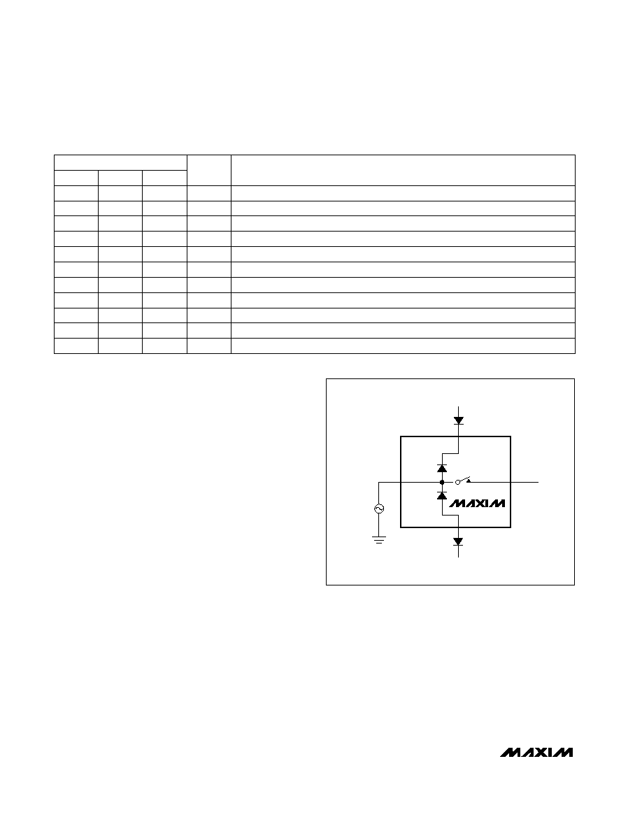
Overvoltage Protection
Proper power-supply sequencing is recommended for
all CMOS devices. Do not exceed the absolute maxi-
mum ratings because stresses beyond the listed rat-
ings may cause permanent damage to the devices.
Always sequence V+ on first, followed by VL, V-, and
logic inputs. If power-supply sequencing is not possi-
ble, add two small, external signal diodes in series with
the supply pins for overvoltage protection (Figure 1).
Adding diodes reduces the analog signal range to 1V
below V+ and 1V above V-, without affecting low switch
resistance and low leakage characteristics. Device
operation is unchanged, and the difference between
V+ and V- should not exceed +44V.
Improved, SPST/SPDT Analog Switches
6
_______________________________________________________________________________________
______________________________________________________________Pin Description
FUNCTION
DG417
DG418
1
--
Analog-Switch Source Terminal (normally closed)
PIN
--
1
Analog-Switch Source Terminal (normally open)
2
2
No Internal Connection
6
6
Logic-Level Input
5
5
Logic-Level Positive Supply Input
4
4
Analog-Signal Positive Supply Input
3
3
Logic Ground
7
7
Analog-Signal Negative Supply Input
V+
D
V-
S
V
g
DG41_
Figure 1. Overvoltage Protection Using External Blocking Diodes
NAME
DG419
--
S
--
S
--
N.C.
6
IN
5
VL
4
V+
3
GND
7
V-
8
8
Analog-Switch Drain Terminal
1
D
--
--
Analog-Switch Source Terminal 1 (normally closed)
2
S1
--
--
Analog-Switch Source Terminal 2 (normally open)
8
S2
DG417/DG418/DG419
Improved, SPST/SPDT Analog Switches
_______________________________________________________________________________________
7
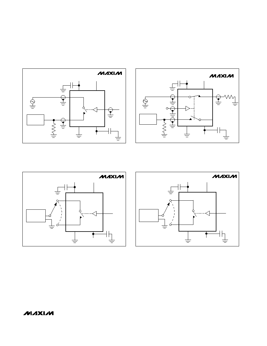
_____________________________________________________Test Circuits/Timing Diagrams
t
R
< 20ns
t
F
< 20ns
50%
0V
LOGIC
INPUT
V-
-15V
R
L
300
S
GND
C
L
INCLUDES FIXTURE AND STRAY CAPACITANCE.
V
OUT
= V
D
(
R
L
)
R
L
+ R
DS(ON)
SWITCH
INPUT
IN
+3V
t
OFF
0V
D
SWITCH
OUTPUT
0.9 x V
OUT
0.9 x V
OUT
t
ON
V
OUT
SWITCH
OUTPUT
LOGIC
INPUT
LOGIC INPUT WAVEFORMS INVERTED FOR SWITCHES
THAT HAVE THE OPPOSITE LOGIC SENSE.
VL
V+
C
L
35pF
+5V
+15V
V
OUT
DG417
DG418
t
R
< 20ns
t
F
< 20ns
50%
0V
LOGIC
INPUT
V-
-15V
R
L
1000
D
GND
C
L
INCLUDES FIXTURE AND STRAY CAPACITANCE.
LOGIC
INPUT
S1
IN
t
TRANS
+3V
t
TRANS
V
OUT1
V+
S2
V
OUT
0.8 x V
OUT1
V
OUT2
0.8 x V
OUT2
SWITCH
OUTPUT
VL
DG419
+15V
+5V
C
L
35pF
Figure 2. DG417/DG418 Switching Time
Figure 3. DG419 Transition Time
DG417/DG418/DG419
Improved, SPST/SPDT Analog Switches
8
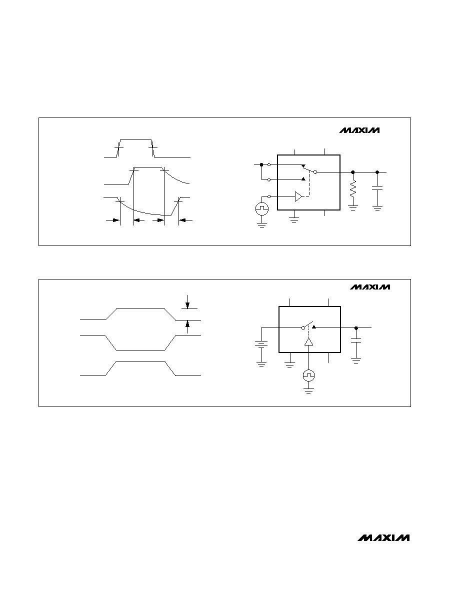
_______________________________________________________________________________________
50%
V
OUT1
V
OUT2
0.9 x V
OUT
+3V
0V
0V
LOGIC
INPUT
SWITCH
OUTPUT 1
SWITCH
OUTPUT 2
V
OUT
0.9 x V
OUT
t
D
t
D
LOGIC
INPUT
V-
-15V
R
L
300
GND
C
L
INCLUDES FIXTURE AND STRAY CAPACITANCE.
S2
D
IN1, IN2
VL
S1
V
OUT
V+
DG419
+5V
+15V
C
L
35pF
+10V
Figure 5. Charge Injection
V
GEN
GND
D
C
L
10nF
V
OUT
-15V
V-
V+
VL
V
OUT
IN
OFF
ON
OFF
V
OUT
Q =
V
OUT
x C
L
S
+5V
IN DEPENDS ON SWITCH CONFIGURATION;
INPUT POLARITY DETERMINED BY SENSE OF SWITCH.
OFF
ON
OFF
IN
V
IN
= +3V
DG417
DG418
DG419
+15V
Figure 4. DG419 Break-Before-Make Interval
______________________________________Test Circuits/Timing Diagrams (continued)
DG417/DG418/DG419
Improved, SPST/SPDT Analog Switches
_______________________________________________________________________________________
9
IN
0V or
2.4V
SIGNAL
GENERATOR 0dBm
+15V
10nF
VL
NETWORK
ANALYZER
S1 or S2
RL
GND
D
10nF
-15V
V-
V+
+5V
DG417
DG418
DG419
SIGNAL
GENERATOR 0dBm
+15V
V+
S2
RL
GND
D
V-
-15V
0V or 2.4V
IN
S1
50
VL
D
DG419
+5V
NETWORK
ANALYZER
10nF
10nF
CAPACITANCE
METER
S
D
GND
V-
-15V
IN
0V or
2.4V
+15V
VL
+5V
f = 1MHz
V+
DG417
DG418
DG419
10nF
10nF
S
D
GND
V-
-15V
IN
0V or
2.4V
+15V
VL
+5V
V+
DG417
DG418
DG419
CAPACITANCE
METER
f = 1MHz
10nF
10nF
Figure 6. Off-Isolation Rejection Ratio
Figure 7. DG419 Crosstalk
Figure 8. Drain-Source Off-Capacitance
Figure 9. Drain-Source On-Capacitance
______________________________________Test Circuits/Timing Diagrams (continued)
DG417/DG418/DG419
Improved, SPST/SPDT Analog Switches
10
______________________________________________________________________________________
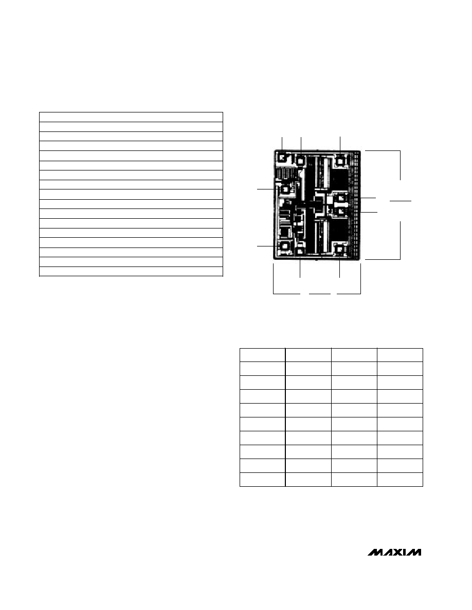
______________________Chip Topography
7
6
4
5
8
9
3
2
1
0.058"
1.47mm
0.076"
1.93mm
__Ordering Information (continued)
TRANSISTOR COUNT: 32
SUBSTRATE CONNECTED TO V+
* Contact factory for dice specifications.
**Contact factory for availability and processing to MIL-STD-883B.
PART
TEMP. RANGE
PIN-PACKAGE
DG417DK
DG417AK
-55∞C to +125∞C
-40∞C to +85∞C
8 CERDIP
8 CERDIP**
DG418
CJ
DG418CY
DG418C/D
0∞C to +70∞C
0∞C to +70∞C
0∞C to +70∞C
8 Plastic DIP
8 SO
Dice*
DG418DJ
DG418DY
-40∞C to +85∞C
-40∞C to +85∞C
8 Plastic DIP
8 SO
DG418DK
DG418AK
-55∞C to +125∞C
-40∞C to +85∞C
8 CERDIP
8 CERDIP**
DG419DK
DG419AK
-55∞C to +125∞C
-40∞C to +85∞C
8 CERDIP
8 CERDIP**
DG419
CJ
DG419CY
DG419C/D
0∞C to +70∞C
0∞C to +70∞C
0∞C to +70∞C
8 Plastic DIP
8 SO
Dice*
DG419DJ
DG419DY
-40∞C to +85∞C
-40∞C to +85∞C
8 Plastic DIP
8 SO
DG419
S
GND
V+
VL
IN
V-
S
D
D
DG418
N.C.
GND
V+
VL
IN
V-
S
D
N.C.
DG417
DIE PAD
1
2
D
3
4
5
6
GND
7
8
9
V+
VL
IN
V-
N.C.
N.C.
S

DG417/DG418/DG419
Improved, SPST/SPDT Analog Switches
______________________________________________________________________________________
11
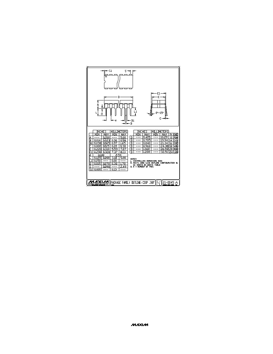
________________________________________________________Package Information
PDIPN.EPS
SOICN.EPS
Maxim cannot assume responsibility for use of any circuitry other than circuitry entirely embodied in a Maxim product. No circuit patent licenses are
implied. Maxim reserves the right to change the circuitry and specifications without notice at any time.
12
__________________Maxim Integrated Products, 120 San Gabriel Drive, Sunnyvale, CA 94086 (408) 737-7600
© 1996 Maxim Integrated Products
Printed USA
is a registered trademark of Maxim Integrated Products.
DG417/DG418/DG419
Improved, SPST/SPDT Analog Switches
Maxim cannot assume responsibility for use of any circuitry other than circuitry entirely embodied in a Maxim product. No circuit patent licenses are
implied. Maxim reserves the right to change the circuitry and specifications without notice at any time.
12
__________________Maxim Integrated Products, 120 San Gabriel Drive, Sunnyvale, CA 94086 (408) 737-7600
© 1996 Maxim Integrated Products
Printed USA
is a registered trademark of Maxim Integrated Products.
___________________________________________Package Information (continued)
CDIPS.EPS