 | –≠–ª–µ–∫—Ç—Ä–æ–Ω–Ω—ã–π –∫–æ–º–ø–æ–Ω–µ–Ω—Ç: DG421DJ | –°–∫–∞—á–∞—Ç—å:  PDF PDF  ZIP ZIP |
DG421/DG423/DG425
Improved Low-Power,
CMOS Analog Switches with Latches
________________________________________________________________
Maxim Integrated Products
1
TOP VIEW
16
15
14
13
12
11
10
9
1
2
3
4
5
6
7
8
S1
IN1
V-
GND
N.C.
N.C.
WR
D1
DG421
V
L
V+
IN2
S2
D2
RS
N.C.
N.C.
DIP
_________________Pin Configurations
SWITCHES SHOWN FOR
LOGIC "1" INPUT
D2
D1
CK
R
D
Q
CK
R
D
Q
TWO SPST SWITCHES
PER PACKAGE
WR RS IN
SWITCH
0
1
0
1
Off
On
LOGIC "O"
0.8V
LOGIC "1"
2.4V
DG421 TRUTH TABLE
S1
WR
IN1
IN2
RS
S2
DG421
__Functional Diagrams/Truth Tables
Call toll free 1-800-998-8800 for free samples or literature.
19-0137; Rev 1; 3/94
_______________General Description
Maxim's redesigned DG421/DG423/DG425 monolithic
analog switches now feature guaranteed on-resistance
matching (3
max) between switches and on-resistance
flatness over the signal range (4
max). These low on-
resistance switches (20
typ) conduct equally well in both
directions. They guarantee a low charge injection of 15pC
maximum and an ESD tolerance of 2000V minimum per
Method 3015.7. Off leakage current over temperature has
also been reduced (less than 5nA at +85∞C).
The DG421/DG423/DG425 are precision, dual CMOS
switches with latchable logic inputs that simplify inter-
facing with microprocessors (µPs). The single-pole/single-
throw DG421 and double-pole/single-throw DG425 are
normally open dual switches. The dual, single-
pole/double-throw DG423 has two normally open and
two normally closed switches. Fast switching times
(175ns for t
ON
and 145ns for t
OFF
) and low power
consumption (35µW max) make these parts ideal for
battery-powered applications requiring µP-compatible
switches. Operation is from a single +10V to +30V supply,
or bipolar ±4.5V to ±20V supplies. Fabricated with the
same 44V silicon-gate process, these switches have
rail-to-rail signal handling capabilities.
_______________________Applications
Sample-and-Hold Circuits
Modems
Fax Machines
Test Equipment
Battery-Operated Systems
PBX, PABX
Guidance and Control Systems
Military Radios
Audio Signal Routing
Communication Systems
______________________New Features
o
Plug-In Upgrades for Industry-Standard
DG421/DG423/DG425
o
Improved r
(DS)ON
Match Between Channels (3
max)
o
Guaranteed r
FLAT(ON)
Over Signal Range (4
max)
o
Improved Charge Injection (15pC max)
o
Improved Off Leakage Current Over Temperature
(<5nA at +85∞C)
o
Withstands Electrostatic Discharge (2000V min)
per Method 3015.7
__________________Existing Features
o
Low r
DS(ON)
(35
max)
o
Single-Supply Operation +10V to +30V
Bipolar-Supply Operation ±4.5V to ±20V
o
Low Power Consumption (35µW max)
o
Rail-to-Rail Signal Handling Capability
o
TTL/CMOS-Logic Compatible
______________Ordering Information
Ordering Information continued at end of data sheet.
* Contact factory for dice specifications.
**Contact factory for availability and processing to MIL-STD-883B.
Functional Diagrams/Truth Tables continued at end of data sheet.
N.C. = No Internal Connection
Pin Configurations continued at end of data sheet.
16 CERDIP**
-55∞C to +125∞C
DG421AK
16 SO
-40∞C to +85∞C
DG421DY
Dice*
0∞C to +70∞C
DG421C/D
0∞C to +70∞C
16 CERDIP
-40∞C to +85∞C
DG421DK
16 Plastic DIP
-40∞C to +85∞C
DG421DJ
16 SO
0∞C to +70∞C
DG421CY
16 Plastic DIP
DG421
CJ
PIN-PACKAGE
TEMP. RANGE
PART
DG421/DG423/DG425
Improved Low-Power,
CMOS Analog Switches with Latches
2
_______________________________________________________________________________________
Voltage Referenced to V-
V+ . . . . . . . . . . . . . . . . . . . . . . . . . . . . . . . . . . . . . . . . . . . . . . . . . . . . . . . . . . . . 44V
GND . . . . . . . . . . . . . . . . . . . . . . . . . . . . . . . . . . . . . . . . . . . . . . . . . . . . . . . . . 25V
V
L
. . . . . . . . . . . . . . . . . . . . . . . . . . . . . . . . . . (GND - 0.3V) to (V+ + 0.3V)
Digital Inputs, V
S
, V
D
(Note 1) . . . . . . . . . . . . . . (V- - 2V) to (V+ + 2V)
Current (any terminal, except S or D) .................................30mA
Continuous Current, S or D .................................................20mA
Peak Current, S or D (pulsed at 1ms, 10% duty cycle max)...100mA
Continuous Power Dissipation (T
A
= +70∞C)
16-Pin Plastic DIP (derate 10.53mW/∞C above +70∞C) . . .842mW
20-Pin PLCC (derate 10.00mW/∞C above +70∞C) . . . . . 800mW
16-Pin CERDIP (derate 10.00mW/∞C above +70∞C) . . . 800mW
Operating Temperature Ranges
DG42_C_ . . . . . . . . . . . . . . . . . . . . . . . . . . . . . . . . . . . . . . . . . . 0∞C to +70∞C
DG42_D_ . . . . . . . . . . . . . . . . . . . . . . . . . . . . . . . . . . . . . . . -40∞C to +85∞C
DG42_A_ . . . . . . . . . . . . . . . . . . . . . . . . . . . . . . . . . . . . . . -55∞C to +125∞C
Storage Temperature Ranges
DG42_C_/DG42_D_ . . . . . . . . . . . . . . . . . . . . . . . . . . . -65∞C to +125∞C
DG42_A_ . . . . . . . . . . . . . . . . . . . . . . . . . . . . . . . . . . . . . -65∞C to +150∞C
Lead Temperature (soldering, 10sec). . . . . . . . . . . . . . . . . . . . +300∞C
ELECTRICAL CHARACTERISTICS
(V+ = 15V, V- = -15V, V
L
= +5V, GND = 0V, V
INH
= +2.4V, V
INL
= +0.8V, T
A
= T
MIN
to T
MAX
, unless otherwise noted.)
Stresses beyond those listed under "Absolute Maximum Ratings" may cause permanent damage to the device. These are stress ratings only, and functional
operation of the device at these or any other conditions beyond those indicated in the operational sections of the specifications is not implied. Exposure to
absolute maximum rating conditions for extended periods may affect device reliability.
ABSOLUTE MAXIMUM RATINGS
Note 1:
Signals on S, D, or IN exceeding V+ or V- are clamped by internal diodes. Limit forward current to maximum current ratings.
T
A
= +25∞C
T
A
= T
MIN
to T
MAX
V+ = 13.5V,
V- = -13.5V,
I
S
= -10mA,
V
D
= ±10V
r
DS(ON)
Drain-Source
On-Resistance
CONDITIONS
SYMBOL
PARAMETER
20
45
DG42_C, DG42_D
MIN
TYP
MAX
(Note 2)
UNITS
45
45
20
35
DG42_A
MIN
TYP
MAX
(Note 2)
T
A
= +25∞C
T
A
= T
MIN
to T
MAX
V+ = 16.5V,
V- = -16.5V,
I
S
= -10mA,
V
D
= ±10V
r
DS(ON)
On-Resistance Match
Between Channels
(Note 4)
4
4
3
3
T
A
= +25∞C
T
A
= T
MIN
to T
MAX
V+ = 15V,
V- = -15V,
I
S
= -10mA,
V
D
= ±5V
r
FLAT(ON)
On-Resistance
Flatness (Note 4)
5
5
4
4
(Note 3)
V
ANALOG
Analog Signal Range
V
-15
15
-15
15
T
A
= +25∞C
T
A
= T
MIN
to T
MAX
V+ = 16.5V,
V- = -16.5V,
V
D
= ±15.5V,
V
S
=
15.5V
m
I
S(OFF)
Source-Off
Leakage Current
(Note 5)
nA
-5
5
-10
10
-0.50
-0.01
0.50
-0.25
-0.01
0.25
T
A
= +25∞C
T
A
= T
MIN
to T
MAX
V+ = 16.5V,
V- = -16.5V,
V
D
= ±15.5V,
V
S
=
15.5V
m
I
D(OFF)
Drain-Off
Leakage Current
(Note 5)
nA
-5
5
-10
10
-0.50
-0.01
0.50
-0.25
-0.01
0.25
T
A
= +25∞C
T
A
= T
MIN
to T
MAX
V+ = 16.5V,
V- = -16.5V,
V
D
= ±15.5V,
V
S
= ±15.5V
I
D(ON)
Drain-On
Leakage Current
(Note 5)
nA
-10
10
-20
20
-1.0
-0.04
1.0
-0.40
-0.04
0.40
SWITCH

DG421/DG423/DG425
Improved Low-Power,
CMOS Analog Switches with Latches
_______________________________________________________________________________________
3
ELECTRICAL CHARACTERISTICS (continued)
(V+ = 15V, V- = -15V, V
L
= +5V, GND = 0V, V
INH
= +2.4V, V
INL
= +0.8V, T
A
= T
MIN
to T
MAX
, unless otherwise noted.)
T
A
= +25∞C
T
A
= T
MIN
to T
MAX
All channels on or off,
V+ = 16.5V, V- = -16.5V,
V
IN
= 0V or 5V
I+
Positive Supply Current
CONDITIONS
SYMBOL
PARAMETER
µA
UNITS
-5.0
5.0
-1.0
0.01
1.0
MIN
TYP
MAX
(Note 2)
IN = 2.4V, all others = 0.8V
I
INH
Input Current with Input Voltage High
µA
-0.50
0.005
0.50
IN = 0.8V, all others = 2.4V
I
INL
Input Current with Input Voltage Low
µA
-0.50
0.005
0.50
(Note 3)
V+, V-
Power Supply Range
V
±4.5
±20
T
A
= +25∞C
T
A
= T
MIN
to T
MAX
All channels on or off,
V+ = 16.5V, V- = -16.5V,
V
IN
= 0V or 5V
I-
Negative Supply Current
µA
-5.0
5.0
-1.0
-0.01
1.0
T
A
= +25∞C
T
A
= T
MIN
to T
MAX
All channels on or off,
V+ = 16.5V, V- = -16.5V,
V
IN
= 0V or 5V
I
GND
Ground Current
µA
-5.0
5.0
-1.0
-0.01
1.0
T
A
= +25∞C
T
A
= T
MIN
to T
MAX
Figure 2
t
ON
Turn-On Time
ns
300
150
250
200
ns
Figure 2
t
OFF
Turn-Off Time
T
A
= +25∞C
T
A
= -55∞C to +125∞C
V
S
= ±10V,
R
L
= 300
,
C
L
= 35pF,
Figure 3
t
WW
Latch Timing
ns
200
200
T
A
= +25∞C
T
A
= -55∞C to +125∞C
t
DW
100
100
T
A
= +25∞C
T
A
= -55∞C to +125∞C
t
WD
100
60
T
A
= +25∞C
5
25
T
A
= +25∞C
T
A
= T
MIN
to T
MAX
All channels on or off,
V+ = 16.5V, V- = -16.5V,
V
IN
= 0V or 5V
I
L
Logic Supply Current
µA
-5.0
5.0
-1.0
-0.01
1.0
Break-Before-Make Interval (Note 3)
t
D
DG423, Figure 4
ns
T
A
= +25∞C
10
15
Charge Injection (Note 3)
Q
C
L
= 10nF, V
G
= 0V,
R
G
= 0
, Figure 5
pC
T
A
= +25∞C
72
Off-Isolation Rejection Ratio
(Note 6)
OIRR
R
L
= 100
, C
L
= 5pF,
f = 1MHz, Figure 6
dB
T
A
= +25∞C
12
Drain-Off Capacitance
C
D(OFF)
f = 1MHz, Figure 8
pF
T
A
= +25∞C
90
Crosstalk (Note 7)
R
L
= 50
, C
L
= 5pF,
f = 1MHz, Figure 7
dB
T
A
= +25∞C
12
Source-Off Capacitance
C
S(OFF)
f = 1MHz, Figure 8
pF
Note 2:
Typical values are
for design aid only
, are not guaranteed, and are not subject to production testing. The algebraic convention,
where the most negative value is a minimum and the most positive value a maximum, is used in this data sheet.
Note 3:
Guaranteed by design.
Note 4:
On-resistance match between channels and flatness are guaranteed only with bipolar-supply operation. Flatness is defined as the dif-
ference between the maximum and minimum value of on-resistance as measured at the extremes of the specified analog signal range.
Note 5:
Leakage parameters I
S(OFF)
, I
D(OFF)
, and I
D(ON)
are 100% tested at the maximum rated hot temperature and guaranteed by
correlation at +25∞C.
Note 6:
Off-Isolation Rejection Ratio = 20log (V
D
/V
S
), V
D
= output, V
S
= input to off switch.
Note 7:
Between any two switches.
T
A
= +25∞C
39
Drain-On Capacitance
C
D(ON)
f = 1MHz, Figure 9
pF
T
A
= +25∞C
39
Source-On Capacitance
C
S(ON)
f = 1MHz, Figure 9
pF
INPUT
SUPPLY
DYNAMIC
DG421/DG423/DG425
Improved Low-Power,
CMOS Analog Switches with Latches
4
_______________________________________________________________________________________
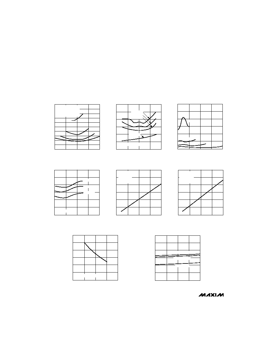
50
55
20
-20
ON-RESISTANCE vs. V
D
(DUAL-SUPPLIES)
25
45
MAX401-1
V
D
(V)
r
DS
(ON)
(
)
10
35
30
-10
0
20
40
15
10
5
A: V+ = 5V, V- = -5V
B: V+ = 10V, V- = -10V
C: V+ = 15V, V- = -15V
D: V+ = 20V, V- = -20V
A
B
C
D
35
5
-20
ON-RESISTANCE vs. V
D
AND
TEMPERATURE (DUAL SUPPLIES)
10
30
MAX401-2
V
D
(V)
r
DS
(ON)
(
)
20
20
15
-10
10
25
0
V+ = 15V, V- = -15V
T
A
= +125∞C
T
A
= +85∞C
T
A
= +25∞C
T
A
= -55∞C
140
20
0
ON-RESISTANCE vs. V
D
(SINGLE SUPPLY)
40
120
MAX401-3
V
D
(V)
r
DS
(ON)
(
)
20
80
60
5
15
100
10
V+ = 5V
V- = 0V
V+ = 10V
V+ = 15V
V+ = 20V
70
10
0
ON-RESISTANCE vs. V
D
AND
TEMPERATURE (SINGLE SUPPLY)
20
60
MAX401-4
V
D
(V)
r
DS
(ON)
(
)
20
40
30
5
15
50
10
V+ = 12V, V- = 0V
T
A
= +125∞C
T
A
= +85∞C
T
A
= +25∞C
100
0.0001
-75
125
OFF LEAKAGE CURRENTS vs.
TEMPERATURE
0.001
10
MAX401-5
TEMPERATURE (∞C)
OFF LEAKAGE (nA)
0.1
0.01
25
1
V+ = 16.5V
V- = -16.5V
V
D
= ±15V
V
S
= ±15V
100
0.0001
-75
125
ON LEAKAGE CURRENTS vs.
TEMPERATURE
0.001
10
MAX401-6
TEMPERATURE (∞C)
ON LEAKAGE (nA)
0.1
0.01
25
1
V+ = 16.5V
V- = -16.5V
V
D
= ±15V
V
S
= ±15V
60
-60
-20
20
CHARGE INJECTION vs.
ANALOG VOLTAGE
-40
40
MAX401-7
V
D
(V)
Q (pC)
10
0
-20
-10
0
20
V+ = 15V, V- = -15V
100
0.0001
-75
125
SUPPLY CURRENT vs.
TEMPERATURE
0.001
10
MAX401-8
TEMPERATURE (∞C)
I+, I-, I
L
(
µ
A)
0.1
0.01
25
1
I+ at V+ = 16.5V
I- at V- = -16.5V
I
L
at V
L
= 5V
__________________________________________Typical Operating Characteristics
(T
A
= +25∞C, unless otherwise noted.)

DG421/DG423/DG425
Improved Low-Power,
CMOS Analog Switches with Latches
_______________________________________________________________________________________
5
___________________Pin Descriptions
1, 8
D1, D2
Drain Terminals
2
≠
W
≠
--
≠
R
≠
Write Select
3, 4, 5, 6
N.C.
No Internal Connection
7
≠
R
≠
--
≠
S
≠
Reset Select
9, 16
S1, S2
Source Terminals
10, 15
IN1, IN2
Input Control
11
V+
Positive Supply
12
V
L
Logic Supply
13
GND
Ground
14
V-
Negative Supply
1, 8, 3, 6
2, 10, 4, 8
Drain Terminals
2
3
Write Select
≠
W
≠
--
≠
R
≠
16, 9, 4, 5 20, 12, 5, 7
Source Terminals
S1-S4
7
9
Resets Select
D1-D4
15, 10
19, 13
Input Control
IN1, IN2
11
14
Positive Supply
V+
≠
R
≠
--
≠
S
≠
12
15
Logic Supply
V
L
--
1, 6, 11, 16
No Internal Connection
N.C.
14
18
Negative Supply
V-
13
17
Ground
GND
PIN
NAME
FUNCTION
DIP
PLCC
FUNCTION
NAME
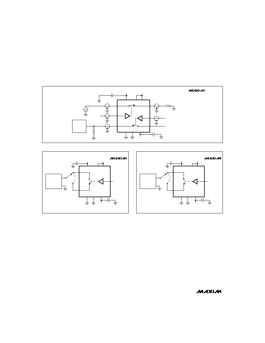
Figure 1. Overvoltage Protection Using External Blocking Diodes
__________Applications Information
Operation with Supply Voltages
Other Than ±15V
The DG421/DG423/DG425 switches operate with ±4.5V
to ±20V bipolar supplies or with a +10V to +30V single
supply. In either case, analog signals ranging from V+
to V- can be switched. The
Typical Operating
Characteristics graphs illustrate typical analog-signal
and supply-voltage on-resistance variations. The usual
on-resistance temperature coefficient is 0.5%/∞C (typ).
Logic Inputs
These devices operate with a single positive supply or
with bipolar supplies. They maintain TTL compatibility
with supplies anywhere in the ±4.5V to ±20V range as
long as V
L
= +5V. If V
L
is connected to V+ or another
supply at voltages other than +5V, the devices will
operate at CMOS-logic-level inputs.
Overvoltage Protection
Proper power-supply sequencing is recommended for
all CMOS devices. Do not exceed the absolute maxi-
mum ratings because stresses beyond the listed rat-
ings may cause permanent damage to the devices.
Always sequence V+ on first, followed by V
L
, V-, and
logic inputs. If power-supply sequencing is not possi-
ble, add two small, external signal diodes in series with
supply pins for overvoltage protection (Figure 1).
Adding diodes reduces the analog signal range to 1V
below V+ and 1V above V-, without affecting low switch
resistance and low leakage characteristics. Device
operation is unchanged, and the difference between V+
and V- should not exceed +44V.
V+
D
V-
S
V
g
DG421
DG423/DG425
DG421/DG423/DG425
Improved Low-Power,
CMOS Analog Switches with Latches
6
_______________________________________________________________________________________
D
-15V
( )
V-
R
L
V
OUT
V+
+15V
+5V
V
L
GND
V
D
= 10V for t
ON
V
D
= -10V for t
OFF
IN
LOGIC
INPUT
REPEAT TEST FOR IN2 AND S2.
C
L
INCLUDES FIXTURE AND STRAY CAPACITANCE.
C
L
SWITCH OUTPUT
S
LOGIC
INPUT
SWITCH
OUTPUT
t
R
< 20ns
t
F
< 20ns
V
OUT
t
OFF
50%
3V
0V
0V
NOTE:
LOGIC INPUT WAVEFORM IS INVERTED FOR
SWITCHES THAT HAVE THE OPPOSITE LOGIC SENSE.
DG421
DG423
DG425
V
OUT
= V
D
R
L
R
L
+ r
DS(ON)
0.9 x V
OUT
0.9 x V
OUT
-V
OUT
t
ON
*V
D
= 10V for t
ON
, V
D
= -10V for t
OFF
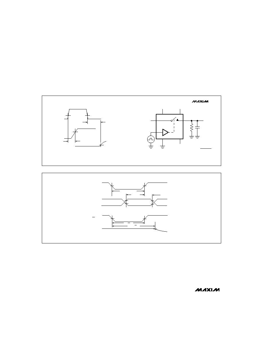
Figure 2. Switching Time
3V
0
3V
0
3V
0
V
OUT
0
WR
IN
RS
SWITCH
OUTPUT
1.5V
t
WW
t
DW
t
WD
2.0V
0.8V
1.5V
t
RS
t
OFF(RS)
0.8 x V
OUT
Figure 3. Latch Timing
V
OUT
is the steady-state output with the switch on. Feedthrough via switch capacitance may result in spikes at the
leading and trailing edge of the output waveform.
______________________________________________Timing Diagrams/Test Circuits

DG421/DG423/DG425
Improved Low-Power,
CMOS Analog Switches with Latches
_______________________________________________________________________________________
7
0FF
0N
0FF
V
OUT
IN
Q =
V
OUT
x C
L
IN DEPENDENT ON SWITCH CONFIGURATION.
INPUT POLARITY DETERMINED BY SENSE OF SWITCH.
V
OUT
DG421
DG423
DG425
R
g
-15V
V-
V
OUT
V+
+15V
+5V
V
g
GND
V
IN
= 3V
WR
D
C
L
10nF
RS V
L
S
IN
Figure 5. Charge Injection
_________________________________Timing Diagrams/Test Circuits (continued)
D
-15V
V-
R
L2
300
V
OUT1
V+
+15V
+5V
V
L
GND
V
D
= 10V
V
D
= 10V
LOGIC
INPUT
C
L
INCLUDES FIXTURE AND STRAY CAPACITANCE.
C
L2
35pF
S
LOGIC
INPUT
SWITCH
OUTPUT 1
SWITCH
OUTPUT 2
0.9 x V
OUT
V
OUT1
0.9 x V
OUT
t
D
50%
3V
0V
0V
0V
V
OUT2
t
D
D
R
L
= 1000
C
L
= 35pF
S
R
L1
300
C
L1
35pF
RS
V
OUT2
DG423
IN
WR
Figure 4. DG423 Break-Before-Make Interval
-15V
V-
R
L
GND
WR
SIGNAL GENERATOR
+15V
V+
10nF
RS
+5V
V
L
10nF
D
S
0V or 2.4V
IN
DG421
DG423
DG425
V
S
V
D
NETWORK
ANALYZER
Figure 6 . Off-Isolation Rejection Ratio
DG421/DG423/DG425
Improved Low-Power,
CMOS Analog Switches with Latches
8
_______________________________________________________________________________________
-15V
V-
GND
WR
+15V
V+
10nF
RS
+5V
V
L
10nF
D
S
0V or 2.4V
IN
CAPACITANCE
METER
DG421
DG423
DG425
Figure 8. Drain/Source-Off Capacitance
_________________________________Timing Diagrams/Test Circuits (continued)
-15V
V-
R
L
GND
WR
NETWORK
ANALYZER
SIGNAL GENERATOR
+15V
V+
10nF
RS
+5V
50
0V or 2.4V
0V or 2.4V
N.C.
V
L
10nF
D
IN
S
S
IN
DG421
DG423
DG425
D
Figure 7. Crosstalk
-15V
V-
GND
WR
+15V
V+
10nF
RS
+5V
V
L
10nF
D
S
0V or 2.4V
IN
CAPACITANCE
METER
DG421
DG423
DG425
Figure 9. Drain/Source-On Capacitance

DG421/DG423/DG425
Improved Low-Power,
CMOS Analog Switches with Latches
_______________________________________________________________________________________
9
_____________________________________________Pin Configurations (continued)
2
1
20
D3
S3
N.C.
S4
D4
18
17
16
15
14
WR
D1
N.C.
S1
IN1
4
5
6
7
8
V-
GND
N.C.
V
L
V+
RS
D2
N.C.
S2
IN2
3
19
13
9
10
11
12
DG423
DG425
PLCC
16
15
14
13
12
11
10
9
1
2
3
4
5
6
7
8
S1
IN1
V-
GND
S3
D3
WR
D1
DG423
DG425
V
L
V+
IN2
S2
D2
RS
D4
S4
DIP
_____________________________Functional Diagrams/Truth Tables (continued)
WR
RS
IN
SWITCH 1, 2
0
1
0
1
Off
On
LOGIC "O"
0.8V
LOGIC "1"
2.4V
DG423 TRUTH TABLE
D2
D1
CK
D
Q
TWO SPDT SWITCHES PER PACKAGE
S1
WR
IN1
IN2
RS
S2
DG423
S3
R
Q
CK
D
Q
R Q
S4
D3
D4
SWITCH 3, 4
On
Off
D2
D1
CK
D
TWO DPST SWITCHES PER PACKAGE
S1
WR
IN1
IN2
RS
S2
DG425
S3
R
Q
CK
D
R Q
S4
D3
D4
WR RS IN SWITCH
0
1
0
1
Off
On
LOGIC "O"
0.8V
LOGIC "1"
2.4V
DG425 TRUTH TABLE
LATCH OPERATION TRUTH TABLE
WR
RS
IN
X
1
X
1
LATCH/SWITCH X
X
X
0
0
X
X
Latch operation transparent.
Control data latched in.
Switches on or off as selected by last IN.
All latches reset. Switches on or off as
when IN = 0, WR = 0, RS = 1.
TOP VIEW
N.C. = No Internal Connection
DG421/DG423/DG425
Improved Low-Power,
CMOS Analog Switches with Latches
10
______________________________________________________________________________________
* Contact factory for dice specifications.
**Contact factory for availability and processing to MIL-STD-883B.
_Ordering Information (continued)
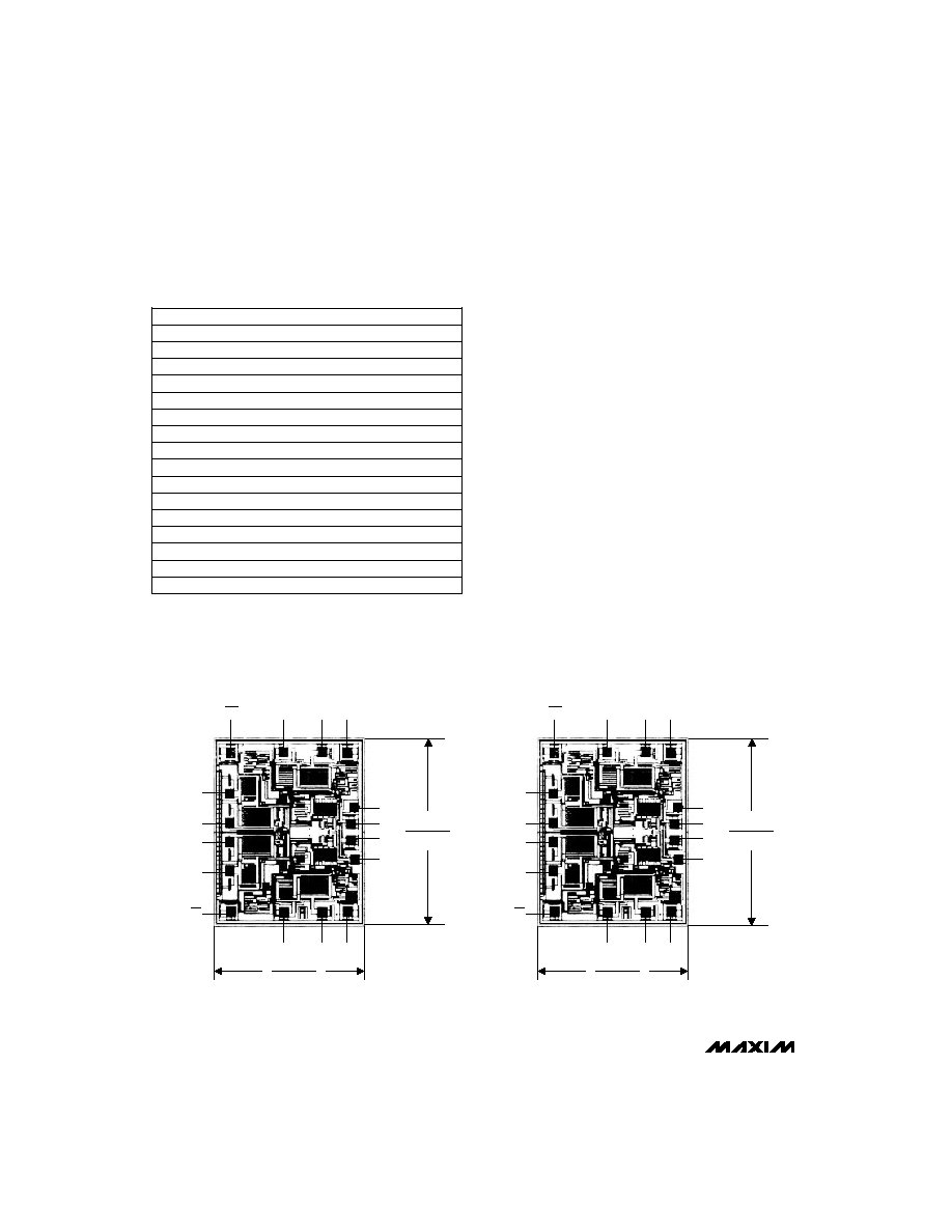
___________________________________________________________Chip Topographies
0.105"
(2.66mm)
0.082"
(2.08mm)
D1
S1
IN1
N.C.
N.C.
N.C.
N.C.
D2
RS
S2
IN2
V-
GND
VL
V+
WR
0.105"
(2.66mm)
0.082"
(2.08mm)
D1
S1
IN1
D3
S3
S4
D4
D2
RS
S2
IN2
V-
GND
VL
V+
WR
DG421
DG423
DG421
DG423/DG425
V
L
V
L
TRANSISTOR COUNT: 100
SUBSTRATE CONNECTED TO V+
TRANSISTOR COUNT: 100
SUBSTRATE CONNECTED TO V+
PART
TEMP. RANGE PIN-PACKAGE
DG423
CJ
0∞C to +70∞C
16 Plastic DIP
DG423CY
0∞C to +70∞C
16 SO
DG423DJ
-40∞C to +85∞C
16 Plastic DIP
DG423DN
-40∞C to +85∞C
20 PLCC
DG423AK
-55∞C to +125∞C
16 CERDIP**
DG425
CJ
0∞C to +70∞C
16 Plastic DIP
DG425CY
0∞C to +70∞C
16 SO
DG425DJ
-40∞C to +85∞C
16 Plastic DIP
DG425DN
-40∞C to +85∞C
20 PLCC
DG425AK
-55∞C to +125∞C
16 CERDIP**
DG423C/D
0∞C to +70∞C
Dice*
DG423DY
-40∞C to +85∞C
16 SO
DG423DK
-40∞C to +85∞C
16 CERDIP
DG425C/D
0∞C to +70∞C
Dice*
DG425DY
-40∞C to +85∞C
16 SO
DG425DK
-40∞C to +85∞C
16 CERDIP

DG421/DG423/DG425
Improved Low-Power,
CMOS Analog Switches with Latches
______________________________________________________________________________________
11
C
A
A2
E1
D
E
e
A
e
B
A3
B1
B
DIM
A
A1
A2
A3
B
B1
C
D
D1
E
E1
e
e
A
e
B
L
MIN
≠
0.015
0.125
0.055
0.016
0.050
0.008
0.745
0.005
0.300
0.240
≠
0.115
0∞
MAX
0.200
≠
0.150
0.080
0.022
0.065
0.012
0.765
0.030
0.325
0.280
0.400
0.150
15∞
MIN
≠
0.38
3.18
1.40
0.41
1.27
0.20
18.92
0.13
7.62
6.10
≠
2.92
0∞
MAX
5.08
≠
3.81
2.03
0.56
1.65
0.30
19.43
0.76
8.26
7.11
10.16
3.81
15∞
INCHES
MILLIMETERS
2.54 BSC
7.62 BSC
0.100 BSC
0.300 BSC
A1
L
D1
e
21-587A
16-PIN PLASTIC
DUAL-IN-LINE
PACKAGE
________________________________________________________Package Information
C
A
D
B1
B
DIM
A
B
B1
C
D
E
E1
e
L
L1
Q
S
S1
MIN
≠
0.014
0.038
0.008
≠
0.220
0.290
0.125
0.150
0.015
≠
0.005
0∞
MAX
0.200
0.023
0.065
0.015
0.840
0.310
0.320
0.200
≠
0.060
0.080
≠
15∞
MIN
≠
0.36
0.97
0.20
≠
5.59
7.37
3.18
3.81
0.38
≠
0.13
0∞
MAX
5.08
0.58
1.65
0.38
21.34
7.87
8.13
5.08
≠
1.52
2.03
≠
15∞
INCHES
MILLIMETERS
2.54 BSC
0.100 BSC
Q
L
S1
e
21-590B
16-PIN CERAMIC
DUAL-IN-LINE
PACKAGE
S
L1
E
E1
Maxim cannot assume responsibility for use of any circuitry other than circuitry entirely embodied in a Maxim product. No circuit patent licenses are
implied. Maxim reserves the right to change the circuitry and specifications without notice at any time.
12
__________________Maxim Integrated Products, 120 San Gabriel Drive, Sunnyvale, CA 94086 (408) 737-7600
© 1994 Maxim Integrated Products
Printed USA
is a registered trademark of Maxim Integrated Products.
DG421/DG423/DG425
Improved Low-Power,
CMOS Analog Switches with Latches
DIM
A
A1
A2
A3
B
B1
C
D
D1
D2
D3
e
MIN
0.165
0.100
0.145
0.020
0.013
0.026
0.009
0.385
0.350
0.290
MAX
0.180
0.110
0.156
≠
0.021
0.032
0.011
0.395
0.355
0.330
MIN
4.19
2.54
3.68
0.51
0.33
0.66
0.23
9.78
8.89
7.37
MAX
4.57
2.79
3.96
≠
0.53
0.81
0.28
10.03
9.02
8.38
INCHES
MILLIMETERS
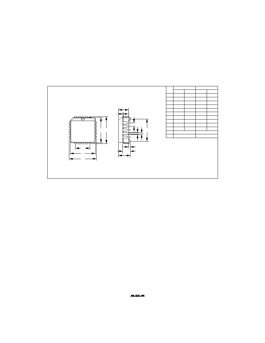
20-PIN PLASTIC
LEADED CHIP
CARRIER
PACKAGE
21-981A
D
D1
D
D1
D3
D2
e B1
B
A3
A
A1
A2
5.08 REF
0.200 REF
1.27 REF
0.050 REF
C
___________________________________________Package Information (continued)