 | –≠–ª–µ–∫—Ç—Ä–æ–Ω–Ω—ã–π –∫–æ–º–ø–æ–Ω–µ–Ω—Ç: DG529CJ | –°–∫–∞—á–∞—Ç—å:  PDF PDF  ZIP ZIP |
_______________General Description
Maxim's DG528/DG529 are monolithic, 8-channel,
CMOS multiplexers with on-board address and control
latches that simplify design and reduce board space in
microprocessor-based applications. The DG528 is a
single-ended, 1-of-8 multiplexer, while the DG529 is a
differential, 2-of-8 multiplexer. These devices can oper-
ate as multiplexers or demultiplexers.
The DG528/DG529 have break-before-make switching
to prevent momentary shorting of the input signals.
Each device operates with dual supplies (±4.5V to
±20V) or a single supply (+5V to +30V). All logic inputs
are TTL and CMOS compatible. The Maxim
DG528/DG529 are pin and electrically compatible with
the industry-standard DG528/DG529.
________________________Applications
Data-Acquisition Systems
Automatic Test Equipment
Avionics and Military Systems
Communication Systems
Microprocessor-Controlled Systems
Audio-Signal Multiplexing
____________________________Features
o
Low-Power, Monolithic CMOS Design
o
On-Board Address Latches
o
Break-Before-Make Input Switches
o
TTL and CMOS Logic Compatible
o
Microprocessor-Bus Compatible
o
r
DS(ON)
< 400
o
Pin and Electrically Compatible with the Industry-
Standard DG528/DG529 and ADG528/ADG529
DG528/DG529
8-Channel Latchable Multiplexers
________________________________________________________________
Maxim Integrated Products
1
_________________Pin Configurations
__________Typical Operating Circuit
Call toll free 1-800-998-8800 for free samples or literature.
19-3519; Rev 0; 3/91
PART
DG528
CJ
DG528CWN
DG528CK
0∞C to +70∞C
0∞C to +70∞C
0∞C to +70∞C
TEMP. RANGE
PIN-PACKAGE
18 Plastic DIP
18 Wide SO
18 CERDIP
______________Ordering Information
Ordering Information continued at end of data sheet.
* Contact factory for dice specifications.
** Contact factory for availability and processing to MIL-STD-883.
DG528C/D
DG528DJ
-40∞C to +85∞C
0∞C to +70∞C
Dice*
18 Plastic DIP
DG528DN
-40∞C to +85∞C
20 PLCC
DG528EWN
-40∞C to +85∞C
18 Wide SO
DG528DK
-40∞C to +85∞C
18 CERDIP
DG528AZ
-55∞C to +125∞C
20 LCC**
DG528AK
-55∞C to +125∞C
18 CERDIP**
DG529
MAX133
WR RS
+5V
-5V
MUX AND A/D CONTROL
A0
A1
IN1A
µ
P INTERFACE
IN1B
IN2A
IN2B
IN3A
OUTA
OUTB
IN3B
IN4A
IN4B
DIFFERENTIAL INPUT FOR DATA-ACQUISITION SYSTEMS
18
17
16
15
14
13
12
11
1
2
3
4
5
6
7
8
RS
A1
A2
GND
V+
S5
S6
S7
S8
WR
A0
EN
V-
S1
S2
S3
S4
D
TOP VIEW
10
9
DIP/SO
DG528
Pin Configurations continued at end of data sheet.

DG528/DG529
8-Channel Latchable Multiplexers
2
_______________________________________________________________________________________
ABSOLUTE MAXIMUM RATINGS
ELECTRICAL CHARACTERISTICS
(V+ = 15V, V- = -15V, V
EN
= 2.4V, WR = 0V, RS = 2.4V, T
A
= T
MIN
to T
MAX
, unless otherwise noted.)
Stresses beyond those listed under "Absolute Maximum Ratings" may cause permanent damage to the device. These are stress ratings only, and functional
operation of the device at these or any other conditions beyond those indicated in the operational sections of the specifications is not implied. Exposure to
absolute maximum rating conditions for extended periods may affect device reliability.
Voltage Referenced to V-
V+ ....................................................................................+44V
GND .................................................................................+25V
Digital Inputs V
S
, V
D .................................................
V- -2V to V+ +2V
or 20mA, whichever occurs first.
Current (any terminal, except S or D) .................................30mA
Continuous Current, S or D
Peak Current, S or D ...........................................................20mA
(pulsed at 1ms, 10% duty cycle max) ............................50mA
Continuous Power Dissipation (T
A
= +70∞C) (Note 1)
18-Pin Plastic DIP (derate 11.11mW/∞C above +70∞C)...889mW
18-Pin Wide SO (derate 9.52mW/∞C above +70∞C) ....762mW
18-Pin CERDIP (derate 10.53mW/∞C above +70∞C)....842mW
20-Pin PLCC (derate 10.00mW/∞C above +70∞C) .......800mW
20-Pin LCC (derate 9.09mW/∞C above +70∞C) ...........727mW
Operating Temperature Ranges
DG52_C_ ............................................................0∞C to +70∞C
DG52_D_/E_ ....................................................-40∞C to +85∞C
DG52_A_ .......................................................-55∞C to +125∞C
Storage Temperature Range .............................-65∞C to +150∞C
Lead Temperature (soldering, 10sec) .............................+300∞C
V
D
= ±10V, V
AL
= 0.8V,
I
S
= -200µA, V
AH
= 2.4
(Note 3)
V
EN
= 0V,
V
S
= ±10V,
V
D
= ±10V
V
AH
= 2.4V,
V
S
= V
D
= ±10V,
V
AL
= 0.8V,
V
EN
= 2.4V
-10V < V
S
< 10V
V
EN
= 0V, V
S
= ±10V,
V
D
= ±10V
CONDITIONS
-30
-0.01
I
AL
Address Input Current,
Input Voltage Low
µA
-1
-0.002
1
30
I
AH
Address Input Current,
Input Voltage High
-1
-0.006
1
-30
µA
-1
-0.002
1
nA
-100
-0.015
100
I
D(ON)
Drain-On Leakage
Current (Notes 3, 4)
-10
-0.015
10
-200
-0.03
200
-10
-0.03
10
270
400
V
-15
15
V
ANALOG
Analog-Signal Range
nA
-100
-0.008
100
I
D(OFF)
Drain-Off Leakage
Current
-10
-0.008
10
-200
-0.015
200
-10
-0.015
10
500
r
DS(ON)
Drain-Source
On-Resistance
%
6
r
DS(ON)
Greatest Change in Drain-
Source On-Resistance
Between Channels
-1
-0.005
1
nA
-50
-0.005
50
I
S(OFF)
Source-Off Leakage
Current
UNITS
DG52_A
MIN
TYP
MAX
SYMBOL
V
A
= RS = WR = 0V,
V
EN
= 0V or 2.4V
V
A
= 15V
(Note 2)
DG529
DG529
DG528
DG528
T
A
= T
MAX
T
A
= +25∞C,
T
MIN
T
A
= +25∞C
T
A
= T
MAX
V
A
= 2.4V
T
A
= T
MAX
T
A
= +25∞C
T
A
= T
MAX
T
A
= +25∞C
T
A
= T
MAX
T
A
= +25∞C
T
A
= T
MAX
T
A
= +25∞C
T
A
= +25∞C
T
A
= T
MAX
T
A
= +25∞C
-30
-0.01
-1
-0.002
1
30
-1
-0.006
1
-30
-1
-0.002
1
-100
-0.015
100
-20
-0.015
20
-200
-0.03
200
-20
-0.03
20
270
450
-15
15
-100
-0.008
100
-20
-0.008
20
-200
-0.015
200
-20
-0.015
20
500
6
-5
-0.005
5
-50
-0.005
50
DG52_C/D/E
MIN
TYP
MAX
T
A
= T
MAX
T
A
= +25∞C
T
A
= T
MAX
T
A
= +25∞C
PARAMETER
Note 1:
All leads are soldered or welded to PC board.
SWITCH
INPUT
DG528/DG529
8-Channel Latchable Multiplexers
_______________________________________________________________________________________
3
Note 2:
Guaranteed by design.
Note 3:
Sequence each switch on.
Note 4:
I
D(ON)
is leakage from driver into on switch.
Note 5:
Reset pulse period must be at least 50µs during or after power-on.
ELECTRICAL CHARACTERISTICS
(V+ = 15V, V- = -15V, V
EN
= 2.4V, WR = 0V, RS = 2.4V, T
A
= T
MIN
to T
MAX
, unless otherwise noted.)
Figure 7
(Stabilization Time) Figure 7
(Hold Time) Figure 7
Figure 7; V
S
= 5V (Note 5)
300
15
180
12
30
10
500
150
WR Pulse Width
t
WW
300
150
ns
AX, EN Data
Valid to WR
t
DW
180
120
ns
AX, EN Data
Valid after WR
t
WD
30
10
ns
RS Pulse Width
t
RS
500
150
ns
T
A
= +25∞C
T
A
= +25∞C
f = 1MHz
T
A
= +25∞C
T
A
= +25∞C
T
A
= +25∞C
T
A
= +25∞C
T
A
= +25∞C
T
A
= +25∞C
T
A
= +25∞C
T
A
= +25∞C
T
A
= +25∞C
T
A
= +25∞C
V
EN
= 0V, R
L
= 1k
,
C
L
= 15pF,
V
S
= 7V
RMS
, f = 500kHz
Figure 6
Figures 3, 5
Figures 3, 4
V
EN
= 0V, f = 140kHz,
V
S
= 0V
DG528
Figure 1
Figure 2
DG52_C/D/E
MIN
TYP
MAX
68
4
1.5
1.5
2.5
5
1.5
0.2
25
12
0.003
2.5
-1.5
0.01
PARAMETER
SYMBOL
DG52_A
MIN
TYP
MAX
UNITS
Off Isolation
O
IRR
68
dB
Charge Injection
Q
4
pC
Enable, Reset Turn-Off
Time
t
OFF(EN, RS)
0.4
1
µs
Enable, Write Turn-On
Time
t
ON(EN, WR)
1.0
1.5
µs
Logic-Input
Capacitance
C
IN
2.5
pF
Source-Off
Capacitance
C
S(OFF)
5
pF
Switching Time of
Multiplexer
t
TRANS
0.4
1
µs
Break-Before-Make
Interval
t
OPEN
0.2
µs
25
Drain-Off Capacitance
C
D(OFF)
12
pF
Positive Supply
Current
I+
0.003
2.5
mA
Negative Supply
Current
I-
-1.5
0.01
mA
CONDITIONS
V
EN
= 0V,
f = 140kHz,
V
S
= 0V
V
EN
= V
AH
= 0V
V
EN
= V
AH
= 0V
DG529
DYNAMIC
SUPPLY
MINIMUM INPUT TIMING

DG528/DG529
8-Channel Latchable Multiplexers
4
_______________________________________________________________________________________
V
IN1
0
50%
+3V
0
0.8V
IN8
0.8V
IN1
V
IN8
DG529
OUTB
IN4B
SWITCH
OUTPUT
IN1A TO IN4A
OUTA, IN2B TO IN3B
IN1B
LOGIC
INPUT
A1
A0
±10V
±10V
35pF
V
OB
RS
EN
t
TRANSITION
IN8 ON
LOGIC
INPUT
t
r
< 20ns
t
f
< 20ns
SWITCH
OUTPUT
V
O
t
TRANSITION
IN1 ON
GND
WR
V+
V-
-15V
+15V
+2.4V
50
1M
DG528
OUT
IN8
SWITCH
OUTPUT
IN2 TO IN7
IN1
LOGIC
INPUT
A2
A1
A0
±10V
±10V
35pF
V
O
RS
EN
GND
WR
V+
V-
-15V
+15V
+2.4V
50
1M
Figure 1. Transition-Time Test Circuits
V
IN
0
0V
50%
+3V
80%
0V
DG529
OUTB
SWITCH
OUTPUT
IN_ AND
OUTA
LOGIC
INPUT
A0, A1 (A2)
35pF
V
O
RS
+5V
EN
t
OPEN
+1.5V
+3V
+1.5V
LOGIC
INPUT
t
r
< 20ns
t
f
< 20ns
SWITCH
OUTPUT
V
O
GND
WR
V+
V-
-15V
+15V
+2.4V
50
1k
Figure 2. Open-Time (B.B.M.) Interval Test Circuit
DG528/DG529
8-Channel Latchable Multiplexers
_______________________________________________________________________________________
5
0.1 V
O
0.9 V
O
V
O
V
IN1
0
50%
+3V
0
0.1 V
O
LOGIC
INPUT
t
r
< 20ns
t
f
< 20ns
SWITCH
OUTPUT
V
O
t
ON(EN)
t
OFF(EN)
DG528
OUT
SWITCH
OUTPUT
IN2 TO IN8
IN1
LOGIC
INPUT
A2
A1
A0
-5V
35pF
V
O
EN
GND
WR
V+
V-
-15V
+15V
RS
+2.4V
50
1k
DG529
OUTB OUT
SWITCH
OUTPUT
IN1B
LOGIC
INPUT
A1
A0
-5V
35pF
V
OB
EN
GND
WR
V+
V-
-15V
+15V
RS
+2.4V
50
1k
IN1A TO IN4A
OUTA
IN2B, IN3B, IN4B
Figure 3. Enable t
ON
/t
OFF
Time Test Circuit
0
0
+1.5V
+3V
DG529
OUTB OUT
SWITCH
OUTPUT
IN1 OR
IN1B
REMAINING
SWITCHES
LOGIC
INPUT
A0, A1 (A2)
35pF
V
O
RS
+5V
EN
50%
DEVICE MUST BE RESET PRIOR TO APPLYING WR PULSE
0.2 V
O
WR
SWITCH
OUTPUT
V
O
GND
V+
V-
-15V
+15V
+2.4V
1k
RS
WR
WR
t
ON(WR)
Figure 4. Write Turn-On Time t
ON(WR)
Test Circuit
DG528/DG529
8-Channel Latchable Multiplexers
6
_______________________________________________________________________________________
0
0
+1.5V
+3V
OUTB OUT
SWITCH
OUTPUT
IN1 OR
IN1B
REMAINING
SWITCHES
LOGIC
INPUT
A0, A1 (A2)
* AS SHOWN
35pF
V
O
RS
+5V
EN
50%
0.8 V
O
RS
SWITCH
OUTPUT
V
O
GND
V+
V-
-15V
+15V
+2.4V
1k
WR
t
OFF(RS)
DG528*
Figure 5. Reset Turn-Off Time t
OFF(RS)
Test Circuit
0
0
+3V
+3V
+1.5V
+0.8V
+2.0V
WR
EN, A0, A1, (A2)
t
WD
t
DW
t
WW
0
V
O
0
+3V
+1.5V
0.8 V
O
RS
SWITCH
OUTPUT
t
OFF(RS)
t
RS
Figure 7. Typical Timing Diagrams for DG528/DG529
EN
V
O
V
O
RS
D
V
GEN
R
GEN
A0, A1 (A2)
CL = 1000pF
V
O
EN
S_
V
O
IS THE MEASURE OF VOLTAGE ERROR DUE TO
CHARGE INJECTION. THE CHARGE INJECTION IN
COULOMBS IS Q = C
L
X
V
O
.
GND
V+
V-
-15V
+15V
+2.4V
WR
* AS SHOWN
DG528*
Figure 6. Charge-Injection Test Circuit
_______________Detailed Description
The internal structures of the DG528/DG529 include
translators for the A2/A1/A0/EN/WR/RS digital inputs,
latches, and a decode section for channel selection
(Truth Tables). The gate structures consist of parallel
combinations of N and P MOSFETs.
WRITE (WR) and RESET (RS) strobes are provided for
interfacing with µP-bus lines (Figure 9), alleviating the
need for the µP to provide constant address inputs to
the mux to hold a particular channel.
When the WR strobe is in the low state (less than 0.8V)
and the RS strobe is in the high state (greater than
2.4V), the muxes are in the transparent mode--they act
similarly to nonlatching devices, such as the DG508A/
DG509A or the HI508/HI509.
When the WR goes high, the previous BCD address
input is latched and held in that state indefinitely. To
pull the mux out of this state, either WR must be taken
low to the transition state, or RS must be taken low to
turn off all channels.
RS turns off all channels when it is low, which resets
channel selection to the channel 1 mode.
The DG528/DG529 work with both single and dual sup-
plies and function over the +5V to +30V single-supply
range. For example, with a single +15V power supply,
analog signals in the 0V to +15V range can be
switched normally. If negative signals around 0V are
expected, a negative supply is needed. However, only
-5V is needed to normally switch signals in the -5V to
+15V range (-5V, +15V supplies). No current is drawn
from the negative supply, so Maxim's MAX635 DC-DC
converter is an ideal choice.
The EN latch allows all switches to be turned off under
program control. This is useful when two or more
DG528s are cascaded to build 16-line and larger ana-
log-signal multiplexers.
DG528/DG529
8-Channel Latchable Multiplexers
_______________________________________________________________________________________
7
Table 1. DG528 Logic States
Table 2. DG529 Logic States
A2
A1
A0
EN
WR
RS
ON SWITCH
Latching
X
X
X
X
1
Maintains previous
switch condition
Reset
X
X
X
X
X
0
None
(latches cleared)
Transparent Operation
X
0
0
0
0
1
1
1
1
X
0
0
1
1
0
0
1
1
X
0
1
0
1
0
1
0
1
0
1
1
1
1
1
1
1
1
0
0
0
0
0
0
0
0
0
1
1
1
1
1
1
1
1
1
None
1
2
3
4
5
6
7
8
A1
A0
EN
WR
RS
ON SWITCH
X
X
X
1
Maintains previous
switch condition
X
X
X
X
0
None
(latches cleared)
X
0
0
1
1
X
0
1
0
1
0
1
1
1
1
0
0
0
0
0
1
1
1
1
1
None
1
2
3
4
Latching
Reset
Transparent Operation
Note:
Logic "1": V
AH
2.4V, Logic "0": V
AL
0.8V.
DG528/DG529
8-Channel Latchable Multiplexers
8
_______________________________________________________________________________________
PROTECTION
V-
Sn
S1
D
V+
CLK
RESET
4-WIDE LATCH
RS
PROTECTION
WR
PROTECTION
A_
PROTECTION
LEVEL SHIFT
DECODE
EN
Figure 8. Simplified Internal Structure
_______________________Applications
Operation with Supply Voltages
Other Than ±15V
Maxim guarantees the DG528/DG529 for operation
from ±4.5V to ±20V supplies. The switching delays
increase by about a factor of two at ±5V, and break-
before-make action is preserved.
The DG528/DG529 can operate with a single +5V to
+30V supply as well as asymmetrical power supplies
like +15V and -5V. The digital threshold will remain
approximately 1.6V above the GND pin, and the analog
characteristics such as r
DS(ON)
are determined by the
total voltage difference between V+ and V-. Connect V-
to 0V when operating with a +5V to +30V single supply.
Digital Interface Levels
The typical digital threshold of both the address lines
and EN is 1.6V with a temperature coefficient of
approximately -3mV/∞C, ensuring compatibility with TTL
logic over the temperature range. The digital threshold
is relatively independent of the power-supply voltages,
going from a typical 1.6V when V+ is 15V to 1.5V typi-
cal with V+ = 5V. Therefore, Maxim's DG528/DG529
operate with standard TTL logic levels, even with ±5V
power supplies. In all cases, EN's threshold is the same
as the other logic inputs and is referenced to GND.
The digital inputs can also be driven with CMOS logic
levels swinging from either V+ to V- or from V+ to GND.
The digital input current is just a few nanoamps of leak-
age at all input-voltage levels with a guaranteed maxi-
mum of 1µA. The digital inputs are protected from ESD
by a 30V zener diode between the input and V+ and
can be driven ±2V beyond the supplies without draw-
ing excessive current.
DG528/DG529
8-Channel Latchable Multiplexers
_______________________________________________________________________________________
9
RESET
WR
CS
ADDRESS
BUS
±15V
ANALOG
INPUTS
1-OF-8
ANALOG
INPUTS
V+
+5V
-15V
+15V
V-
IN1
IN2
IN3
IN4
IN5
IN6
IN7
IN8
WR
RS
EN
A2
A1
A0
ADDRESS
DECODER
DATA BUS
MICROPROCESSOR
SYSTEM
BUS
7432
Figure 9. Bus Interface
18
17
16
15
14
13
12
11
1
2
3
4
5
6
7
8
RS
A1
GND
V+
S1B
S2B
S3B
S4B
DB
WR
A0
EN
V-
S1A
S2A
S3A
S4A
DA
TOP VIEW
10
9
DIP/SO
LCC/PLCC
DG529
14
15
16
17
18
4
5
6
7
8
3
2
1
20
19
9
10
11
12
13
DG528
EN
V
SS
S1
S2
S3
A2
GND
V
DD
S5
S6
A0
WR
N.C.
RS
A1
S4
D
N.C.
S8
S7
LCC/PLCC
14
15
16
17
18
4
5
6
7
8
3
2
1
20
19
9
10
11
12
13
DG529
EN
V
SS
S1A
S2A
S3A
GND
V
DD
S1B
S2B
S3B
A0
WR
N.C.
RS
A1
S4A
DA
N.C.
DB
S4B
N.C. = NO CONNECT
_____________________________________________Pin Configurations (continued)
DG528/DG529
8-Channel Latchable Multiplexers
10
______________________________________________________________________________________
PART
DG529
CJ
DG529CWN
DG529CK
0∞C to +70∞C
0∞C to +70∞C
0∞C to +70∞C
TEMP. RANGE
PIN-PACKAGE
18 Plastic DIP
18 Wide SO
18 CERDIP
DG529C/D
DG529DJ
-40∞C to +85∞C
0∞C to +70∞C
Dice*
18 Plastic DIP
DG529DN
-40∞C to +85∞C
20 PLCC
DG529EWN
-40∞C to +85∞C
18 Wide SO
DG529DK
-40∞C to +85∞C
18 CERDIP
DG529AZ
-55∞C to +125∞C
20 LCC**
DG529AK
-55∞C to +125∞C
18 CERDIP**
_Ordering Information (continued)
* Contact factory for dice specifications.
** Contact factory for availability and processing to MIL-STD-883.
_________________Chip Topographies
A1
A2
GND
V+
S5
S6
S7
0.125"
(3.18mm)
0.131"
(3.33mm)
D
S8
A0
RS
WR
EN
V-
S1
S2
S3
S4
A1
GND
V+
S1B
S2B
S3B
S4B
0.125"
(3.18mm)
0.131"
(3.33mm)
DA
DB
A0
RS
WR
EN
V-
S1A
S2A
S3A
S4A
DG528
DG529
TRANSISTOR COUNT: 200
SUBSTRATE CONNECTED TO V+
TRANSISTOR COUNT: 200
SUBSTRATE CONNECTED TO V+

DG528/DG529
8-Channel Latchable Multiplexers
______________________________________________________________________________________
11
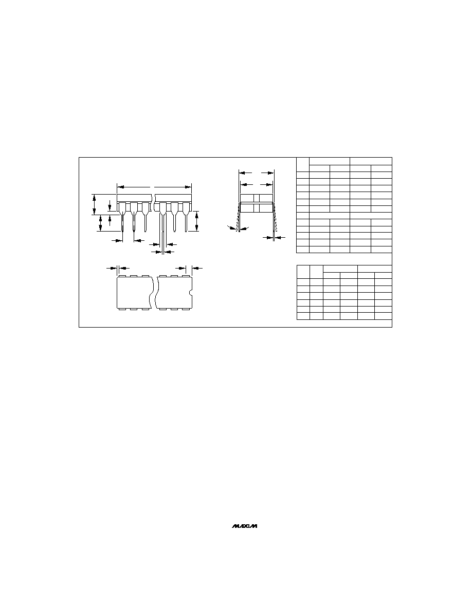
________________________________________________________Package Information
DIM
A
A1
A2
A3
B
B1
C
D1
E
E1
e
eA
eB
L
MIN
≠
0.015
0.125
0.055
0.016
0.045
0.008
0.005
0.300
0.240
0.100
0.300
≠
0.115
MAX
0.200
≠
0.175
0.080
0.022
0.065
0.012
0.080
0.325
0.310
≠
≠
0.400
0.150
MIN
≠
0.38
3.18
1.40
0.41
1.14
0.20
0.13
7.62
6.10
2.54
7.62
≠
2.92
MAX
5.08
≠
4.45
2.03
0.56
1.65
0.30
2.03
8.26
7.87
≠
≠
10.16
3.81
INCHES
MILLIMETERS
Plastic DIP
PLASTIC
DUAL-IN-LINE
PACKAGE
(0.300 in.)
DIM
D
D
D
D
D
D
PKG.
P
P
P
P
P
N
MIN
0.348
0.735
0.745
0.885
1.015
1.14
MAX
0.390
0.765
0.765
0.915
1.045
1.265
MIN
8.84
18.67
18.92
22.48
25.78
28.96
MAX
9.91
19.43
19.43
23.24
26.54
32.13
INCHES
MILLIMETERS
PINS
8
14
16
18
20
24
C
A
A2
E1
D
E
eA
eB
A3
B1
B
0∞ - 15∞
A1
L
D1
e
21-0043A
DIM
A
A1
B
C
E
e
H
L
MIN
0.093
0.004
0.014
0.009
0.291
0.394
0.016
MAX
0.104
0.012
0.019
0.013
0.299
0.419
0.050
MIN
2.35
0.10
0.35
0.23
7.40
10.00
0.40
MAX
2.65
0.30
0.49
0.32
7.60
10.65
1.27
INCHES
MILLIMETERS
21-0042A
Wide SO
SMALL-OUTLINE
PACKAGE
(0.300 in.)
DIM
D
D
D
D
D
MIN
0.398
0.447
0.496
0.598
0.697
MAX
0.413
0.463
0.512
0.614
0.713
MIN
10.10
11.35
12.60
15.20
17.70
MAX
10.50
11.75
13.00
15.60
18.10
INCHES
MILLIMETERS
PINS
16
18
20
24
28
1.27
0.050
L
H
E
D
e
A
A1
C
0∞- 8∞
0.101mm
0.004in.
B
Maxim cannot assume responsibility for use of any circuitry other than circuitry entirely embodied in a Maxim product. No circuit patent licenses are
implied. Maxim reserves the right to change the circuitry and specifications without notice at any time.
12
__________________Maxim Integrated Products, 120 San Gabriel Drive, Sunnyvale, CA 94086 (408) 737-7600
© 1995 Maxim Integrated Products
Printed USA
is a registered trademark of Maxim Integrated Products.
DG528/DG529
8-Channel Latchable Multiplexers
Maxim cannot assume responsibility for use of any circuitry other than circuitry entirely embodied in a Maxim product. No circuit patent licenses are
implied. Maxim reserves the right to change the circuitry and specifications without notice at any time.
12
__________________Maxim Integrated Products, 120 San Gabriel Drive, Sunnyvale, CA 94086 (408) 737-7600
© 1995 Maxim Integrated Products
Printed USA
is a registered trademark of Maxim Integrated Products.
___________________________________________Package Information (continued)
C
0∞-15∞
A
D
B1
B
DIM
A
B
B1
C
E
E1
e
L
L1
Q
S
S1
MIN
≠
0.014
0.038
0.008
0.220
0.290
0.125
0.150
0.015
≠
0.005
MAX
0.200
0.023
0.065
0.015
0.310
0.320
0.200
≠
0.070
0.098
≠
MIN
≠
0.36
0.97
0.20
5.59
7.37
3.18
3.81
0.38
≠
0.13
MAX
5.08
0.58
1.65
0.38
7.87
8.13
5.08
≠
1.78
2.49
≠
2.54
0.100
Q
L
S1
e
CERDIP
CERAMIC DUAL-IN-LINE
PACKAGE
(0.300 in.)
S
L1
E
E1
PINS
8
14
16
18
20
24
DIM
D
D
D
D
D
D
MIN
≠
≠
≠
≠
≠
≠
MAX
0.405
0.785
0.840
0.960
1.060
1.280
MIN
≠
≠
≠
≠
≠
≠
MAX
10.29
19.94
21.34
24.38
26.92
32.51
INCHES
MILLIMETERS
INCHES
MILLIMETERS
21-0045A