
1 of 21
021403
FEATURES
ß User-Programmable Frequency Synthesizer
ß Programmable From 4.1kHz to 66MHz
ß Dual Synchronous Outputs
ß 4.13MHz to 66MHz Reference Oscillator
Output
ß 4.1kHz to 66MHz Main Oscillator Output
ß Single 3.0 to 3.6V Supply
ß Three Resolution Options
ß 2-Wire Serial Interface
ß 0.75% Absolute Accuracy
ß Nonvolatile (NV) Frequency Settings
ß No External Timing Components
ß Power-Down Mode
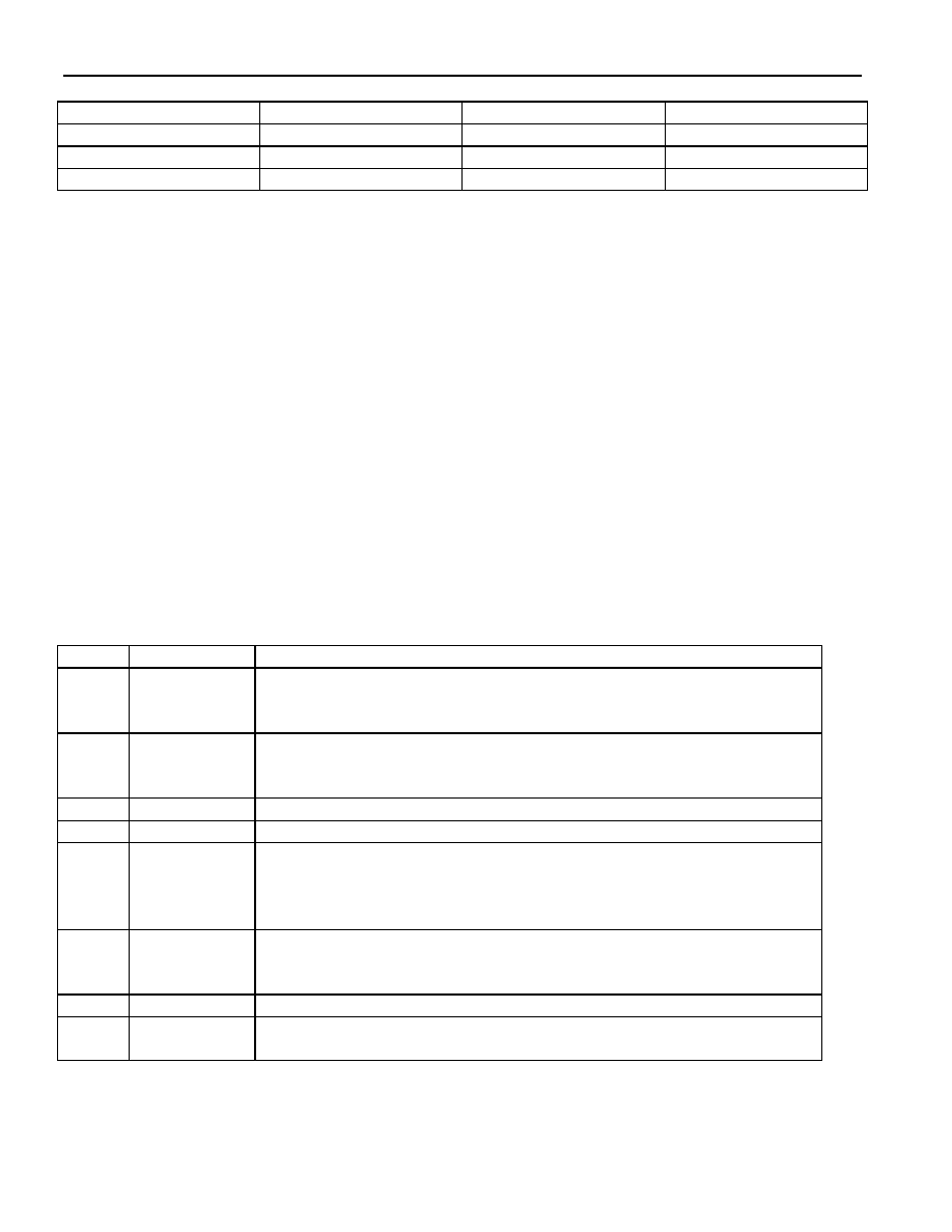
ORDERING INFORMATION
PIN ASSIGNMENT
SO (150mil)
PIN DESCRIPTION
OUT1
- Main Oscillator Output
OUT0
- Reference Oscillator Output
V
CC
- Power-Supply Voltage
GND -
Ground
CTRL1
- Control Pin for OUT1
CTRL0
- Control Pin for OUT0
SDA
- 2-Wire Serial Data Input/Output
SCL
- 2-Wire Serial Clock
DEVICE
PACKAGE
STEP
SIZE
OSCILLATOR
OUTPUT RANGE
DS1085LZ-5
150mil SO
5kHz
4.1kHz to 66MHz
DS1085LZ-12
150mil SO
12.5kHz
4.1kHz to 66MHz
DS1085LZ-25
150mil SO
25kHz
4.1kHz to 66MHz
DESCRIPTION
The DS1085L is a dual-output frequency synthesizer requiring no external timing components for
operation. It can be used as a standalone oscillator or as a dynamically programmed, processor-controlled
peripheral device. An internal master oscillator can be programmed from 33MHz to 66MHz with three
resolution options of 5kHz, 12.5kHz, and 25kHz. A programmable 3-bit prescaler (divide-by-1, 2, 4, or 8)
permits the generation of a reference oscillator output (OUT0) from the master, ranging from 4.13MHz to
66MHz. A second independent prescaler and a 1-to-1025 divider allow the generation of a main oscillator
output (OUT1) from 4.1kHz to 66MHz. The two outputs, although synchronous with the master, can be
independently programmed. The combination of programmable master oscillator, prescalers, and dividers
allows the generation of thousands of user-specified frequencies. All master oscillator, prescaler, and
divider settings are stored in NV (EEPROM) memory, providing a default value on power-up that allows
it to be used as a standalone oscillator. A 2-wire serial interface allows in-circuit, on-the-fly programming
of the master oscillator, prescalers (P0 and P1), and divider (N). This allows dynamic frequency
modification, if required, or, for fixed-frequency applications, the DS1085L can be used with factory- or
user-programmed values.
DS1085L
3.3V EconOscillator Frequency
Synthesizer
www.maxim-ic.com
SCL
CTRL0
SDA
CTRL1
OUT1
OUT0
V
CC
GND
8
7
6
5
1
2
3
4
EconOscillator is a trademark of Dallas Semiconductor.
DS1085L
2 of 21
External control inputs, CTRL1 and CTRL0, enable or disable the two oscillator outputs. Both outputs
feature a synchronous enable that ensures no output glitches when the output is enabled and a constant
time interval (for a given frequency setting) from an enable signal to the first output transition. These
inputs can also be configured to disable the master oscillator, putting the device into a low-power mode
for power-sensitive applications.
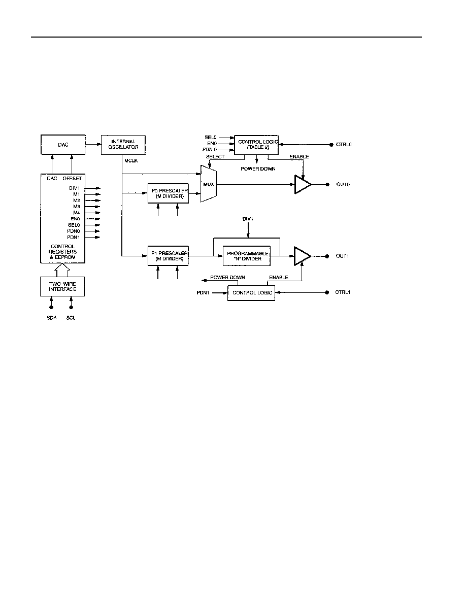
Figure 1. DS1085L BLOCK DIAGRAM
OVERVIEW
A block diagram of the DS1085L is shown in Figure 1. The DS1085L consists of five major components:
ß Internal master oscillator (33MHz to 66MHz)
ß Master oscillator control DAC
ß Prescalers (divide-by-1, 2, 4, or 8)
ß Programmable divider (divide-by-1 to 1025)
ß Control registers
The internal master oscillator provides the reference clock (MCLK), which is fed to the prescalers and
programmable dividers. The frequency of the oscillator can be user-programmed over a two-to-one range
in increments equal to the step size, by means of a 10-bit control DAC. The master oscillator range is
33MHz to 66MHz, which is larger than the range possible with the 10-bit DAC resolution and available
step sizes. Therefore, an additional register (OFFSET) is provided that can be used to select the range of
frequency over which the DAC is used (see Table 1).
0M0
0M1
1M0
1M1
DS1085L
3 of 21
Table 1. DEVICE COMPARISONS BY PART NUMBER
PART NUMBER
STEP SIZE (kHz)
DAC SPAN (MHz)
OFFSET SIZE (MHz)
DS1085LZ-5
5
5.12
2.56
DS1085LZ-12
12.5
12.80
3.20
DS1085LZ-25
25
25.60
3.20
For further description of use of the OFFSET register see the REGISTER FUNCTIONS section.
The master clock can be routed directly to the outputs (OUT0 and OUT1) or through separate prescalers
(P0 and P1). In the case of OUT1, an additional programmable divider (N) can be used to generate
frequencies down to 4.1kHz.
The prescaler (P0) divides MCLK by 1, 2, 4, or 8 before routing MCLK to the reference output (OUT0)
pin.
The prescaler (P1) divides MCLK by 1, 2, 4, or 8 before routing MCLK to the programmable divider (N),
and ultimately to the main output (OUT1) pin.
The programmable divider (N) divides the prescaler output (P1) by any number selected between two and
1025 (10 bits) to provide the main output (OUT1), or it can be bypassed altogether by use of the DIV1
register bit. The value of N is stored in the DIV register.
The control registers are user-programmable through a 2-wire serial interface to determine operating
frequency (values of DAC, OFFSET, P0, P1, and N) and modes of operation. Once programmed, the
register settings are nonvolatile and only need reprogramming if it is desired to reconfigure the device.
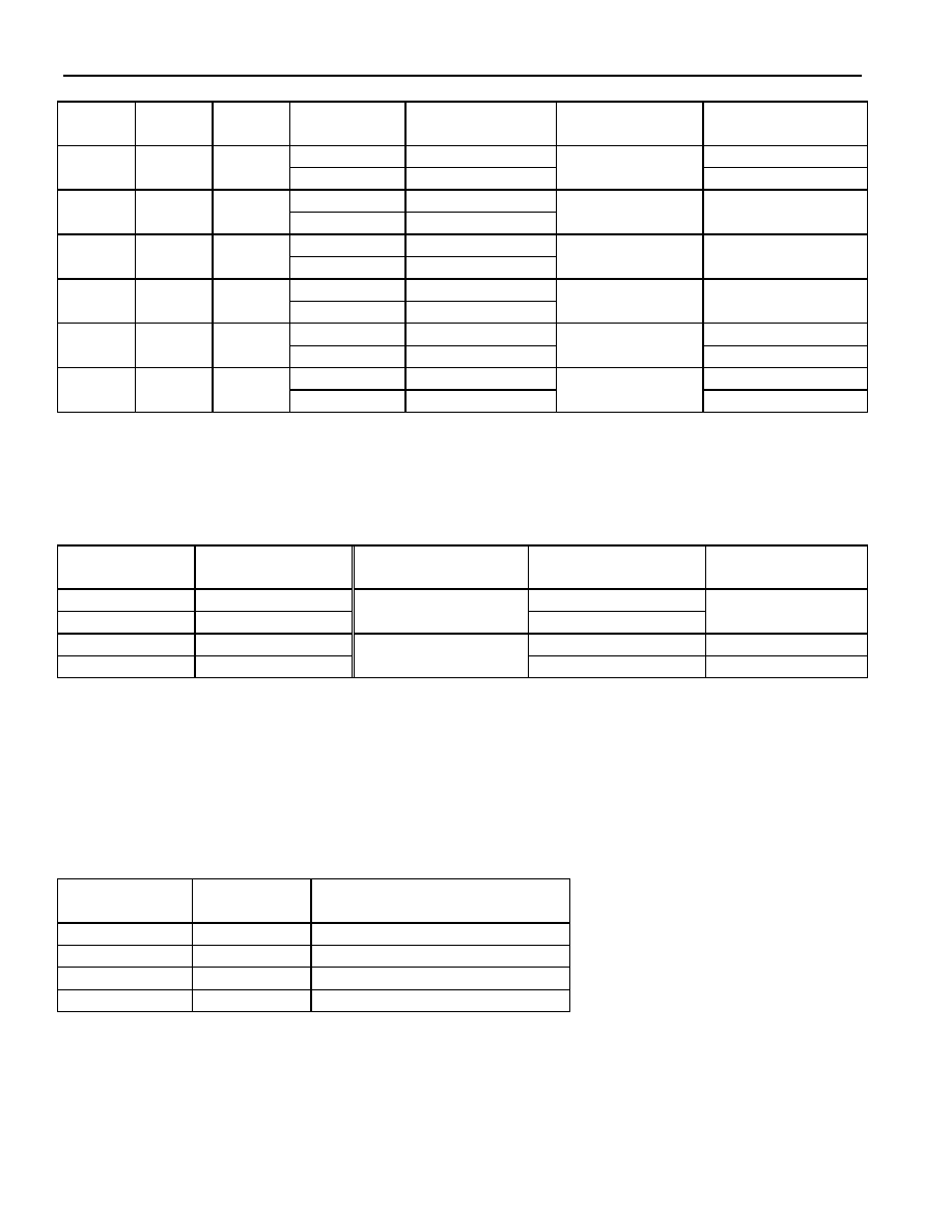
PIN DESCRIPTIONS
PIN
NAME
FUNCTION
1
OUT1
This main oscillator output frequency is determined by the control
register settings for the oscillator (DAC and OFFSET), prescaler P1
(mode bits 1M0 and 1M1), and divider N (DIV).
2
OUT0
The reference output is taken from the output of the reference select mux.
Its frequency is determined by the control register settings for prescaler
P0 (mode bits 0M0 and 0M1) (see Table 2).
3
Vcc
Power Supply
4
GND
Ground
5
CTRL0
A multifunction control input pin that can be programmed to function as
a mux select, ouput enable, and/or a power-down. Its function is
determined by the user-programmable control register values of EN0,
SEL0, and PDN0 (see Table 2).
6
CTRL1
A multifunction control input pin that can be programmed to function as
an output enable and/or a power-down. Its function is determined by the
user-programmable control register value of PDN1 (see Table 3).
7
SDA
I/O pin for the 2-wire serial interface used for data transfer.
8
SCL
Input pin for the 2-wire serial interface used to synchronize data
movement over the serial interface.
DS1085L
4 of 21
Table 2. DEVICE MODE USING OUT0
EN0
(BIT)
SEL0
(BIT)
PDN0
(BIT)
CTRL0
(PIN)
OUT0
(PIN)
CTRL0
FUNCTION
DEVICE
MODE
1
High-Z
Power-Down***
0
0
0
0
High-Z
Power-Down*
Active
1
MCLK/M
0
1
0
0
MCLK
Mux Select
Active
1
High-Z
1
0
0
0
MCLK
Output Enable
Active
1
High-Z
1
1
0
0
MCLK/M
Output Enable
Active**
1
High-Z
Power-Down
X
0
1
0
MCLK
Power-Down
Active
1
High-Z
Power-Down
X
1
1
0
MCLK/M
Power-Down
Active
* This mode is for applications where OUT0 is not used, but CTRL0 is used as a device shutdown.
** Factory default setting.
***See standby (power-down) current specification for power-down current range.
Table 3. DEVICE MODE USING OUT1
PDN1
(BIT)
CTRL1
(PIN)
CTRL1
FUNCTION
OUT1 (PIN)
DEVICE MODE
0
0
OUT CLK
0
1
Output Enable
High-Z
Active*
1
0
OUT CLK
Active
1
1
Power-Down
High-Z
Power-Down
*Factory default setting
NOTE:
Both CTRL0 and CTRL1 can be configured as power-downs. They are internally "OR" connected so
either of the control pins can be used to provide a power-down function for the whole device, subject to
appropriate settings of the PDN0 and PDN1 register bits (see Table 4).
Table 4. SHUTDOWN CONTROL WITH PDN0 AND PDN1
PDN0
(BIT)
PDN1
(BIT)
SHUTDOWN CONTROL
0
0
NONE
0
1
CTRL1
1
0
CTRL0
1
1
CTRL1 OR CTRL0
DS1085L
5 of 21
REGISTER FUNCTIONS
The user-programmable registers can be used to determine the mode of operation (MUX), operating
frequency (DAC, OFFSET, DIV), and bus settings (ADDR). The functions of the registers are described
in this section, but the details of how these registers are programmed can be found in a later section. The
register settings are nonvolatile, with the values being stored automatically or as required in EEPROM
when the registers are programmed through the SDA and SCL pins.
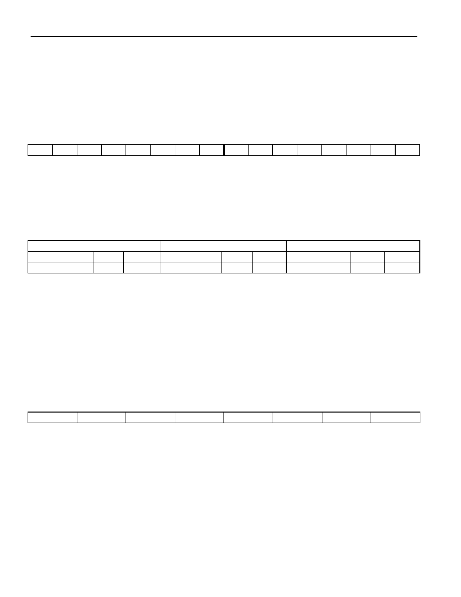
DAC WORD
(Address 08h)
MSB
LSB MSB
LSB
d9
d8
d7
d6
d5
d4
d3
d2
d1
d0
X
X
X
X
X
X
First Data Byte
Second Data Byte
X = Don't care.
The DAC word (d0≠d9) controls the frequency of the master oscillator. The resolution of this register
depends on the step size of the device. The absolute frequency of the device also depends on the value of
the OFFSET register (see Tables 5 and 6).
Table 5. DEVICE DEFAULT SETTINGS
DS1085LZ-5
DS1085LZ-12
DS1085LZ-25
Frequency
DAC
Offset
Frequency
DAC
Offset
Frequency
DAC
Offset
48.58MHz
500
OS
52.3MHz
600
OS
50.9MHz
500
OS
For any given value of OFFSET the master oscillator frequency can be derived as follows:
Frequency = Min Frequency + DAC x Step Size
where: Min frequency is the lowest frequency shown in Table 6 for the corresponding offset.
DAC is the value of the DAC register (0≠1023).
Step size is the step size of the device (5kHz, 12.5kHz, or 25kHz).
OS is the decimal, integer value of the 5 MSBs of the RANGE register.
OFFSET BYTE
(Address 0Eh)
MSB
LSB
X
X
X
O4
O3
O2
O1
O0
X = Don't care.
The OFFSET byte (O0≠O4) determines the range of frequencies that can be obtained within the absolute
minimum and maximum range of the oscillator. Correct operation of the device is not guaranteed for
values of OFFSET not shown in Table 6.