 | –≠–ª–µ–∫—Ç—Ä–æ–Ω–Ω—ã–π –∫–æ–º–ø–æ–Ω–µ–Ω—Ç: DS1086L | –°–∫–∞—á–∞—Ç—å:  PDF PDF  ZIP ZIP |

General Description
The DS1086L EconOscillatorTM is a 3.3V programmable
clock generator that produces a spread-spectrum
(dithered) square-wave output of frequencies from
130kHz to 66.6MHz. The selectable dithered output
reduces radiated-emission peaks by dithering the fre-
quency 0.5%,1%, 2%, 4%, or 8% below the pro-
grammed frequency. The DS1086L has a power-down
mode and an output-enable control for power-sensitive
applications. All the device settings are stored in non-
volatile (NV) EEPROM memory allowing it to operate in
stand-alone applications.
Applications
Printers
Copiers
PCs
Computer Peripherals
Cell Phones
Cable Modems
Features
User-Programmable Square-Wave Generator
Frequencies Programmable from 130kHz to
66.6MHz
0.5%, 1%, 2%, 4%, or 8% Selectable Dithered
Output
Adjustable Dither Rate
Glitchless Output-Enable Control
2-Wire Serial Interface
Nonvolatile Settings
2.7V to 3.6V Supply
No External Timing Components Required
Power-Down Mode
5kHz Master Frequency Step Size
EMI Reduction
Industrial Temperature Range: -40∞C to +85∞C
DS1086L
3.3V Spread-Spectrum EconOscillator
______________________________________________ Maxim Integrated Products
1
PDN
OE
GND
1
2
8
7
SCL
SDA
SPRD
V
CC
OUT
µSOP
TOP VIEW
3
4
6
5
DS1086L
Pin Configuration
Ordering Information
DS1086L
XTL1/OSC1
µP
XTL2/OSC2
DITHERED 130kHz TO
66.6MHz OUTPUT
DECOUPLING CAPACITORS
(0.1
µF and 0.01µF)
*SDA AND SCL CAN BE CONNECTED DIRECTLY HIGH IF THE DS1086L NEVER NEEDS
TO BE PROGRAMMED IN-CIRCUIT, INCLUDING DURING PRODUCTION TESTING.
SPRD
OUT
V
CC
V
CC
V
CC
GND
N.C.
SCL*
SDA*
PDN
OE
Typical Operating Circuit
Rev 0; 11/03
For pricing, delivery, and ordering information, please contact Maxim/Dallas Direct! at
1-888-629-4642, or visit Maxim's website at www.maxim-ic.com.
PART
TEMP RANGE
PIN-PACKAGE
DS1086LU
-40∞C to +85∞C
8
µSOP (118 mil)
EconOscillator is a trademark of Dallas Semiconductor.

DS1086L
3.3V Spread-Spectrum EconOscillator
2
_____________________________________________________________________
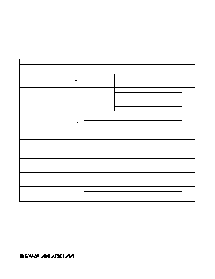
ABSOLUTE MAXIMUM RATINGS
RECOMMENDED DC OPERATING CONDITIONS
(V
CC
= 2.7V to 3.6V, T
A
= -40∞C to +85∞C.)
Stresses beyond those listed under "Absolute Maximum Ratings" may cause permanent damage to the device. These are stress ratings only, and functional
operation of the device at these or any other conditions beyond those indicated in the operational sections of the specifications is not implied. Exposure to
absolute maximum rating conditions for extended periods may affect device reliability.
PARAMETER
SYMBOL
CONDITIONS
MIN
TYP
MAX
UNITS
Supply Voltage
V
CC
(Note 1)
2.7
3.3
3.6
V
High-Level Input Voltage
(SDA, SCL, SPRD,
PDN, OE)
V
IH
0.7 x
V
CC
V
CC
+
0.3
V
Low-Level Input Voltage
(SDA, SCL SPRD,
PDN, OE)
V
IL
-0.3
0.3 x
V
CC
V
DC ELECTRICAL CHARACTERISTICS
(V
CC
= 2.7V to 3.6V, T
A
= -40∞C to +85∞C.)
PARAMETER
SYMBOL
CONDITIONS
MIN
TYP
MAX
UNITS
High-Level Output Voltage (OUT)
V
OH
I
OH
= -4mA, V
CC
= min
2.4
V
Low-Level Output Voltage (OUT)
V
OL
I
OL
= 4mA
0
0.4
V
V
OL1
3mA sink current
0
0.4
Low-Level Output Voltage (SDA)
V
OL2
6mA sink current
0
0.6
V
High-Level Input Current
I
IH
V
CC
= 3.6V
1
µA
Low-Level Input Current
I
IL
V
IL
= 0
-1
µA
Supply Current (Active)
I
CC
C
L
= 15pF (output at default frequency)
10
mA
Standby Current (Power-Down)
I
CCQ
Power-down mode
10
µA
Voltage Range on V
CC
Relative to Ground ..........-0.5V to +6.0V
Voltage Range on SPRD,
PDN, OE, SDA, and SCL
Relative to Ground* ..................................-0.5 to (V
CC
+ 0.5V)
Operating Temperature Range ...........................-40∞C to +85∞C
Programming Temperature Range .........................0∞C to +70∞C
Storage Temperature Range .............................-55∞C to +125∞C
Soldering Temperature ..................See IPC/JEDEC J-STD-020A
*This voltage must not exceed 6.0V.
DS1086L
3.3V Spread-Spectrum EconOscillator
_____________________________________________________________________
3
MASTER OSCILLATOR CHARACTERISTICS
(V
CC
= 2.7V to 3.6V, T
A
= -40∞C to +85∞C.)
PARAMETER
SYMBOL
CONDITIONS
MIN
TYP
MAX
UNITS
Master Oscillator Frequency
f
OSC
(Note 2)
33.3
66.6
MHz
Default Master Oscillator Frequency
f
0
Factory-programmed default
48.65
MHz
Default frequency (f
0
)
-0.5
+0.5
Master Oscillator Frequency
Tolerance
f
0
f
0
V
CC
= 3.3V,
T
A
= +25
∞C
(Notes 3,17)
DAC step size
-0.5
+0.5
%
Default frequency
-0.75
+0.75
Voltage Frequency Variation
f
V
f
0
Over voltage range,
T
A
= +25
∞C (Note 4) DAC step size
-0.75
+0.75
%
Default frequency
-2.0
+0.75
66.6MHz
-2.0
+0.75
Temperature Frequency Variation
f
T
f
0
Over temperature
range, V
CC
= 3.3V
(Note 5)
33.3MHz
-2.5
+0.75
%
Prescaler bits JS2, JS1, JS0 = 000
0.5
Prescaler bits JS2, JS1, JS0 = 001
1
Prescaler bits JS2, JS1, JS0 = 010
2
Prescaler bits JS2, JS1, JS0 = 100
4
Dither Frequency Range (Note 6)
f
f
0
Prescaler bits JS2, JS1, JS0 = 111
8
%
Integral Nonlinearity of Frequency
INL
Entire range (Note 7)
-0.6
+0.3
%
DAC Step Size
between two consecutive DAC values
(Note 8)
5
kHz
DAC Span
Frequency range for one offset setting
(Table 2)
5.12
MHz
DAC Default
Factory default register setting
500
decimal
Offset Step Size
between two consecutive offset values
(Table 2)
2.56
MHz
Offset Default
OS
Factory default OFFSET register setting
(5 LSBs) (Table 2)
RANGE
(5 LSBs of
RANGE register)
hex
Prescaler bits JS4, JS3 = 00
f
0
/8192
Prescaler bits JS4, JS3 = 01
f
0
/4096
Dither Rate
Prescaler bits JS4, JS3 = 10
f
0
/2048
Hz

DS1086L
3.3V Spread-Spectrum EconOscillator
4
_____________________________________________________________________
AC ELECTRICAL CHARACTERISTICS
(V
CC
= 2.7V to 3.6V, T
A
= -40∞C to +85∞C.)
PARAMETER
SYMBOL
CONDITIONS
MIN
TYP
MAX
UNITS
Frequency Stable After Prescaler
Change
1
period
Frequency Stable After DAC or
Offset Change
t
DACstab
(Note 9)
0.1
1
ms
Power-Up Time
t
por
+ t
stab
(Note 10)
0.1
0.5
ms
Enable of OUT After Exiting
Power-Down Mode
t
stab
(Note 18)
200
µs
OUT High-Z After Entering
Power-Down Mode
t
pdn
100
µs
Load Capacitance
C
L
(Note 11)
15
50
pF
Output Duty Cycle (OUT)
Default frequency
45
55
%
Rise and Fall Time (OE,
PDN)
1
µs
AC ELECTRICAL CHARACTERISTICS--2-WIRE INTERFACE
(V
CC
= 2.7V to 3.6V, T
A
= -40∞C to +85∞C.)
PARAMETER
SYMBOL
CONDITIONS
MIN
TYP
MAX
UNITS
Fast mode
400
SCL Clock Frequency
f
SCL
Standard mode
(Note 12)
100
kHz
Fast mode
1.3
Bus Free Time Between a STOP
and START Condition
t
BUF
Standard mode
(Note 12)
4.7
µs
Fast mode
0.6
Hold Time (Repeated) START
Condition
t
HD:STA
Standard mode
(Notes 12, 13)
4.0
µs
Fast mode
1.3
LOW Period of SCL
t
LOW
Standard mode
(Note 12)
4.7
µs
Fast mode
0.6
HIGH Period of SCL
t
HIGH
Standard mode
(Note 12)
4.0
µs
Fast mode
0.6
Setup Time for a Repeated
START
t
SU:STA
Standard mode
(Note 12)
4.7
µs
Fast mode
Data Hold Time
t
HD:DAT
Standard mode
(Notes 12, 14, 15)
0
0.9
µs
Fast mode
100
Data Setup Time
t
SU:DAT
Standard mode
(Note 12)
250
ns
Fast mode
20 + 0.1C
B
300
Rise Time of Both SDA and SCL
Signals
t
R
Standard mode
(Note 16)
20 + 0.1C
B
1000
ns
Fast mode
20 + 0.1C
B
300
Fall Time of Both SDA and SCL
Signals
t
F
Standard mode
(Note 16)
20 + 0.1C
B
1000
ns

DS1086L
3.3V Spread-Spectrum EconOscillator
_____________________________________________________________________
5
AC ELECTRICAL CHARACTERISTICS--2-WIRE INTERFACE (continued)
(V
CC
= 2.7V to 3.6V, T
A
= -40∞C to +85∞C.)
PARAMETER
SYMBOL
CONDITIONS
MIN
TYP
MAX
UNITS
Fast mode
0.6
Setup Time for STOP
t
SU:STO
Standard mode
4.0
µs
Capacitive Load for Each Bus
Line
C
B
(Note 16)
400
pF
EEPROM Write Cycle Time
t
WR
10
ms
Input Capacitance
C
I
5
pF
NONVOLATILE MEMORY CHARACTERISTICS
(V
CC
= 2.7V to 3.6V)
PARAMETER
SYMBOL
CONDITIONS
MIN
TYP
MAX
UNITS
EEPROM Writes
+70∞C
10,000
Note 1:
All voltages are referenced to ground.
Note 2:
DAC and OFFSET register settings must be configured to maintain the master oscillator frequency within this range.
Correct operation of the device is not guaranteed if these limits are exceeded.
Note 3:
This is the absolute accuracy of the master oscillator frequency at the default settings.
Note 4:
This is the change that is observed in master oscillator frequency with changes in voltage from nominal voltage at
T
A
= +25∞C.
Note 5:
This is the percentage frequency change from the +25∞C frequency due to temperature at V
CC
= 3.3V. The maximum temper-
ature change varies with the master oscillator frequency setting. The minimum occurs at the default master oscillator frequen-
cy (f
default
). The maximum occurs at the extremes of the master oscillator frequency range (33.3MHz or 66.6MHz).
Note 6:
The dither deviation of the master oscillator frequency is unidirectional and lower than the undithered frequency.
Note 7:
The integral nonlinearity of the frequency is a measure of the deviation from a straight line drawn between the two end-
points (f
osc(MIN)
to f
osc(MAX)
) of the range. The error is in percentage of the span.
Note 8:
This is true when the prescaler = 1.
Note 9:
Frequency settles faster for small changes in value. During a change, the frequency transitions smoothly from the original
value to the new value.
Note 10:
This indicates the time elapsed between power-up and the output becoming active. An on-chip delay is intentionally
introduced to allow the oscillator to stabilize. t
stab
is equivalent to approximately 512 master clock cycles and therefore
depends on the programmed clock frequency.
Note 11:
Output voltage swings can be impaired at high frequencies combined with high output loading.
Note 12:
A fast-mode device can be used in a standard-mode system, but the requirement t
SU:DAT
> 250ns must then be met.
This is automatically the case if the device does not stretch the LOW period of the SCL signal. If such a device does
stretch the LOW period of the SCL signal, it must output the next data bit to the SDA line at least t
R MAX
+ t
SU:DAT
=
1000ns + 250ns = 1250ns before the SCL line is released.
Note 13:
After this period, the first clock pulse is generated.
Note 14:
A device must internally provide a hold time of at least 300ns for the SDA signal (referred to as the V
IH MIN
of the SCL
signal) to bridge the undefined region of the falling edge of SCL.
Note 15:
The maximum t
HD:DAT
need only be met if the device does not stretch the LOW period (t
LOW
) of the SCL signal.
Note 16:
C
B
--total capacitance of one bus line, timing referenced to 0.9 x V
CC
and 0.1 x V
CC
.
Note 17:
Typical frequency shift due to aging is ±0.5%. Aging stressing includes Level 1 moisture reflow preconditioning (24hr
+125∞C bake, 168hr 85∞C/85%RH moisture soak, and three solder reflow passes +240 +0/-5∞C peak) followed by 1000hr
max V
CC
biased 125∞C HTOL, 1000 temperature cycles at -55∞C to +125∞C, 96hr 130∞C/85%RH/3.6V HAST and 168hr
121∞C/2 ATM Steam/Unbiased Autoclave.
Note 18:
t
stab
is the time required after exiting power-down to the beginning of output oscillations. In addition, a delay of t
DACstab
is required before the frequency will be within its specified tolerance.