 | ÐлекÑÑоннÑй компоненÑ: DS1090U-4 | СкаÑаÑÑ:  PDF PDF  ZIP ZIP |
Äîêóìåíòàöèÿ è îïèñàíèÿ www.docs.chipfind.ru

General Description
The DS1090 is a low-cost, dithered oscillator intended
to be used as an external clock for switched-mode
power supplies and other low-frequency applications.
The dithering or sweeping function reduces peak-radi-
ated emissions from the power supply at its fundamen-
tal frequency, as well as harmonic frequencies. The
device consists of a resistor-programmed master oscil-
lator, factory-programmed clock prescaler, and a pin-
programmed dither circuit. These features allow the
DS1090 to be used in applications where a spread-
spectrum clock is desired to reduce radiated emis-
sions. A combination of factory-set prescalers and
external resistor allows for output frequencies ranging
from 125kHz to 8MHz. Both dither frequency and dither
percentage are set using control pins.
Applications
Switched-Mode Power Supplies
Servers
Printers
Embedded Microcontrollers
Industrial Controls
Automotive Applications
Features
Low-Cost, Spread-Spectrum EconOscillatorTM
Simple User Programming
Output Frequency Programmable from 125kHz
to 8MHz
Dither Percentage Programmable from 0% to 8%
Dither Rate Programmable (f
MOSC
/ 512, 1024,
2048, or 4096 )
3.0V to 5.5V Single-Supply Operation
CMOS/TTL-Compatible Output
Operating Temperature Range: -40°C to +85°C
DS1090
Low-Frequency, Spread-Spectrum
EconOscillator
______________________________________________ Maxim Integrated Products
1
J1
J0
GND
1
2
8
7
JC1
JC0
R
SET
V
CC
OUT
µSOP
TOP VIEW
3
4
6
5
DS1090
Pin Configuration
Ordering Information
DS1090
V
OUT
V
IN
DC-DC
STEP-DOWN
CONVERTER
OUT
GND
V
CC
V
CC
R
SET
JC0
JC1
J0
J1
45k
TO 91k
Typical Operating Circuit
Rev 0; 4/04
For pricing, delivery, and ordering information, please contact Maxim/Dallas Direct! at
1-888-629-4642, or visit Maxim's website at www.maxim-ic.com.
Add "/T" for Tape & Reel orders.
*Contact factory for availability.
PART
OUTPUT
FREQUENCY
RANGE
PRESCALER
PIN-
PACKAGE
DS1090U-1
4MHz to 8MHz
1
8 µSOP
DS1090U-2*
2MHz to 4MHz
2
8 µSOP
DS1090U-4*
1MHz to 2MHz
4
8 µSOP
DS1090U-8*
500kHz to 1MHz
8
8 µSOP
DS1090U-16
250kHz to
500kHz
16
8 µSOP
DS1090U-32*
125kHz to
250kHz
32
8 µSOP
EconOscillator is a trademark of Dallas Semiconductor.

DS1090
Low-Frequency, Spread-Spectrum
EconOscillator
2
_____________________________________________________________________
ABSOLUTE MAXIMUM RATINGS
RECOMMENDED DC OPERATING CONDITIONS
(T
A
= -40°C to +85°C)
DC ELECTRICAL CHARACTERISTICS
(V
CC
= +3.0V to +5.5V, T
A
= -40°C to +85°C, unless otherwise noted.)
Stresses beyond those listed under "Absolute Maximum Ratings" may cause permanent damage to the device. These are stress ratings only, and functional
operation of the device at these or any other conditions beyond those indicated in the operational sections of the specifications is not implied. Exposure to
absolute maximum rating conditions for extended periods may affect device reliability.
Voltage Range on V
CC
Relative to Ground ...........-0.5V to +6.0V
Voltage Range on Input Pins
Relative to Ground.................................-0.5V to (V
CC
+ 0.5V),
not to exceed 6.0V
Operating Temperature Range ...........................-40
°C to +85°C
Storage Temperature Range .............................-55
°C to +125°C
Soldering Temperature .......................................See IPC/JEDEC
J-STD-020A Specification
PARAMETER
SYMBOL
CONDITIONS
MIN
TYP
MAX
UNITS
Supply Voltage
V
CC
(Note 1)
3.0
5.5
V
Input Logic 1 (J0, J1, JC0, JC1)
V
IH
0.7 x
V
CC
V
CC
+
0.3
V
Input Logic 0 (J0, J1, JC0, JC1)
V
IL
-0.3
+0.3 x
V
CC
V
PARAMETER
SYMBOL
CONDITIONS
MIN
TYP
MAX
UNITS
C
L
= 15pF, V
CC
= 3.3V, R
SET
= 40k
1.4
Supply Current
I
CC
C
L
= 15pF, V
CC
= 5.5V, R
SET
= 40k
1.7
3
mA
I
OH
= -4mA
High-Level Output Voltage (OUT)
V
OH
V
CC
= min
2.4
V
Low-Level Output Voltage (OUT)
V
OL
I
OL
= 4mA
0.4
V
High-Level Input Current
(J0, J1, JC0, JC1)
I
IH
V
IH
= V
CC
+1.0
µA
Low-Level Input Current
(J0, J1, JC0, JC1)
I
IL
V
IL
= 0V
-1.0
µA
Resistor Current
I
RES
V
CC
= max
150
µA

DS1090
Low-Frequency, Spread-Spectrum
EconOscillator
_____________________________________________________________________
3
PARAMETER
SYMBOL
CONDITIONS
MIN
TYP
MAX
UNITS
Internal Master Oscillator
Frequency
f
MOSC
4.0
8.0
MHz
Output Frequency Tolerance
f
OUT
V
CC
= 3.3V,
T
A
= +25°C
-11.5
+11.5
%
T
A
= +25°C, R
SET
= 60k
,
V
CC
= 3.0V to 3.6V (Notes 2, 3)
-0.3
+0.3
Voltage Frequency Variation
f
OUT
T
A
= +25°C, R
SET
= 60k
,
V
CC
= 4.5V to 5.5V (Notes 2, 3)
-1.25
+1.25
%
Temperature Frequency Variation
f
OUT
V
CC
= 3.3V
(Notes 2, 3, 4)
-2.5
+2.5
%
J0 = GND, J1 = GND
0
J0 = V
CC
, J1 = GND
2
J0 = GND, J1 = V
CC
4
Peak-to-Peak Dither (3
)
(Note 5)
J0 = V
CC
, J1 = V
CC
8
%
Power-Up Time
t
POR
+
t
STAB
(Note 6)
0.1
0.5
ms
Load Capacitance
C
L
(Note 7)
30
pF
4MHz to 8MHz, T
A
= +25°C (Note 3)
45
55
Output Duty Cycle
<4MHz (Note 4)
50
%
Output Rise/Fall Time
t
R
, t
F
C
L
= 15pF
20
ns
AC ELECTRICAL CHARACTERISTICS
(V
CC
= +3.0V to +5.5V, T
A
= -40°C to +85°C, unless otherwise noted.)
Note 1:
All voltages referenced to ground.
Note 2:
This is the change observed in output frequency due to changes in temperature or voltage.
Note 3:
See the Typical Operating Characteristics section.
Note 4:
Parameter is guaranteed by design and is not production tested.
Note 5:
This is a percentage of the output period. Parameter is characterized but not production tested. This can be varied from
0% to 8%.
Note 6:
This indicates the time between power-up and the outputs becoming active. An on-chip delay is intentionally introduced to
allow the oscillator to stabilize. t
STAB
is equivalent to ~500 clock cycles and is dependent upon the programmed
output frequency.
Note 7:
Output voltage swings can be impaired at high frequencies combined with high output loading.
DS1090
Low-Frequency, Spread-Spectrum
EconOscillator
4
_____________________________________________________________________
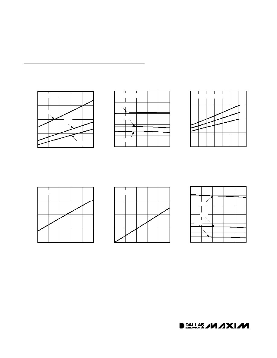
Typical Operating Characteristics
(V
CC
= +3.3V, T
A
= +25°C, unless otherwise noted.)
SUPPLY CURRENT
vs. SUPPLY VOLTAGE
DS1090 toc01
SUPPLY VOLTAGE (V)
SUPPLY CURRENT (mA)
5.0
4.5
4.0
3.5
0.95
1.20
1.45
1.70
0.70
3.0
5.5
NO LOAD, T
A
= +25
°C
40k
60k
80k
SUPPLY CURRENT
vs. TEMPERATURE
DS1090 toc02
TEMPERATURE (
°C)
SUPPLY CURRENT (mA)
60
35
10
-15
0.70
0.90
1.10
1.30
1.50
0.50
-40
85
NO LOAD, V
CC
= 3.3V
40k
60k
80k
SUPPLY CURRENT
vs. OUTPUT LOADING
DS1090 toc03
LOAD CAPACITANCE (pF)
SUPPLY CURRENT (mA)
35
30
25
20
15
10
1
2
3
4
0
5
40
T
A
= +25
°C, R
SET
= 40k
4V
3V
5V
OUTPUT VOLTAGE HIGH
vs. OUTPUT CURRENT
DS1090 toc04
OUTPUT CURRENT (mA)
OUTPUT VOLTAGE (V)
-1
-2
-3
-4
2.8
2.9
3.0
3.1
2.7
-5
0
V
CC
= 3.0V
OUTPUT VOLTAGE LOW
vs. OUTPUT CURRENT
DS1090 toc05
OUTPUT CURRENT (mA)
OUTPUT VOLTAGE (V)
4
3
2
1
0.1
0.2
0.3
0.4
0
0
5
V
CC
= 3.0V
OUTPUT FREQUENCY
vs. SUPPLY VOLTAGE
DS1090 toc06
SUPPLY VOLTAGE (V)
FREQUENCY (MHz)
5.0
4.5
4.0
3.5
5
6
7
8
9
10
4
3.0
5.5
T
A
= +25
°C
60k
80k
40k

DS1090
Low-Frequency, Spread-Spectrum
EconOscillator
_____________________________________________________________________
5
OUTPUT FREQUENCY
vs. TEMPERATURE
DS1090 toc07
TEMPERATURE (
°C)
FREQUENCY (MHz)
60
35
10
-15
5
6
7
8
9
10
4
-40
85
V
CC
= 3.3V
60k
80k
40k
DUTY CYCLE
vs. TEMPERATURE
DS1090 toc08
TEMPERATURE (
°C)
DUTY CYCLE (%)
60
35
10
-15
49
50
51
52
48
-40
85
R
SET
= 40k
V
CC
= 3.3V
V
CC
= 5V
DS1090U-1
RESISTOR CURRENT
vs. RESISTOR VALUE
DS1090 toc09
R
SET
(k
)
RESISTOR CURRENT (
µ
A)
70
60
50
10
12
14
16
18
8
40
80
V
CC
= 3.3V, T
A
= +25
°C
FREQUENCY ERROR
vs. SUPPLY VOLTAGE (FROM 3.3V)
DS1090 toc10
SUPPLY VOLTAGE (V)
FREQUENCY ERROR (%)
5.0
4.5
4.0
3.5
-2.5
0
2.5
5.0
-5.0
3.0
5.5
T
A
= +25
°C
40k
60k
80k
FREQUENCY ERROR
vs. TEMPERATURE (FROM +25
°C)
DS1090 toc11
TEMPERATURE (
°C)
FREQUENCY ERROR (%)
60
35
10
-15
-1.0
0
1.0
2.0
-2.0
-40
85
V
CC
= 3.3V
40k
60k
80k
POWER SPECTRUM vs. SPREAD
DS1090 toc12
FREQUENCY (MHz)
POWER (dBm)
5.35
-70
-60
-50
-40
-30
-20
-10
0
-80
4.80
5.90
V
CC
= 3.3V,
T
A
= +25
°C,
JC0 = JC1 = 1
OFF
±2%
±4%
±8%
Typical Operating Characteristics (continued)
(V
CC
= +3.3V, T
A
= +25°C, unless otherwise noted.)