 | –≠–ª–µ–∫—Ç—Ä–æ–Ω–Ω—ã–π –∫–æ–º–ø–æ–Ω–µ–Ω—Ç: DS1091L | –°–∫–∞—á–∞—Ç—å:  PDF PDF  ZIP ZIP |
General Description
The DS1091L is a low-cost clock generator that is factory-
trimmed to output frequencies from 130kHz to 66.6MHz
with a nominal accuracy of ±0.25%. The device can also
produce a center- or down-dithered spread-spectrum
output with pin-selectable dither magnitude and rate.
Assembled in an 8-pin µMAX package, the DS1091L is
designed to operate with a 3.0V to 3.6V power supply
over the automotive temperature range (-40∞C to
+125∞C).
Applications
Automotive Infotainment
POS Terminals
LCD Displays
Printers
Industrial Control
Features
Spread-Spectrum Clock Output from 130kHz to
66.6MHz
Operating Temperature Range of -40∞C to +125∞C
Accuracy of ±1.75% Across Temperature and
Voltage
Factory Trimmed
Center-Dithered (DS1091LA) or Down-Dithered
(DS1091LB) Spread-Spectrum Output
Pin-Selectable Center-Dither Magnitude of 0%,
±1%, ±2%, or ±4%
Pin-Selectable Down-Dither Magnitude of 0%, -2%,
-4%, or -8%
Pin-Selectable Dither Rate
3.0V to 3.6V Supply Operation
Lead-Free 8-Pin µMAX Package
DS1091L
Automotive Temperature Range
Spread-Spectrum Econoscillator
______________________________________________
Maxim Integrated Products
1
1
2
3
4
8
7
6
5
DR
N.C.
N.C.
SEL0
SEL1
GND
V
CC
OUT
MAX
TOP VIEW
DS1091L
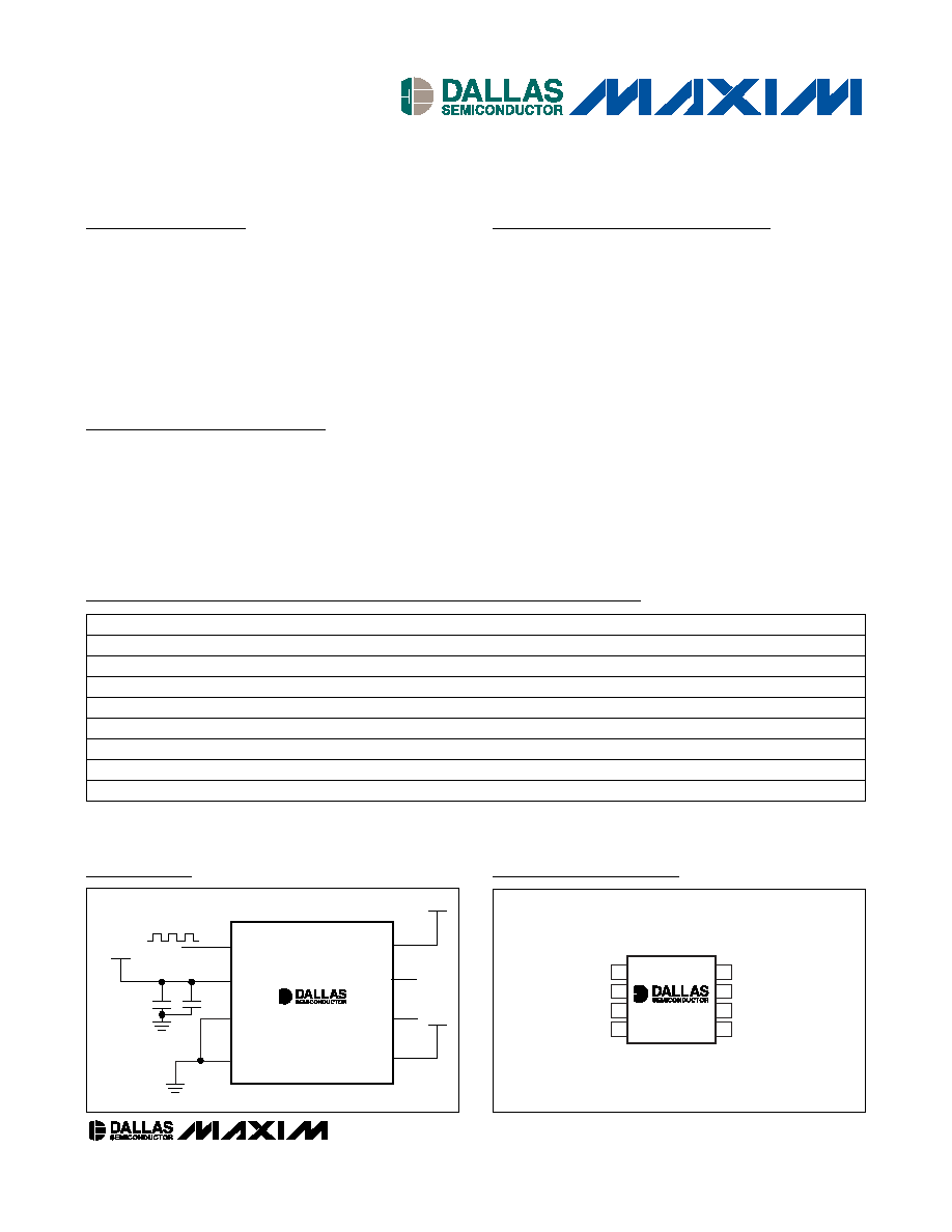
Pin Configuration
8
3
4
2
1
OUT
DR
8 MAX
DS1091L
V
CC
V
CC
f
OUT
DECOUPLING
CAPACITORS
7
6
5
SEL0
V
CC
N.C.
N.C.
SEL1
GND
V
CC
Typical Operating Circuit
Rev 0; 9/06
For pricing, delivery, and ordering information, please contact Maxim/Dallas Direct! at
1-888-629-4642, or visit Maxim's website at www.maxim-ic.com.
+
Denotes lead-free package.
xxx
Denotes factory-programmed custom frequencies.
Email Custom_EconOscillators_Info@dalsemi.com for information/questions concerning custom frequencies.
Ordering Information
PART
TEMP RANGE
PIN-PACKAGE
SPREAD SPECTRUM
OUTPUT FREQUENCY (MHz)
DS1091LUA+027
-40∞C to +125∞C
8 µMAX
Center
27.0
DS1091LUA+033
-40∞C to +125∞C
8 µMAX
Center
33.3
DS1091LUA+066
-40∞C to +125∞C
8 µMAX
Center
66.6
DS1091LUA+xxx
-40∞C to +125∞C
8 µMAX
Center
Custom (Contact Factory)
DS1091LUB+027
-40∞C to +125∞C
8 µMAX
Down
27.0
DS1091LUB+033
-40∞C to +125∞C
8 µMAX
Down
33.3
DS1091LUB+066
-40∞C to +125∞C
8 µMAX
Down
66.6
DS1091LUB+xxx
-40∞C to +125∞C
8 µMAX
Down
Custom (Contact Factory)
µMAX
8 µMAX

ABSOLUTE MAXIMUM RATINGS
RECOMMENDED OPERATING CONDITIONS
(TA = -40∞C to +125∞C.)
Stresses beyond those listed under "Absolute Maximum Ratings" may cause permanent damage to the device. These are stress ratings only, and functional
operation of the device at these or any other conditions beyond those indicated in the operational sections of the specifications is not implied. Exposure to
absolute maximum rating conditions for extended periods may affect device reliability.
Voltage on V
CC
Relative to Ground.......................-0.5V to +6.0V
Voltage on DR, SEL0, SEL1 Relative
to Ground* ..............................................-0.5V to (V
CC
+ 0.5V)
Operating Temperature Range .........................-40∞C to +125∞C
Storage Temperature Range .............................-55∞C to +125∞C
Soldering Temperature...................See J-STD-020 Specification
PARAMETER
SYMBOL
CONDITIONS
MIN
TYP
MAX
UNITS
Supply Voltage
V
CC
(Note 1)
3.0
3.3
3.6
V
High-Level Input Voltage
(SEL0, SEL1, DR)
V
IH
0.7 x
V
CC
V
CC
+
0.3
V
Low-Level Input Voltage
(SEL0, SEL1, DR)
V
IL
-0.3
0.3 x
V
CC
V
DC ELECTRICAL CHARACTERISTICS
(T
A
= -40∞C to +125∞C; V
CC
= +3.0V to +3.6V, unless otherwise noted.)
PARAMETER
SYMBOL
CONDITIONS
MIN
TYP
MAX
UNITS
High-Level Output Voltage (OUT)
V
OH
I
OH
= -4mA, V
CC
= 3.0V
2.4
V
Low-Level Output Voltage (OUT)
V
OL
I
OL
= 4mA
0.4
V
High-Level Input Current
(SEL0, SEL1, DR)
I
IH
V
CC
= 3.6V
1
µA
Low-Level Input Current
(SEL0, SEL1, DR)
I
IL
V
IL
= 0
-1
µA
Supply Current (Active)
I
CC
(Note 2)
16
mA
*
This voltage must not exceed 6.0V.
AC ELECTRICAL CHARACTERISTICS
(T
A
= -40∞C to +125∞C; V
CC
= +3.0V to +3.6V, unless otherwise noted.)
PARAMETER
SYMBOL
CONDITIONS
MIN
TYP
MAX
UNITS
Output Frequency Range
f
OUT
(Note 3)
0.130
66.6
MHz
V
CC
= 3.3V, T
A
= +25∞C
-0.25
0
+0.25
Across T
A
and V
CC
-1.75
+1.75
Output Center Frequency Tolerance
f
OUT
0∞C to +70∞C, across V
CC
-1.2
+1.2
%
Power-Up Time
t
PU
(Note 4)
0.1
ms
Load Capacitance
C
L
15
50
pF
DS1091L
Automotive Temperature Range
Spread-Spectrum Econoscillator
2
_____________________________________________________________________

DS1091L
Automotive Temperature Range
Spread-Spectrum Econoscillator
_____________________________________________________________________
3
Note 1: All voltages are referenced to ground. Currents entering the IC are specified positive and currents exiting the IC are negative.
Note 2: Supply current measured with C
L
= 15pF, V
CC
= 3.6V, T
A
= 25∞C, f
OUT
= 66.6MHz, no dither.
Note 3: No dither.
Note 4: Guaranteed by design.
Note 5: For aging characteristics, contact factory.
Typical Operating Characteristics
(T
A
= +25∞C, V
CC
= 3.3V, unless otherwise noted.)
AC ELECTRICAL CHARACTERISTICS (continued)
(T
A
= -40∞C to +125∞C; V
CC
= +3.0V to +3.6V.)
PARAMETER
SYMBOL
CONDITIONS
MIN
TYP
MAX
UNITS
< 33.3MHz (Note 3)
50
Duty Cycle
33.3MHz (Note 3)
40
60
%
Jitter (RMS), 50MHz
0.3
%
7.4
7.8
7.6
8.4
8.2
8.0
9.0
8.8
8.6
9.2
-40
20
-10
50
80
110
I
CC
vs. TEMPERATURE
DS1091L toc01
TEMPERATURE (∞C)
I
CC
(mA)
V
CC
= 3.6V
V
CC
= 3.3V
V
CC
= 3.0V
-1.75
-0.75
-1.25
0.25
-0.25
1.25
0.75
1.75
-40
20
50
-10
80
110
FREQUENCY VARIATION (%)
vs. TEMPERATURE
DS1091L toc02
TEMPERATURE (∞C)
FREQUENCY VARIATION (%)
V
CC
= 3.3V
NO DITHER
f
OUT
= 130kHz
f
OUT
= 66MHz
-0.25
-0.10
-0.15
-0.20
-0.05
0.00
0.05
0.10
0.15
0.20
0.25
3.0
3.2
3.1
3.3
3.4
3.5
3.6
FREQUENCY VARIATION (%)
vs. VOLTAGE
DS1091L toc03
V
CC
(V)
FREQUENCY VARIATION (%)
f
OUT
= 66MHz
f
OUT
= 130kHz
NO DITHER
48.0
48.5
49.0
49.5
50.0
50.5
51.0
51.5
52.0
3.0
3.2
3.1
3.3
3.4
3.5
3.6
DUTY CYCLE vs. V
CC
DS1091L toc04
V
CC
(V)
DUTY CYCLE (%)
f
OUT
= 66MHz
f
OUT
= 130kHz
NO DITHER
40
46
44
42
50
48
58
56
54
52
60
-40
-15
10
35
60
85
110
DUTY CYCLE vs. TEMPERATURE
DS1091L toc05
TEMPERATURE (∞C)
DUTY CYCLE (%)
f
OUT
= 66MHz
f
OUT
= 130kHz
NO DITHER
DS1091L
Automotive Temperature Range
Spread-Spectrum Econoscillator
4
_____________________________________________________________________
Typical Operating Characteristics (continued)
(T
A
= +25∞C, V
CC
= 3.3V, unless otherwise noted.)
Pin Description
PIN
µMAX8
NAME
FUNCTION
1
OUT
Spread-Spectrum Clock Output
2
V
CC
Supply Voltage
3
GND
Ground
4
SEL1
5
SEL0
Spread Spectrum Dither Magnitude Select Inputs. Selects dither magnitude (see Table 1).
6, 7
N.C.
No Connection
8
DR
Spread-Spectrum Dither Rate Selector. Selects dither rate (see Table 2).
0.0
0.5
1.0
1.5
2.0
2.5
3.0
3.5
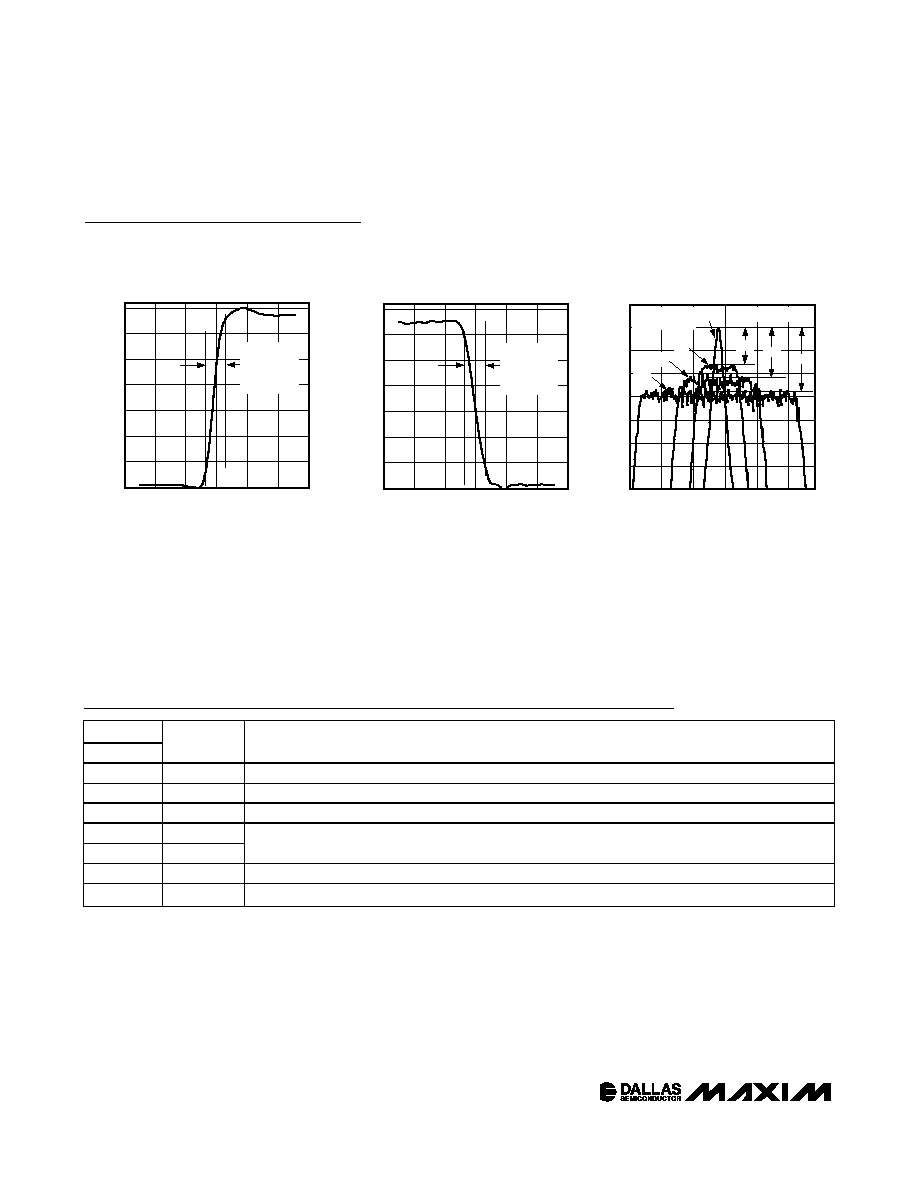
OUTPUT FALL TIME
DS1091L toc07
TIME (ns)
OUTPUT (V)
FALL TIME
= 1.13ns
TYPICAL
AT 12pF LOAD
-35
-30
-25
-20
-15
-10
-5
0
5
31.9
32.9
32.4
33.4
33.9
34.4
34.9
SPECTRUM ATTENUATION vs. FREQUENCY
AT DIFFERENT DITHER AMPLITUDES
DS1091L toc08
FREQUENCY (MHz)
ATTENUATION (dB)
0%
±1%
±2%
±4%
8dB
11dB
14dB
f
OUT
= 33.3MHz
RBW = 120kHz
CENTER DITHER
0.0
0.5
1.0
1.5
2.0
2.5
3.0
3.5
OUTPUT RISE TIME
DS1091L toc06
TIME (ns)
OUTPUT (V)
RISE TIME
= 1.02ns
TYPICAL
AT 12pF LOAD

Detailed Description
The DS1091L is a clock generator that is capable of
output frequencies from 130kHz to 66.6MHz over the
full automotive temperature range (-40∞C to +125∞C).
The device also is capable of producing a spread-
spectrum (dithered) square-wave output using four pin-
selectable dither percentages. Both center (DS1091LA)
and down (DS1091LB) dithering options are available.
The device also features two selectable dither rates.
The DS1091L is shipped from the factory programmed
to a customer-specified frequency.
Spread Spectrum
The DS1091L has the ability to reduce radiated emis-
sion peaks. The dither percentage is controlled by the
state of the SEL0 and SEL1 pins. The output frequency
can be dithered at 0%, ±1%, ±2%, and ±4%, centered
around the programmed frequency (for the DS1091LB
this can be down dithered by 0%, -2%, -4%, and -8%).
The two select pins SEL0 and SEL1 provide a means of
selecting the dither magnitudes as follows:
A triangle wave generator injects a control signal into
the master oscillator to dither its output. The dither rate
is a function of the output frequency, f
OUT
as well as the
setting of the DR pin (see the equation below). Figure 1
shows a plot of the output frequency versus time.
where n is defined in Table 2 as a function of output fre-
quency. For example, for an output frequency of
27.0MHz, the dither rate would be 13.2kHz for DR = 0
and 6.6kHz for DR = 1.
DITHER RATE
f
OUT
n
=
2
DS1091L
Automotive Temperature Range
Spread-Spectrum Econoscillator
_____________________________________________________________________
5
Block Diagram
FACTORY-PROGRAMMED
MASTER OSCILLATOR
DITHER RATE DIVIDER
TRIANGLE WAVE GENERATOR
(DITHER %)
F
ACTOR
Y
-
PROGRAMMED
PRESCALER
SEL0
SEL1
DR
OUT
f
OUT
V
CC
V
CC
GND
WHERE
f
MOSC
IS THE MASTER OSCILLATOR FREQUENCY.
f
MOSC
f
DITHER
f
MOSC
DS1091L
Table 1.
DITHER MAGNITUDE
SEL1
LOGIC LEVEL
SEL0
LOGIC LEVEL
DS1091LA
DS1091LB
0
0
No Dither
No Dither
0
1
±1%
-2%
1
0
±2%
-4%
1
1
±4%
-8%
Table 2.
OUTPUT FREQUENCY f
OUT
(MHz)
n
f
OUT
(min)
f
OUT
(max)
DR = LOGIC
LEVEL 1
DR = LOGIC
LEVEL 0
0.130
0.260
4
5
0.261
0.521
5
6
0.522
1.042
6
7
1.043
2.083
7
8
2.084
4.167
8
9
4.168
8.333
9
10
8.334
16.667
10
11
16.668
33.333
11
12
33.334
66.667
12
13