1 of 21
112801
FEATURES
ß Real-time clock (RTC) keeps track of
hundredths of seconds, minutes, hours, days,
date of the month, months, and years
ß 128k x 8 NV SRAM directly replaces
volatile static RAM or EEPROM
ß Embedded lithium energy cell maintains
calendar operation and retains RAM data
ß Watch function is transparent to RAM
operation
ß Month and year determine the number of
days in each month; valid up to 2100
ß Full 10% operating range
ß Operating temperature range: 0∞C to +70∞C
ß Over 10 years of data retention in the
absence of power
ß Lithium energy source is electrically
disconnected to retain freshness until power
is applied for the first time
ß DIP Module only
ß Standard 32-pin JEDEC pinout
ß PowerCap
Æ
Module Board only
- Surface mountable package for direct
connection to PowerCap containing
battery and crystal
- Replaceable battery (PowerCap)
- Pin for pin compatible with DS1244P
and DS1251P
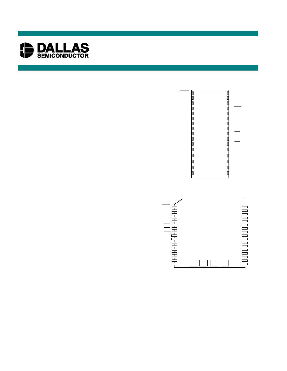
PIN ASSIGNMENT
DS1248/DS1248P
1024k NV SRAM with Phantom Clock
www.maxim-ic.com
1
RST
2
3
A15
A16
NC
V
CC
WE
OE
CE
DQ7
DQ6
DQ5
DQ4
DQ3
DQ2
DQ1
DQ0
GND
4
5
6
7
8
9
10
11
12
13
14
15
16
17
NC
A14
33
32
31
30
29
28
27
26
25
24
23
22
21
20
19
18
A13
A12
A11
A10
A9
A8
A7
A6
A5
A4
A3
A2
A1
A0
34
NC
X1 GND V
BAT
X2
34-Pin PowerCap Module Board
(Uses DS9034PCX PowerCap)
RST
13
1
2
3
4
5
6
7
8
9
10
11
12
14
31
32-Pin Encapsulated Package
740mil Flush
A14
A7
A5
A4
A3
A2
A1
A0
DQ1
DQ0
V
CC
A15
NC
WE
A13
A8
A9
A11
OE
A10
CE
DQ7
DQ5
DQ6
32
30
29
28
27
26
25
24
23
22
21
19
20
A16
A12
A6
DQ2
GND
15
16
18
17
DQ4
DQ3
PowerCap is a registered trademark of Dallas Semiconductor.
DS1248/DS1248P
2 of 21
ORDERING INFORMATION
DS1248YP≠XXXY (5V)
- IND Industrial
- 70
70ns access
blank 32-Pin DIP Module
P
34-Pin PowerCap Module board*
DS1248WP-XXXY (3.3V)
- IND Industrial
- 120 120ns access
blank 32-Pin DIP Module
P
34-Pin PowerCap Module board*
*DS9034PCX (PowerCap) Required:
(Must be ordered separately.)
PIN DESCRIPTION
A
0
≠A
16
-
Address
Inputs
CE
- Chip Enable
OE
- Output Enable
WE
- Write Enable
V
CC
- Power Supply Input
GND -
Ground
DQ
0
≠DQ
7
- Data In/Data Out
NC
- No Connection
X1, X2
- Crystal Connection
V
BAT
- Battery Connection
RST
-
Reset
DESCRIPTION
The DS1248 1024k NV SRAM with Phantom Clock is a fully static nonvolatile RAM (organized as 128k
words by 8 bits) with a built-in real-time clock. The DS1248 has a self-contained lithium energy source
and control circuitry, which constantly monitors V
CC
for an out-of-tolerance condition. When such a
condition occurs, the lithium energy source is automatically switched on and writes protection is
unconditionally enabled to prevent garbled data in both the memory and real-time clock.
PACKAGES
The DS1248 is available in two packages: 32-pin DIP and 34-pin PowerCap module. The 32-pin DIP
style module integrates the crystal, lithium energy source, and silicon in one package. The 34-pin
PowerCap module board is designed with contacts for connection to a separate PowerCap (DS9034PCX)
that contains the crystal and battery. This design allows the PowerCap to be mounted on top of the
DS1248P after completion of the surface mount process. Mounting the PowerCap after the surface mount
process prevents damage to the crystal and battery because of the high temperatures required for solder
reflow. The PowerCap is keyed to prevent reverse insertion. The PowerCap module board and PowerCap
are ordered separately and shipped in separate containers.

DS1248/DS1248P
3 of 21
RAM READ MODE
The DS1248 executes a read cycle whenever
WE
(write enable) is inactive (high) and
CE
(chip enable) is
active (low). The unique address specified by the 17 address inputs (A0≠A16) defines which of the 128k
bytes of data is to be accessed. Valid data will be available to the eight data-output drivers within t
ACC
(access time) after the last address input signal is stable, providing that
CE
and
OE
(output enable) access
times and states are also satisfied. If
OE
and
CE
access times are not satisfied, then data access must be
measured from the later occurring signal (
CE
or
OE
) and the limiting parameter is either t
CO
for
CE
or
t
OE
for
OE
, rather than address access.
RAM WRITE MODE
The DS1248 is in the write mode whenever the
WE and CE signals are in the active (low) state after
address inputs are stable. The latter occurring falling edge of CE or WE will determine the start of the
write cycle. The write cycle is terminated by the earlier rising edge of CE or WE . All address inputs
must be kept valid throughout the write cycle. WE must return to the high state for a minimum recovery
time (t
WR
) before another cycle can be initiated. The OE control signal should be kept inactive (high)
during write cycles to avoid bus contention. However, if the output bus has been enabled ( CE and OE
active) then WE will disable the outputs in t
ODW
from its falling edge.
DATA RETENTION MODE
The 5V device is fully accessible and data can be written or read only when V
CC
is greater than V
PF
.
However, when V
CC
is below the power-fail point, V
PF
(point at which write protection occurs), the
internal clock registers and SRAM are blocked from any access. When V
CC
falls below the battery switch
point, V
SO
(battery supply level), device power is switched from the V
CC
pin to the backup battery. RTC
operation and SRAM data are maintained from the battery until V
CC
is returned to nominal levels.
The 3.3V device is fully accessible and data can be written or read only when V
CC
is greater than V
PF
.
When V
CC
falls below V
PF
, access to the device is inhibited. If V
PF
is less than V
BAT
, the device power is
switched from V
CC
to the backup supply (V
BAT
) when V
CC
drops below V
PF
. If V
PF
is greater than V
BAT
,
the device power is switched from V
CC
to the backup supply (V
BAT
) when V
CC
drops below V
BAT
. RTC
operation and SRAM data are maintained from the battery until V
CC
is returned to nominal levels.
All control, data, and address signals must be powered down when V
CC
is powered-down.
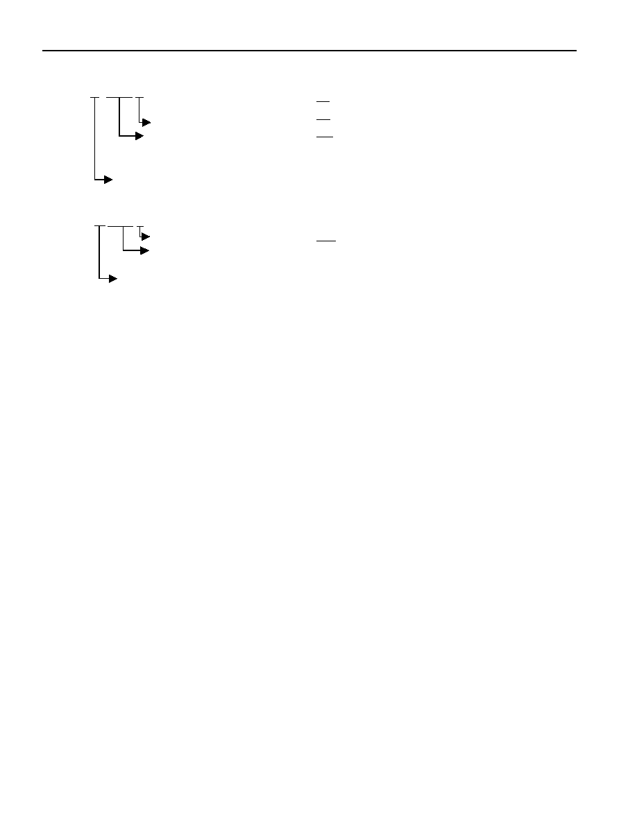
PHANTOM CLOCK OPERATION
Communication with the phantom clock is established by pattern recognition on a serial bit stream of
64 bits, which must be matched by executing 64 consecutive write cycles containing the proper data on
DQ0. All accesses that occur prior to recognition of the 64-bit pattern are directed to memory.
After recognition is established, the next 64 read or write cycles either extract or update data in the
phantom clock, and memory access is inhibited.
Data transfer to and from the timekeeping function is accomplished with a serial bit stream under control
of chip enable, output enable, and write enable. Initially, a read cycle to any memory location using the
CE
and
OE
control of the phantom clock starts the pattern recognition sequence by moving a pointer to

DS1248/DS1248P
4 of 21
the first bit of the 64-bit comparison register. Next, 64 consecutive write cycles are executed using the
CE
and
WE
control of the SmartWatch. These 64 write cycles are used only to gain access to the
phantom clock. Therefore, any address to the memory in the socket is acceptable. However, the write
cycles generated to gain access to the phantom clock are also writing data to a location in the mated
RAM. The preferred way to manage this requirement is to set aside just one address location in RAM as a
phantom clock scratch pad. When the first write cycle is executed, it is compared to bit 0 of the 64-bit
comparison register. If a match is found, the pointer increments to the next location of the comparison
register and awaits the next write cycle. If a match is not found, the pointer does not advance and all
subsequent write cycles are ignored. If a read cycle occurs at any time during pattern recognition, the
present sequence is aborted and the comparison register pointer is reset. Pattern recognition continues for
a total of 64 write cycles as described above until all the bits in the comparison register have been
matched (Figure 1). With a correct match for 64 bits, the phantom clock is enabled and data transfer to or
from the timekeeping registers can proceed. The next 64 cycles will cause the phantom clock to either
receive or transmit data on DQ0, depending on the level of the
OE
pin or the
WE
pin. Cycles to other
locations outside the memory block can be interleaved with
CE
cycles without interrupting the pattern
recognition sequence or data transfer sequence to the phantom clock.
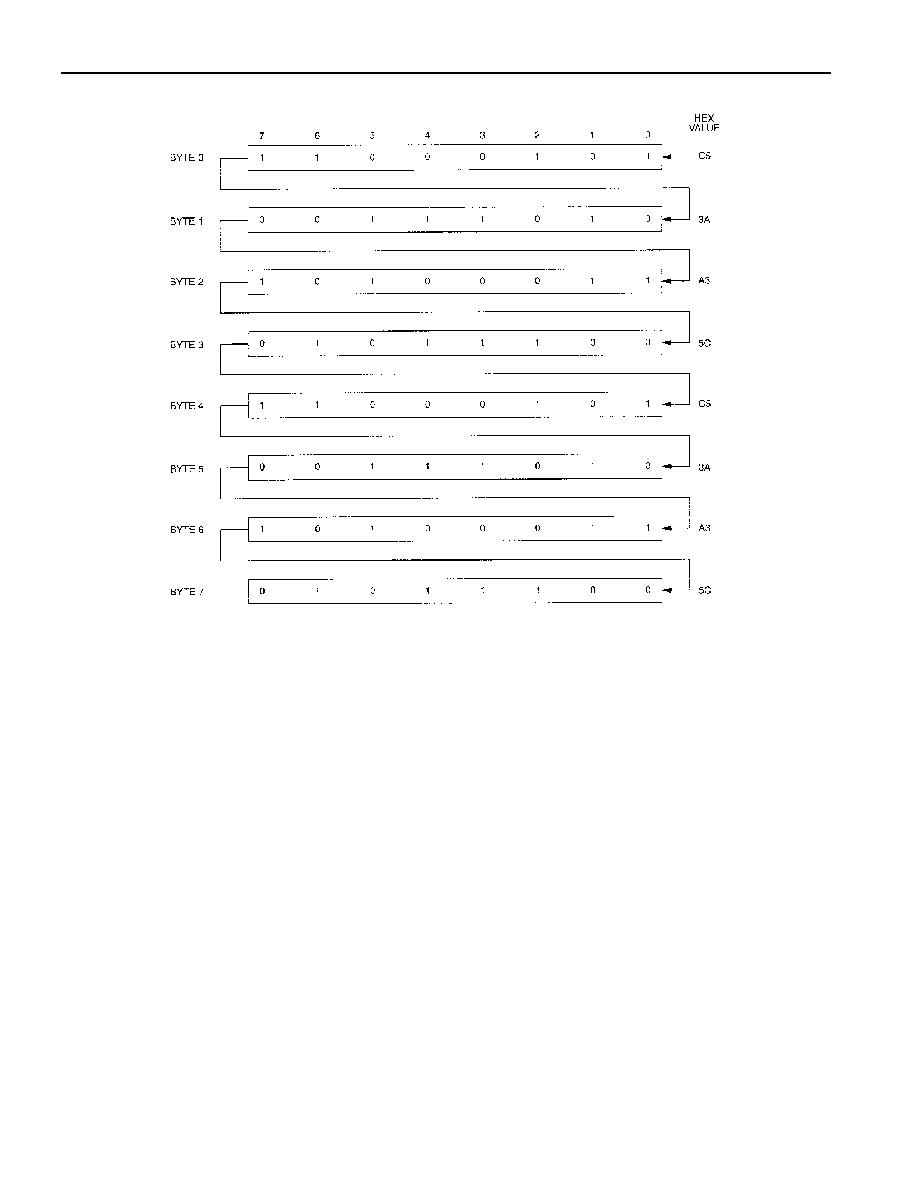
PHANTOM CLOCK REGISTER INFORMATION
The phantom clock information is contained in eight registers of 8 bits, each of which is sequentially
accessed 1 bit at a time after the 64-bit pattern recognition sequence has been completed. When updating
the phantom clock registers, each register must be handled in groups of 8 bits. Writing and reading
individual bits within a register could produce erroneous results. These read/write registers are defined in
Figure 2.
Data contained in the phantom clock register is in binary-coded decimal format (BCD). Reading and
writing the registers is always accomplished by stepping through all eight registers, starting with bit 0 of
register 0 and ending with bit 7 of register 7.
DS1248/DS1248P
5 of 21
PHANTOM CLOCK REGISTER DEFINITION Figure 1
Note: The pattern recognition in Hex is C5, 3A, A3, 5C, C5, 3A, A3, 5C. The odds of this pattern being
accidentally duplicated and causing inadvertent entry to the phantom clock is less than 1 in 10
19
. This
pattern is sent to the phantom clock LSB to MSB.