1 of 21
REV: 040203
Note: Some revisions of this device may incorporate deviations from published specifications known as errata. Multiple revisions of any device
may be simultaneously available through various sales channels. For information about device errata, click here:
www.maxim-ic.com/errata
.
DESCRIPTION
The DS1315 Phantom Time Chip is a
combination of a CMOS timekeeper and a
nonvolatile memory controller. In the absence of
power, an external battery maintains the
timekeeping operation and provides power for a
CMOS static RAM. The watch keeps track of
hundredths of seconds, seconds, minutes, hours,
day, date, month, and year information. The last
day of the month is automatically adjusted for
months with less than 31 days, including leap
year correction. The watch operates in one of two
formats: a 12-hour mode with an AM/PM
indicator or a 24-hour mode. The nonvolatile
controller supplies all the necessary support
circuitry to convert a CMOS RAM to a
nonvolatile memory. The DS1315 can be
interfaced with either RAM or ROM without
leaving gaps in memory.
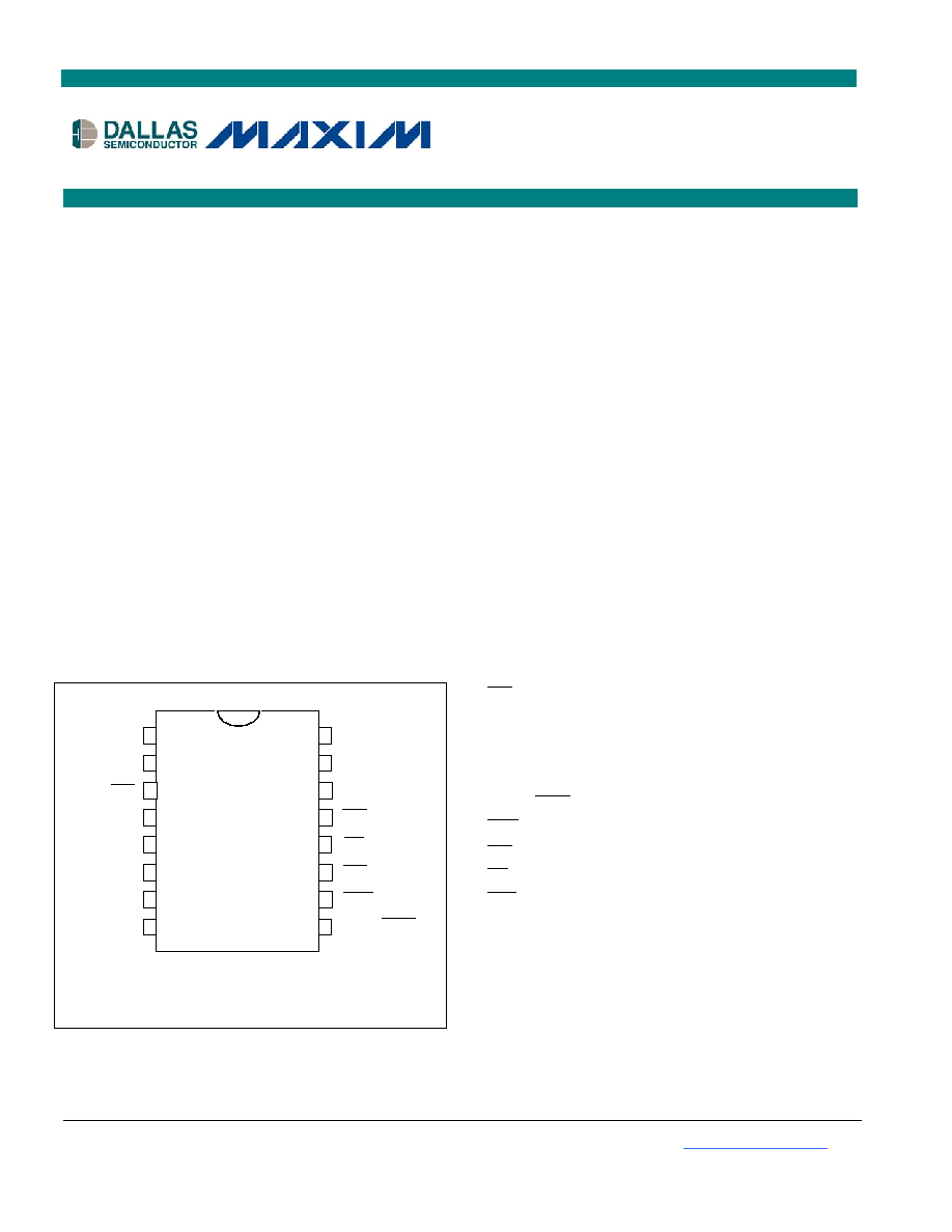
PIN CONFIGURATIONS
Pin Configurations continued at end of data sheet.
FEATURES
� Real time clock keeps track of hundredths of
seconds, seconds, minutes, hours, days, date
of the month, months, and years
� Adjusts for months with fewer than 31 days
� Automatic leap year correction valid up to
2100
� No address space required to communicate
with RTC
� Provides nonvolatile controller functions for
battery backup of SRAM
� Supports redundant battery attachment for
high�reliability applications
� Full �10% V
CC
operating range
� +3.3 volt or +5 volt operation
� Industrial (�45�C to +85�C) operating
temperature ranges available
� Drop in replacement for DS1215
PIN DESCRIPTION
X1, X2
- 32.768 kHz Crystal Connection
WE
- Write Enable
BAT1
- Battery 1 Input
GND
-
Ground
D -
Data
Input
Q
- Data Output
ROM/
RAM
- ROM/RAM Mode Select
CEO
- Chip Enable Output
CEI
- Chip Enable Input
OE
- Output Enable
RST
-
Reset
BAT2
- Battery 2 Input
V
CC0
- Switched Supply Output
V
CC1
- Power Supply Input
www.dalsemi.com
DS1315
Phantom Time Chip
www.maxim-ic.com
16-Pin DIP (300-mil)
1
2
3
4
5
6
7
8
16
15
14
13
12
11
10
9
V
CC1
V
CC0
BAT2
RST
OE
CEI
CEO
ROM/RAM
X1
X2
WE
BAT1
GND
D
Q
GND
DS1315 Phantom Time Chip
2 of 21
ORDERING INFORMATION
PART TEMP
RANGE
PIN-PACKAGE
TOP
MARK
DS1315-5
0�C to +70�C
16 DIP
DS1315 56
DS1315-33
0�C to +70�C
16 DIP
DS1315 336
DS1315N-5
-40�C to +85�C
16 DIP
DS1315 56
DS1315N-33
-40�C to +85�C
16 DIP
DS1315 336
DS1315E-5
0�C to +70�C
20 TSSOP
DS1315E
56
DS1315E-33
0�C to +70�C
20 TSSOP
DS1315E
336
DS1315EN-5
-40�C to +85�C
20 TSSOP
DS1315E
xxxxx-56
DS1315EN-33
-40�C to +85�C
20 TSSOP
DS1315E
xxxx-336
DS1315EN-33/T&R
-40�C to +85�C
20 TSSOP
DS1315E
xxxx-336
DS1315EN-5/T&R
-40�C to +85�C
20 TSSOP
DS1315E
xxxxx-56
DS1315S-5
0�C to +70�C
16 SO
DS1315S
56
DS1315S-33
0�C to +70�C
16 SO
DS1315S
336
DS1315S-5/T&R
0�C to +70�C
16 SO
DS1315S
56
DS1315SN-5
-40�C to +85�C
16 SO
DS1315S
56
DS1315SN-33
-40�C to +85�C
16 SO
DS1315S
336
Note: An "N" located in the bottom right-hand corner of the top of the package denotes an industrial device. "xxxx" can be any combination of characters.
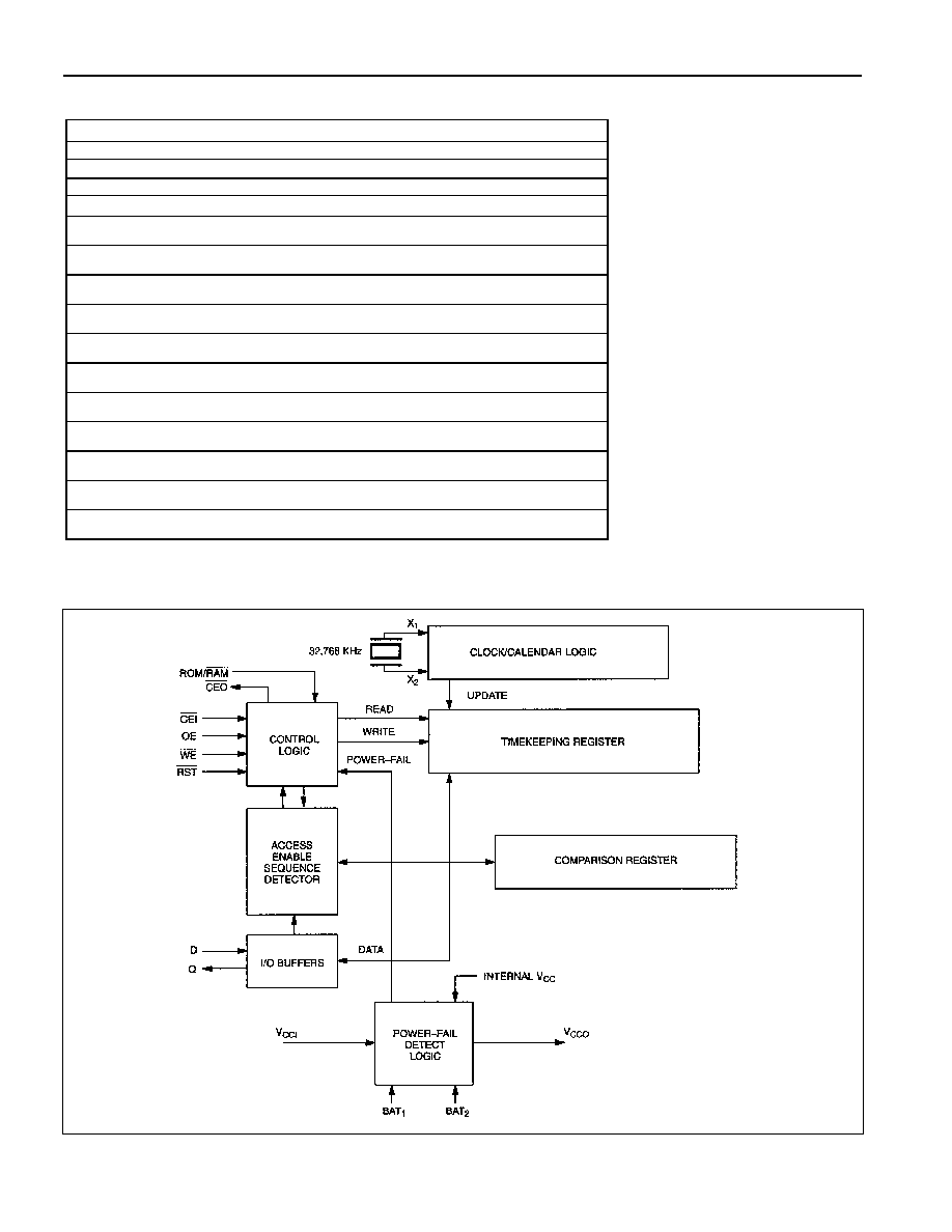
Figure 1. Block Diagram

DS1315 Phantom Time Chip
3 of 21
Operation
Communication with the Time Chip is established by pattern recognition of a serial bit stream of 64 bits
which must be matched by executing 64 consecutive write cycles containing the proper data on data in
(D). All accesses which occur prior to recognition of the 64-bit pattern are directed to memory via the
chip enable output pin (
CEO
).
After recognition is established, the next 64 read or write cycles either extract or update data in the Time
Chip and
CEO
remains high during this time, disabling the connected memory.
Data transfer to and from the timekeeping function is accomplished with a serial bit stream under control
of chip enable input (
CEI
), output enable (
OE
), and write enable (
WE
). Initially, a read cycle using the
CEI
and
OE
control of the Time Chip starts the pattern recognition sequence by moving pointer to the
first bit of the 64-bit comparison register. Next, 64 consecutive write cycles are executed using the
CEI
and
WE
control of the Time Chip. These 64 write cycles are used only to gain access to the Time Chip.
When the first write cycle is executed, it is compared to bit 1 of the 64-bit comparison register. If a match
is found, the pointer increments to the next location of the comparison register and awaits the next write
cycle. If a match is not found, the pointer does not advance and all subsequent write cycles are ignored. If
a read cycle occurs at any time during pattern recognition, the present sequence is aborted and the
comparison register pointer is reset. Pattern recognition continues for a total of 64 write cycles as
described above until all the bits in the comparison register have been matched. (This bit pattern is shown
in Figure 2). With a correct match for 64 bits, the Time Chip is enabled and data transfer to or from the
timekeeping registers may proceed. The next 64 cycles will cause the Time Chip to either receive data on
D, or transmit data on Q, depending on the level of
OE
pin or the
WE
pin. Cycles to other locations
outside the memory block can be interleaved with
CEI
cycles without interrupting the pattern recognition
sequence or data transfer sequence to the Time Chip.
A standard 32.768 kHz quartz crystal can be directly connected to the DS1315 via pins 1 and 2 (X1, X2).
The crystal selected for use should have a specified load capacitance (C
L
) of 6 pF. For more information
on crystal selection and crystal layout considerations, please consult Application Note 58, "Crystal
Considerations with Dallas Real Time Clocks."
DS1315 Phantom Time Chip
4 of 21
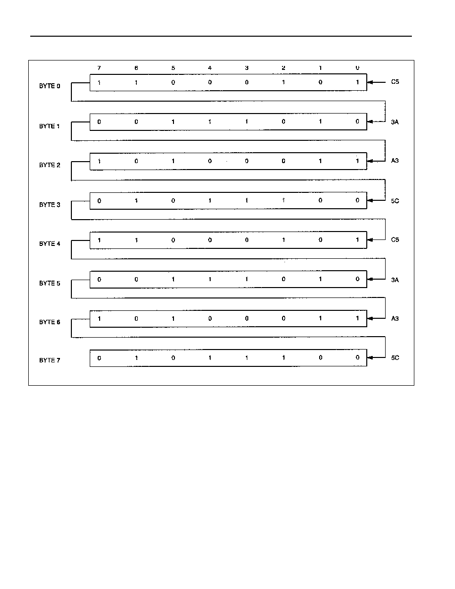
Figure 2. Time Chip Comparison Register Definition
Note: The pattern recognition in Hex is C5, 3A, A3, 5C, C5, 3A, A3, 5C. The odds of this pattern being
accidentally duplicated and causing inadvertent entry to the Phantom Time Chip are less than 1 in 10
19
.
DS1315 Phantom Time Chip
5 of 21
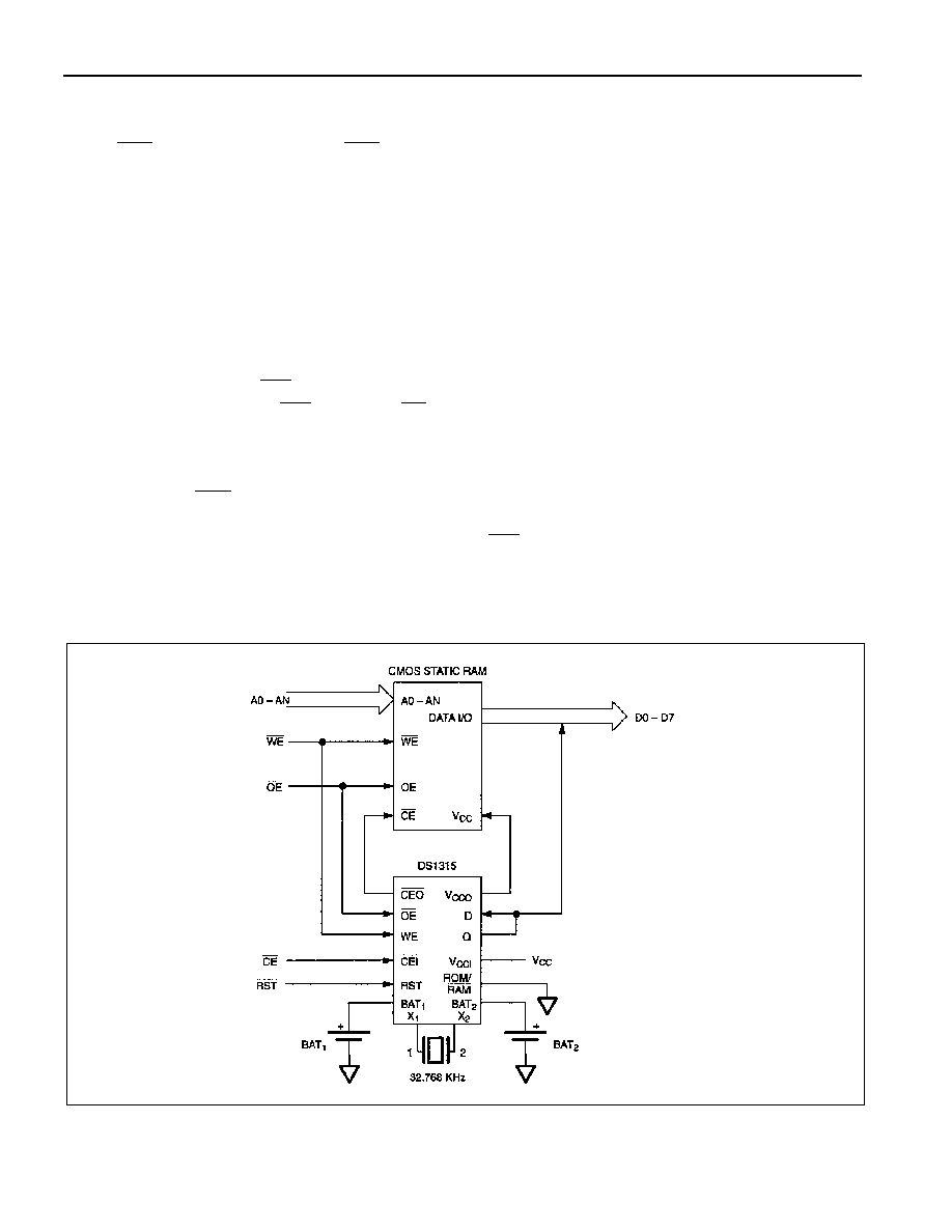
Nonvolatile Controller Operation
The operation of the nonvolatile controller circuits within the Time Chip is determined by the level of the
ROM/
RAM
select pin. When ROM/
RAM
is connected to ground, the controller is set in the RAM mode
and performs the circuit functions required to make CMOS RAM and the timekeeping function
nonvolatile. A switch is provided to direct power from the battery inputs or V
CCI
to V
CCO
with a
maximum voltage drop of 0.3 volts. The V
CCO
output pin is used to supply uninterrupted power to CMOS
SRAM. The DS1315 also performs redundant battery control for high reliability. On power-fail, the
battery with the highest voltage is automatically switched to V
CCO
. If only one battery is used in the
system, the unused battery input should be connected to ground.
The DS1315 safeguards the Time Chip and RAM data by power-fail detection and write protection.
Power-fail detection occurs when V
CCI
falls below V
PF
which is set by an internal bandgap reference. The
DS1315 constantly monitors the V
CCI
supply pin. When V
CCI
is less than V
PF
, power-fail circuitry forces
the chip enable output (
CEO
) to V
CCI
or V
BAT
-0.2 volts for external RAM write protection. During
nominal supply conditions,
CEO
will track
CEI
with a propagation delay. Internally, the DS1315 aborts
any data transfer in progress without changing any of the Time Chip registers and prevents future access
until V
CCI
exceeds V
PF
. A typical RAM/Time Chip interface is illustrated in Figure 3.
When the ROM/
RAM
pin is connected to V
CCO
, the controller is set in the ROM mode. Since ROM is a
read-only device that retains data in the absence of power, battery backup and write protection is not
required. As a result, the chip enable logic will force
CEO
low when power fails. However, the Time
Chip does retain the same internal nonvolatility and write protection as described in the RAM mode. A
typical ROM/Time Chip interface is illustrated in Figure 4.
Figure 3. DS1315-to-RAM/Time Chip Interface