 | –≠–ª–µ–∫—Ç—Ä–æ–Ω–Ω—ã–π –∫–æ–º–ø–æ–Ω–µ–Ω—Ç: DS1338-3 | –°–∫–∞—á–∞—Ç—å:  PDF PDF  ZIP ZIP |
1 of 16 010803
Note: Some revisions of this device may incorporate deviations from published specifications known as errata. Multiple revisions of any device
may be simultaneously available through various sales channels. For information about device errata, click here:
www.maxim-ic.com/errata
.
GENERAL DESCRIPTION
The DS1338 serial real-time clock (RTC) is a low-
power, full binary-coded decimal (BCD)
clock/calendar plus 56 Bytes of NV SRAM. Address
and data are transferred serially through a 2-wire
bidirectional bus. The clock/calendar provides
seconds, minutes, hours, day, date, month, and year
information. The end of the month date is
automatically adjusted for months with fewer than 31
days, including corrections for leap year. The clock
operates in either the 24-hour or 12-hour format with
AM/PM indicator. The DS1338 has a built-in power-
sense circuit that detects power failures and
automatically switches to the battery supply.
APPLICATIONS
Handhelds (GPS, POS Terminal)
Consumer Electronics (Set-Top Box, Digital
Recording, Network Appliance)
Office Equipment (Fax/Printer, Copier)
Medical (Glucometer, Medicine Dispenser)
Telecommunications (Router, Switcher, Server)
Other (Utility Meter, Vending Machine, Thermostat,
Modem)
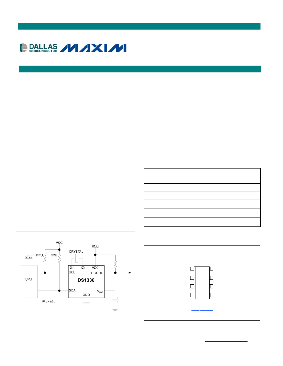
TYPICAL OPERATING CIRCUIT
FEATURES
ß
RTC Counts Seconds, Minutes, Hours, Date of the
Month, Month, Day of the Week, and Year with
Leap-Year Compensation Valid Up to 2100
ß
56-Byte Battery-Backed NV RAM for Data
Storage
ß
2-Wire Serial Interface
ß
Programmable Square-Wave Output Signal
ß
Automatic Power-Fail Detect and Switch
Circuitry
ß
Consumes Less than 500nA in Battery-Backup
Mode with Oscillator Running
ß
Recognized by Underwriters Laboratory (UL)
ORDERING INFORMATION
PART TEMP
RANGE
PIN-PACKAGE
TOP
MARK
DS1338Z-18
-40∞C to +85∞C 8 SO (150mil)
DS1338-18
DS1338Z-3
-40∞C to +85∞C 8 SO (150mil)
DS1338-3
DS1338Z-33
-40∞C to +85∞C 8 SO (150mil)
DS1338-33
DS1338U-18
-40∞C to +85∞C
8
mSOP
1338
rr-18
DS1338U-3
-40∞C to +85∞C
8
mSOP
1338
rr-3
DS1338U-33
-40∞C to +85∞C
8
mSOP
1338
rr-33
rr = revision level
PIN CONFIGURATION
DS1338
2-Wire RTC with 56-Byte NV RAM
www.maxim-ic.com
SO,
µSOP
SQW/OUT
1
2
3
4
8
7
6
5
X1
X2
V
BAT
GND
V
CC
SCL
SDA
TOP VIEW
DS1338
2 of 16
ABSOLUTE MAXIMUM RATINGS
Voltage Range on Any Pin Relative to Ground
-0.3V to +6.0V
Operating Temperature Range
-40∞C to +85∞C
Storage Temperature Range
-55∞C to +125∞C
Soldering Temperature
See IPC/JEDEC J-STD-020A
Stresses beyond those listed under "Absolute Maximum Ratings" may cause permanent damage to the device. These are stress ratings only,
and functional operation of the device at these or any other conditions beyond those indicated in the operational sections of the specifications is
not implied. Exposure to the absolute maximum rating conditions for extended periods may affect device.
RECOMMENDED DC OPERATING CONDITIONS
(V
CC
= V
CC
MIN
to V
CC
MAX
, T
A
= -40∞C to +85∞C.) (Note 1)
PARAMETER SYMBOL
CONDITIONS
MIN TYP
MAX
UNITS
DS1338-18 1.71
1.8
1.89
DS1338-3 2.7
3.0
3.3
Supply Voltage
V
CC
DS1338-33 3.0
3.3
3.63
V
Logic 1
V
IH
(Note
2)
0.7
V
CC
V
CC
+ 0.3
Logic 0
V
IL
(Note
2)
-0.3
0.3
V
CC
DS1338-18 1.51
1.62
1.71
DS1338-3 2.45
2.59
2.70
Power-Fail Voltage
V
PF
DS1338-33 2.70
2.82
2.97
V
V
BAT
Battery Voltage
V
BAT
(Note
2)
1.3
3.0
3.7
V
DC ELECTRICAL CHARACTERISTICS
(V
CC
= V
CC
MIN
to V
CC
MAX
, T
A
= -40∞C to +85∞C.) (Note 1)
PARAMETER SYMBOL
CONDITIONS
MIN
TYP
MAX
UNITS
V
BAT
Battery Voltage
V
BAT
(Note
2)
1.3
3.7
V
Input Leakage
I
LI
(Note
3)
1
mA
I/O Leakage
I
LO
(Note
4)
1
mA
V
CC
> 2V; V
OL
= 0.4V
3.0
SDA Logic 0 Output
I
OLSDA
V
CC
< 2V; V
OL
= 0.2 V
CC
3.0
mA
V
CC
> 2V; V
OL
= 0.4V
3.0
1.71V < V
CC
< 2V;
V
OL
= 0.2 V
CC
3.0
mA
SQW/OUT Logic 0 Output
I
OLSQW
1.3V < V
CC
< 1.71V;
V
OL
= 0.2 V
CC
250
mA
DS1338-18
75
150
DS1338-3
110
200
Active Supply Current
(Note 5)
I
CCA
DS1338-33
120
200
mA
DS1338-18
60
100
DS1338-3
80
125
Standby Current (Note 6)
I
CCS
DS1338-33
85
125
mA
V
BAT
Leakage Current
(V
CC
Active)
I
BATLKG
25 100
nA
DS1338
3 of 16
DC ELECTRICAL CHARACTERISTICS
(V
CC
= 0V, T
A
= -40∞C to +85∞C.) (Note 1)
PARAMETER SYMBOL
MIN
TYP
MAX
UNITS
Oscillator Current (OSC ON); V
BAT
= 3.7V,
SQW/OUT OFF (Note 7)
I
BATOSC1
400
1200
nA
Oscillator Current (OSC ON); V
BAT
= 3.7V,
SQW/OUT ON (32kHz) (Note 7)
I
BATOSC2
570
1400
nA
V
BAT
Data-Retention Current; V
BAT
= 3.7V
(Oscillator Off, V
CC
= 0.0V)
I
BATDAT
10 100 nA
CRYSTAL SPECIFICATIONS
*
PARAMETER SYMBOL
MIN
TYP
MAX
UNITS
Nominal Frequency
f
O
32.768
kHz
Series Resistance
ESR
45
k
Load Capacitance
C
L
12.5
pF
*The crystal, traces, and crystal input pins should be isolated from RF generating signals. Refer to Application Note 58: Crystal Considerations
for Dallas Real-Time Clocks for additional specifications.
DS1338
4 of 16
AC ELECTRICAL CHARACTERISTICS
(T
A
= -40∞C to +85∞C) (Note 1)
PARAMETER SYMBOL
CONDITION
MIN
TYP MAX UNITS
Fast mode
100
400
SCL Clock Frequency
f
SCL
Standard mode
100
kHz
Fast mode
1.3
Bus Free Time Between STOP
and START Condition
t
BUF
Standard mode
4.7
ms
Fast mode
0.6
Hold Time (Repeated) START
Condition (Note 8)
t
HD:STA
Standard mode
4.0
ms
Fast mode
1.3
LOW Period of SCL Clock
t
LOW
Standard mode
4.7
ms
Fast mode
0.6
HIGH Period of SCL Clock
t
HIGH
Standard mode
4.0
ms
Fast mode
0.6
Setup Time for Repeated START
Condition
t
SU:STA
Standard mode
4.7
ms
Fast mode
0
0.9
Data Hold Time (Notes 9, 10)
t
HD:DAT
Standard mode
0
ms
Fast mode
100
Data Setup Time (Note 11)
t
SU:DAT
Standard mode
250
ns
Fast mode
20 +
0.1C
B
300
Rise Time of Both SDA and SCL
Signals (Note 12)
t
R
Standard mode
1000
ns
Fast mode
20 +
0.1C
B
300
Fall Time of Both SDA and SCL
Signals (Note 12)
t
F
Standard mode
300
ns
Fast mode
0.6
Setup Time for STOP Condition
t
SU:STO
Standard mode
4.0
ms
Capacitive Load for Each Bus
Line (Note 12)
C
B
400
pF
I/O Capacitance
C
I/O
10
pF
Oscillator Stop Flag (OSF) Delay
(Note 13)
t
OSF
100 ms

DS1338
5 of 16
POWER-UP/POWER-DOWN CHARACTERISTICS
(T
A
= -40∞C to +85∞C) (Note 1)
PARAMETER SYMBOL
MIN
TYP
MAX
UNITS
Recovery at Power-Up (Note 14)
t
REC
2
ms
V
CC
Fall Time; V
PF(MAX)
to V
PF(MIN)
t
VCCF
300
ms
V
CC
Rise Time; V
PF(MIN)
to V
PF(MAX)
t
VCCR
0
ms
Note 1: Limits at -40∞C are guaranteed by design and not production tested.
Note 2: All voltages are referenced to ground.
Note 3: SCL only.
Note 4: SDA and SQW/OUT.
Note 5: I
CCA
--SCL clocking at max frequency = 400kHz.
Note 6: Specified with 2-wire bus inactive.
Note 7: Measured with a 32.768kHz crystal attached to X1 and X2.
Note 8: After this period, the first clock pulse is generated.
Note 9: A device must internally provide a hold time of at least 300ns for the SDA signal (referred to the V
IHMIN
of the SCL signal) to bridge the
undefined region of the falling edge of SCL.
Note 10: The maximum t
HD:DAT
has only to be met if the device does not stretch the LOW period (t
LOW
) of the SCL signal.
Note 11: A fast mode device can be used in a standard mode system, but the requirement t
SU:DAT
to 250ns must then be met. This is
automatically the case if the device does not stretch the LOW period of the SCL signal. If such a device does stretch the LOW period
of the SCL signal, it must output the next data bit to the SDA line t
R MAX
+ t
SU:DAT
= 1000 + 250 = 1250ns before the SCL line is released.
Note 12: C
B
--total capacitance of one bus line in pF.
Note 13: The parameter t
OSF
is the time period the oscillator must be stopped for the OSF flag to be set over the voltage range of
0.0V V
CC
V
CC MAX
and 1.3V V
BAT
3.7V.
Note 14: This delay applies only if the oscillator is enabled and running. If the oscillator is disabled or stopped, no power-up delay occurs.