General Description
The DS1340 is a real-time clock (RTC)/calendar that is
pin compatible and functionally equivalent to the ST
M41T00, including the software clock calibration. The
device additionally provides trickle-charge capability
on the V
BACKUP
pin, a lower timekeeping voltage, and
an oscillator STOP flag. Block access of the register
map is identical to the ST device. Two additional regis-
ters, which are accessed individually, are required for
the trickle charger and flag. The clock/calendar pro-
vides seconds, minutes, hours, day, date, month, and
year information. A built-in power-sense circuit detects
power failures and automatically switches to the back-
up supply. The device is programmed serially through
an I
2
C
TM
bidirectional bus.
Applications
Portable Instruments
Point-of-Sale Equipment
Medical Equipment
Telecommunications
Features
Enhanced Second Source for the ST M41T00
Available in a Surface-Mount Package with an
Integrated Crystal (DS1340C)
Fast (400kHz) I
2
C Interface
Software Clock Calibration
RTC Counts Seconds, Minutes, Hours, Day, Date,
Month, and Year
Automatic Power-Fail Detect and Switch Circuitry
Trickle-Charge Capability
Low Timekeeping Voltage Down to 1.3V
Three Operating Voltage Ranges (1.8V, 3V, and 3.3V)
Oscillator Stop Flag
Available in 8-Pin µSOP or SO Packages
Underwriters Laboratory (UL) Recognized
DS1340
I
2
C RTC with Trickle Charger
______________________________________________ Maxim Integrated Products
1
Ordering Information
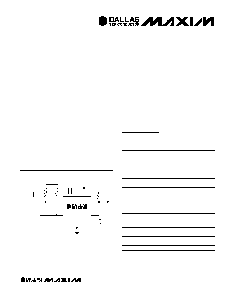
4
CPU
V
CC
V
CC
V
CC
5
6
8
1
2
SDA
SCL
GND
X2
X1
V
CC
RPU
RPU
CRYSTAL
FT/OUT
V
BACKUP
3
7
RPU = t
R
/ C
B
DS1340
Typical Operating Circuit
Rev 2; 12/04
For pricing, delivery, and ordering information, please contact Maxim/Dallas Direct! at
1-888-629-4642, or visit Maxim's website at www.maxim-ic.com.
PART
TEMP RANGE
PIN-PACKAGE
TOP
MARK
DS1340Z-18
-40∞C to +85∞C
8 SO (0.150in)
D1340-18
DS1340Z-3
-40∞C to +85∞C
8 SO (0.150in)
DS1340-3
DS1340Z-33
-40∞C to +85∞C
8 SO (0.150in)
D1340-33
DS1340U-18
-40∞C to +85∞C
8 µSOP
1340
A1-18
DS1340U-3
-40∞C to +85∞C
8 µSOP
1340
A1-3
DS1340U-33
-40∞C to +85∞C
8 µSOP
1340
A1-33
DS1340C-18
-40∞C to +85∞C
16 SO
1340C-18
DS1340C-3
-40∞C to +85∞C
16 SO
1340C-3
DS1340C-33
-40∞C to +85∞C
16 SO
1340C-33
DS1340Z-18+
-40∞C to +85∞C
8 SO (0.150in)
D1340-18
DS1340Z-3+
-40∞C to +85∞C
8 SO (0.150in)
DS1340-3
DS1340Z-33+
-40∞C to +85∞C
8 SO (0.150in)
D1340-33
DS1340U-18+
-40∞C to +85∞C
8 µSOP
1340
A1-18
DS1340U-3+
-40∞C to +85∞C
8 µSOP
1340
A1-3
DS1340U-33+
-40∞C to +85∞C
8 µSOP
1340
A1-33
DS1340C-18+
-40∞C to +85∞C
16 SO
1340C-18
DS1340C-3+
-40∞C to +85∞C
16 SO
1340C-3
DS1340C-33+
-40∞C to +85∞C
16 SO
1340C-33
I
2
C is a trademark of Philips Corp. Purchase of I
2
C compo-
nents from Maxim Integrated Products, Inc., or one of its subli-
censed Associated Companies, conveys a license under the
Philips I
2
C Patent Rights to use these components in an I
2
C
system, provided that the system conforms to the I
2
C Standard
Specification as defined by Philips.
Note: A "+" in the part number and a "+" anywhere on the top
mark indicates a lead-free device.
Pin Configurations appear at end of data sheet.
DS1340
I
2
C RTC with Trickle Charger
2
_____________________________________________________________________
ABSOLUTE MAXIMUM RATINGS
Stresses beyond those listed under "Absolute Maximum Ratings" may cause permanent damage to the device. These are stress ratings only, and functional
operation of the device at these or any other conditions beyond those indicated in the operational sections of the specifications is not implied. Exposure to
absolute maximum rating conditions for extended periods may affect device reliability.
Voltage Range on V
CC
Pin Relative to Ground .....-0.3V to +6.0V
Voltage Range on SDA, SCL, and FT/OUT
Relative to Ground..................................-0.3V to (V
CC
+ 0.3V)
Operating Temperature Range ...........................-40∞C to +85∞C
Storage Temperature Range .............................-55∞C to +125∞C
Soldering Temperature Range............................See IPC/JEDEC
J-STD-020 Specification
AC ELECTRICAL CHARACTERISTICS
(V
CC
= V
CC MIN
to V
CC MAX
, T
A
= -40∞C to +85∞C, unless otherwise noted.) (Note 1, Figure 1)
PARAMETER
SYMBOL
CONDITIONS
MIN
TYP
MAX
UNITS
Standard mode
0
100
SCL Clock Frequency
f
SCL
Fast mode
100
400
kHz
Standard mode
4.7
Bus Free Time Between STOP
and START Conditions
t
BUF
Fast mode
1.3
µs
Standard mode
4.0
Hold Time (Repeated) START
Condition (Note 2)
t
HD:STA
Fast mode
0.6
µs
Standard mode
4.7
Low Period of SCL Clock
t
LOW
Fast mode
1.3
µs
Standard mode
4.0
High Period of SCL Clock
t
HIGH
Fast mode
0.6
µs
Standard mode
0
0.9
Data Hold Time (Notes 3, 4)
t
HD:DAT
Fast mode
0
0.9
µs
Standard mode
250
Data Setup Time (Note 5)
t
SU:DAT
Fast mode
100
ns
Standard mode
4.7
START Setup Time
t
SU:STA
Fast mode
0.6
µs
Standard mode
20 + 0.1C
B
1000
Rise Time of SDA and SCL
Signals (Note 6)
t
R
Fast mode
20 + 0.1C
B
300
ns
Standard mode
20 + 0.1C
B
300
Fall Time of SDA and SCL Signals
(Note 6)
t
F
Fast mode
20 + 0.1C
B
300
ns
Standard mode
4.7
Setup Time for STOP Condition
t
SU:STO
Fast mode
0.6
µs
Capacitive Load for Each Bus
Line
C
B
(Note 6)
400
pF
I/O Capacitance (SCL, SDA)
C
I/O
10
pF
Pulse Width of Spikes that Must
be Suppressed by the Input Filter
t
SP
Fast mode
30
ns
Oscillator Stop Flag (OSF) Delay
t
OSF
(Note 7)
100
ms
DS1340
I
2
C RTC with Trickle Charger
_____________________________________________________________________
3
RECOMMENDED DC OPERATING CONDITIONS
(V
CC
= V
CC MIN
to V
CC MAX
, T
A
= -40∞C to +85∞C, unless otherwise noted. Typical values are at V
CC
= 3.3V, T
A
= +25∞C, unless
otherwise noted.) (Note 1)
PARAMETER
SYMBOL
CONDITIONS
MIN
TYP
MAX
UNITS
DS1340-18
1.71
1.8
1.89
DS1340-3
2.7
3.0
3.3
Supply Voltage (Note 8)
V
CC
DS1340-33
2.97
3.3
5.5
V
Input Logic 1 (SDA, SCL)
V
IH
(Note 8)
0.7 x V
CC
V
CC
+ 0.3
V
Input Logic 0 (SDA, SCL)
V
IL
(Note 8)
-0.3
+0.3 x V
CC
V
Supply Voltage, Pullup
(FT/OUT, SDA, SCL), V
CC
= 0V
V
PU
(Note 8)
5.5
V
DS1340-18
1.3
3.7
DS1340-3
1.3
3.7
Backup Supply Voltage (Note 8)
V
BACKUP
DS1340-33
1.3
5.5
V
R1
(Notes 9, 10)
250
R2
(Note 11)
2000
Trickle-Charge Current-Limiting
Resistors
R3
(Note 12)
4000
DS1340-18
1.51
1.6
1.71
DS1340-3
2.45
2.6
2.7
Power-Fail Voltage (Note 8)
V
PF
DS1340-33
2.70
2.88
2.97
V
Input Leakage (SCL, CLK)
I
LI
-1
+1
µA
I/O Leakage (SDA, FT/OUT)
I
LO
-1
+1
µA
V
CC
> 2V; V
OL
= 0.4V
3.0
SDA Logic 0 Output
I
OLSDA
1.7V < V
CC
< 2V; V
OL
= 0.2 x V
CC
3.0
mA
V
CC
> 2V; V
OL
= 0.4V
3.0
1.7V < V
CC
< 2V; V
OL
= 0.2 x V
CC
3.0
mA
FT/OUT Logic 0 Output
I
OLSQW
1.3V < V
CC
< 1.7V; V
OL
= 0.2x V
CC
250
µA
DS1340-18
72
150
DS1340-3
108
200
Active Supply Current (Note 13)
I
CCA
DS1340-33
192
300
µA
DS1340-18
60
100
DS1340-3
81
125
Standby Current (Note 14)
I
CCS
DS1340-33
100
150
µA
V
BACKUP
Leakage Current
I
BACKUPLKG
V
BACKUP
= 3.7V
100
nA
DC ELECTRICAL CHARACTERISTICS
(V
CC
= 0V, V
BACKUP
= 3.7V, T
A
= -40∞C to +85∞C, unless otherwise noted.) (Note 1)
PARAMETER
SYMBOL
CONDITIONS
MIN
TYP
MAX
UNITS
I
BACKUP1
OSC ON, FT = 0 (Note 15)
800
1150
I
BACKUP2
OSC ON, FT = 1 (Note 15)
850
1250
V
BACKUP
Current
I
BACKUP3
OSC ON, FT = 0, V
BACKUP
= 3.0V,
T
A
= +25∞C (Notes 15, 16)
800
1000
nA
V
BACKUP
Data-Retention Current
I
BACKUPDR
OSC OFF
25.0
100
nA
DS1340
I
2
C RTC with Trickle Charger
4
_____________________________________________________________________
POWER-UP/POWER-DOWN CHARACTERISTICS
(T
A
= -40∞C to +85∞C) (Figure 2)
PARAMETER
SYMBOL
CONDITIONS
MIN
TYP
MAX
UNITS
Recovery at Power-Up
t
REC
(Note 17)
2
ms
V
CC
Fall Time; V
PF(MAX)
to
V
PF(MIN)
t
VCCF
300
µs
V
CC
Rise Time; V
PF(MIN)
to
V
PF(MAX)
t
VCCR
0
µs
WARNING: Under no circumstances are negative undershoots, of any amplitude, allowed when device is in battery-backup mode.
Note 1:
Limits at -40∞C are guaranteed by design and not production tested.
Note 2:
After this period, the first clock pulse is generated.
Note 3:
A device must internally provide a hold time of at least 300ns for the SDA signal (referred to as the V
IH(MIN)
of the SCL
signal) to bridge the undefined region of the falling edge of SCL.
Note 4:
The maximum t
HD:DAT
only has to be met if the device does not stretch the low period (t
LOW
) of the SCL signal.
Note 5:
A fast-mode device can be used in a standard-mode system, but the requirement t
SU:DAT
to 250ns must be met. This
is automatically the case if the device does not stretch the low period of the SCL signal. If such a device does stretch the
low period of the SCL signal, it must output the next data bit to the SDA line t
R MAX
+ t
SU:DAT
= 1000 + 250 = 1250ns
before the SCL line is released.
Note 6:
C
B
--total capacitance of one bus line in pF.
Note 7:
The parameter t
OSF
is the period of time the oscillator must be stopped for the OSF flag to be set over the 0V V
CC
V
CCMAX
and 1.3V V
BAT
3.7V range.
Note 8:
All voltages are referenced to ground.
Note 9:
Measured at V
CC
= typ, V
BACKUP
= 0V, register 08h = A5h.
Note 10:
The use of the 250 trickle-charge resistor is not allowed at V
CC
> 3.63V and should not be enabled.
Note 11:
Measured at V
CC
= typ, V
BACKUP
= 0V, register 08h = A6h.
Note 12:
Measured at V
CC
= typ, V
BACKUP
= 0V, register 08h = A7h.
Note 13:
I
CCA
--SCL clocking at max frequency = 400kHz.
Note 14:
Specified with I
2
C bus inactive.
Note 15:
Measured with a 32.768kHz crystal attached to the X1 and X2 pins.
Note 16:
Limits at +25∞C are guaranteed by design and not production tested.
Note 17:
This delay applies only if the oscillator is enabled and running. If the oscillator is disabled or stopped, no power-up delay
occurs.
SDA
SCL
t
HD:STA
t
LOW
t
HIGH
t
R
t
F
t
BUF
t
HD:DAT
t
SU:DAT
REPEATED
START
t
SU:STA
t
HD:STA
t
SU:STO
t
SP
STOP
START
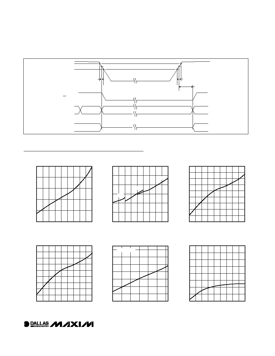
Figure 1. Data Transfer on I
2
C Serial Bus
DS1340
I
2
C RTC with Trickle Charger
_____________________________________________________________________
5
OUTPUTS
V
CC
V
PF(MAX)
INPUTS
HIGH-Z
RST
DON'T CARE
VALID
RECOGNIZED
RECOGNIZED
VALID
V
PF(MIN)
tRST
tRPU
tR
tF
V
PF
V
PF
Figure 2. Power-Up/Power-Down Timing
I
CCSA
vs. V
CC
FT = 0
DS1340 toc01
V
CC
(V)
SUPPLY CURRENT (
µ
A)
5.0
4.5
4.0
3.5
3.0
2.5
2.0
1.5
50
100
150
200
250
0
1.0
5.5
25
50
75
100
125
150
0
I
CCS
vs. V
CC
FT = 0
DS1340 toc02
V
CC
(V)
SUPPLY CURRENT (
µ
A)
5.0
4.5
4.0
3.5
3.0
2.5
2.0
1.5
1.0
5.5
-1.8V
-3.0V
-3.3V
I
BACKUP1
(FT = 0) vs. V
BACKUP
DS1340 toc03
450
500
550
600
650
700
750
800
850
400
V
BACKUP
(V)
SUPPLY CURRENT (nA)
5.0
4.5
4.0
3.5
3.0
2.5
2.0
1.5
1.0
5.5
Typical Operating Characteristics
(V
CC
= +3.3V, T
A
= +25∞C, unless otherwise noted.)
I
BACKUP2
(FT = 1) vs. V
BACKUP
DS1340 toc04
450
500
550
600
650
700
750
800
850
400
V
BACKUP
(V)
SUPPLY CURRENT (nA)
5.0
4.5
4.0
3.5
3.0
2.5
2.0
1.5
1.0
5.5
FT vs. V
BACKUP
DS1340 toc06
V
BACKUP
(V)
FREQUENCY (Hz)
5.0
4.5
1.5 2.0 2.5
3.5
3.0
4.0
511.9965
511.9970
511.9975
511.9980
511.9985
511.9990
511.9995
512.0000
511.9960
1.0
5.5
I
BACKUP3
vs. TEMPERATURE
DS1340 toc05
TEMPERATURE (∞C)
SUPPLY CURRENT (nA)
60
40
-20
0
20
500
550
600
650
700
750
800
850
-40
80
V
BACKUP
= 3.0V