 | ÐлекÑÑоннÑй компоненÑ: DS1371U | СкаÑаÑÑ:  PDF PDF  ZIP ZIP |
Äîêóìåíòàöèÿ è îïèñàíèÿ www.docs.chipfind.ru
1 of 14
REV: 051203
Note: Some revisions of this device may incorporate deviations from published specifications known as errata. Multiple revisions of any device
may be simultaneously available through various sales channels. For information about device errata, click here:
www.maxim-ic.com/errata
.
General Description
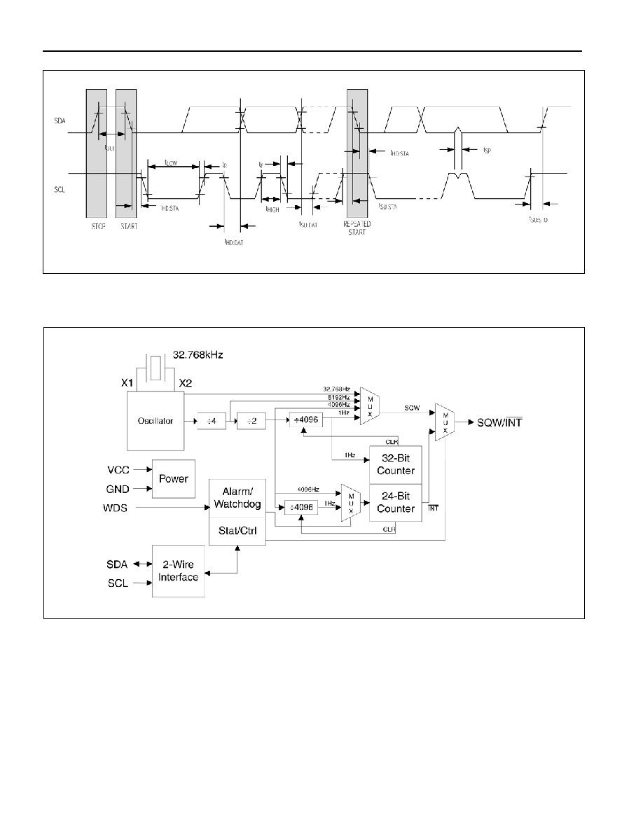
The DS1371 is a 32-bit binary counter that is
designed to continuously count time in seconds.
An additional counter that can generate a
periodic alarm or serve as a watchdog timer is
also provided. If enabled as a watchdog timer,
the watchdog strobe input pin provides a
hardware reset of the counter. If disabled, this
counter can be used as 3 Bytes of general-
purpose RAM. A configurable output can be
used as an interrupt or provide a square wave at
one of four selectable frequencies. The device is
programmed serially through a 2-wire
bidirectional bus.
Applications
Servers
Point-of-Sale Equipment
Portable Instruments
Elapsed Time Measurements
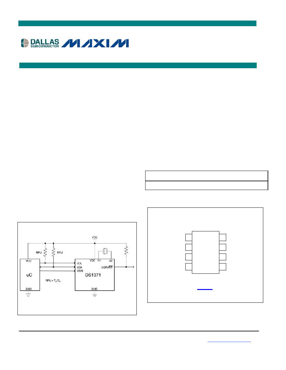
Typical Operating Circuit
Features
§ 32-Bit Binary Counter
§ 24-Bit Binary Counter Provides Periodic
Alarm, Watchdog Timer, or RAM
§ Strobe Input to Reset Watchdog Timer
§ Single Output Configurable as Interrupt or
Square Wave
§ 2-Wire Serial Interface
§ Low-Voltage Operation
§ Operating Temperature Range:
-40°C to +85°C
§ Available in 8-Pin mSOP
Ordering Information
PART TEMP
RANGE
PIN-
PACKAGE
TOP
MARK
DS1371U
-40°C to +85°C
8 µSOP
DS1371
Pin Configuration
DS1371
2-Wire, 32-Bit Binary Counter
Watchdog Clock
www.maxim-ic.com
TOP VIEW
µSOP
X1
X2
WDS
GND
1
2
3
4
8
7
6
5
V
CC
SQW/
INT
SCL
SDA
DS1371
DS1371
2 of 14
ABSOLUTE MAXIMUM RATINGS
Voltage Range on V
CC
Pin Relative to Ground
-0.3V to +6.0V
Voltage Range on SDA, SCL, and WDS Relative to Ground
-0.3V to V
CC
+0.5V
Operating Temperature Range
-40°C to +85°C
Storage Temperature Range
-55°C to +125°C
Soldering Temperature
See IPC/JEDEC J-STD-020A
Stresses beyond those listed under "Absolute Maximum Ratings" may cause permanent damage to the device. These are stress ratings only,
and functional operation of the device at these or any other conditions beyond those indicated in the operational sections of the specifications is
not implied. Exposure to absolute maximum rating conditions for extended periods can affect device reliability.
RECOMMENDED DC OPERATING CONDITIONS
(T
A
= -40°C to +85°C)
PARAMETER SYMBOL
MIN
TYP
MAX
UNITS
Supply Voltage (Note 1)
V
CC
1.7 3.3
5.5
V
Input Logic 1 (Notes 2, 3)
V
IH
0.7
V
CC
V
CC
+ 0.3
V
Input Logic 0 (Notes 2, 3)
V
IL
-0.3
0.3V
CC
V
DC ELECTRICAL CHARACTERISTICS
(V
CC
= 1.7V to 5.5V, T
A
= -40°C to +85°C, unless otherwise noted.) (Note 4)
PARAMETER SYMBOL
CONDITIONS
MIN
TYP
MAX
UNITS
Supply Voltage (Note 1)
V
CC
1.7 5.5 V
Oscillator Operating Voltage
Range (Note 1)
V
OSC
1.3 5.5 V
Input Leakage
I
LI
(Note
2)
1
mA
I/O Leakage
I
LO
(Note
3)
1
mA
V
CC
> 2V; V
OL
= 0.4V
SDA Logic 0 Output (Note 1)
I
OLSDA
V
CC
< 2V; V
OL
= 0.2V
CC
3 mA
V
CC
> 2V; V
OL
= 0.4V
3.0
1.7V < V
CC
< 2V;
V
OL
= 0.2V
CC
3.0
mA
SQW/INT Logic 0 Output
(Note 1)
I
OLSQW
1.3V < V
CC
< 1.7V;
V
OL
= 0.2V
CC
250
mA
Active Supply Current
I
CCA
(Note
5)
100 150
mA
Timekeeping Current
(Oscillator Enabled, INTCN = 1)
I
OSC0
(Notes 6, 7)
800
nA
Timekeeping Current
(Oscillator Enabled, INTCN = 0)
I
OSC1
(Notes 6, 7)
1300
nA
Data Retention Current
(Oscillator Disabled)
I
DDR
(Note
6)
50 nA
DS1371
3 of 14
AC ELECTRICAL CHARACTERISTICS
(V
CC
= 1.7V to 5.5V, T
A
= -40°C to +85°C, unless otherwise noted.) (Note 8)
PARAMETER SYMBOL
CONDITIONS
MIN
TYP
MAX
UNITS
Fast mode
100
400
SCL Clock Frequency (Note 9)
f
SCL
Standard mode
0
100
kHz
Fast mode
1.3
Bus Free Time Between STOP and
START Conditions
t
BUF
Standard mode
4.7
ms
Fast mode
0.6
Hold Time (repeated) START Condition
(Note 10)
t
HD:STA
Standard mode
4.0
ms
Fast mode
1.3
Low Period of SCL Clock
t
LOW
Standard mode
4.7
ms
Fast mode
0.6
High Period of SCL Clock
t
HIGH
Standard mode
4.0
ms
Fast mode
0
0.9
Data Hold Time (Notes 11, 12)
t
HD:DAT
Standard mode
0
0.9
ms
Fast mode
100
Data Setup Time (Note 13)
t
SU:DAT
Standard mode
250
ns
Fast mode
0.6
Start Setup Time
t
SU:STA
Standard mode
4.7
ms
Fast mode
20 +
0.1C
B
300
Rise Time of Both SDA and SCL
Signals (Note 9)
t
R
Standard mode
20 +
0.1C
B
1000
ns
Fast mode
20 +
0.1C
B
300
Fall Time of Both SDA and SCL Signals
(Note 9)
t
F
Standard mode
20 +
0.1C
B
300
ns
Fast mode
0.6
Setup Time for STOP Condition
t
SU:STO
Standard mode
4.7
ms
Capacitive Load for Each Bus Line
(Note 7)
C
B
400 pF
Pulse Width of Spikes that Must be
Suppressed by the Input Filter (Note 14)
T
SP
Fast
mode
30 ns
Watchdog Strobe (WDS) Pulse Width
t
WDS
100 ns
Oscillator Stop Flag (OSF) Delay
(Note 8)
t
OSF
100 ms
Note 1: All voltages are referenced to ground.
Note 2: SCL and WDS only.
Note 3: SDA and SQW/
INT.
Note 4: Limits at -40
°C are guaranteed by design and not production tested.
Note 5: I
CCA
--SCL clocking at max frequency = 400kHz. WDS inactive.
Note 6: Specified with WDS input and 2-wire bus inactive, SCL = SDA = V
CC
.
Note 7: Measured with a 32.768kHz crystal attached to the X1 and X2 pins.
Note 8: The parameter t
OSF
is the period of time the oscillator must be stopped in order for the OSF flag to be set over the voltage range of 1.3V
V
CC
V
CCMAX
.
Note 9: A fast mode device can be used in a standard mode system, but the requirement t
SU:DAT
to 250ns must then be met. This is
automatically the case if the device does not stretch the LOW period of the SCL signal. If such a device does stretch the LOW period of
the SCL signal, it must output the next data bit to the SDA line t
R MAX
+
t
SU:DAT
= 1000 + 250 = 1250ns before the SCL line is released.
Note 10: After this period, the first clock pulse is generated.
Note 11: A device must internally provide a hold time of at least 300ns for the SDA signal (referred to the V
IHMIN
of the SCL signal) in order to
bridge the undefined region of the falling edge of SCL.
Note 12: The maximum t
HD:DAT
has only to be met if the device does not stretch the LOW period (t
LOW
) of the SCL signal.
Note 13: C
B
--total capacitance of one bus line in pF.
Note 14: This parameter is not production tested.
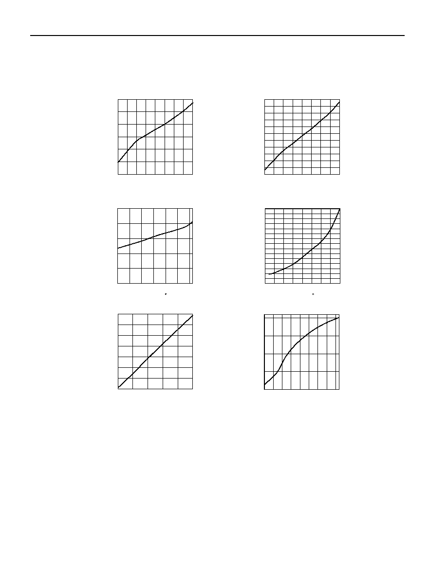
OSCILLATOR FREQUENCY vs. V
CC
DS1371 toc06
V
CC
(V)
FREQUENCY (Hz)
5.3
4.8
4.3
3.8
3.3
2.8
2.3
1.8
32767.61
32767.66
32767.71
32767.76
3.767.56
1.3
I
OSC0
vs. WDS FREQUENCY
DS1371 toc05
WDS FREQUENCY (kHz)
SUPPLY CURRENT (
µ
A)
800
600
400
200
5
10
15
20
25
30
35
0
0
1000
I
CCA
vs. V
CC
SQUARE-WAVE ON
10
15
20
25
30
35
40
45
50
55
60
65
70
75
5
0
DS1371 toc04
TEMPERATURE ( C)
SUPPLY CURRENT (
µ
A)
80
60
40
20
0
-20
-40
I
OSC0
vs. TEMPERATURE
V
CC
= 3.3V
DS1371 toc03
TEMPERATURE ( C)
SUPPLY CURRENT (nA)
80
60
40
20
0
-20
550
600
650
700
750
500
-40
I
OSC1
vs. V
CC
SQUARE-WAVE ON
DS1371 toc02
V
CC
(V)
SUPPLY CURRENT (nA)
5.0
4.5
3.5 4.0
2.5 3.0
2.0
450
500
550
600
650
700
750
800
850
900
950
400
1.5
5.5
I
OSCO
vs. V
CC
SQUARE-WAVE OFF
DS1371 toc01
V
CC
(V)
SUPPLY CURRENT (nA)
5.0
4.5
4.0
3.5
3.0
2.5
2.0
350
400
450
500
550
600
300
1.5
5.5
DS1371
4 of 14
Typical Operating Characteristics
(V
CC
= 3.3V, T
A
= +25
°C, unless otherwise noted.)
DS1371
5 of 14
Figure 1. Timing Diagram
Figure 2. Functional Diagram