General Description
The DS1374 is a 32-bit binary counter designed to contin-
uously count time in seconds. An additional counter gen-
erates a periodic alarm or serves as a watchdog timer. If
disabled, this counter can be used as 3 bytes of non-
volatile (NV) RAM. Separate output pins are provided for
an interrupt and a square wave at one of four selectable
frequencies. A precision temperature-compensated refer-
ence and comparator circuit monitor the status of V
CC
to
detect power failures, provide a reset output, and auto-
matically switch to the backup supply when necessary.
Additionally, the reset pin is monitored as a pushbutton
input for externally generating a reset. The device is pro-
grammed serially through an I
2
CTM serial interface.
Applications
Portable Instruments
Point-of-Sale Equipment
Medical Equipment
Telecommunications
Features
32-Bit Binary Counter
Second Binary Counter Provides Time-of-Day
Alarm, Watchdog Timer, or NV RAM
Separate Square-Wave and Interrupt Output Pins
I
2
C Serial Interface
Automatic Power-Fail Detect and Switch Circuitry
Single-Pin Pushbutton Reset Input/Open-Drain
Reset Output
Low-Voltage Operation
Trickle-Charge Capability
-40�C to +85�C Operating Temperature Range
10-Pin �SOP, 16-Pin SO
Available in a Surface-Mount Package with an
Integrated Crystal (DS1374C)
Underwriters Laboratory (UL) Recognized
DS1374
I
2
C, 32-Bit Binary Counter Watchdog RTC with
Trickle Charger and Reset Input/Output
______________________________________________ Maxim Integrated Products
1
Ordering Information
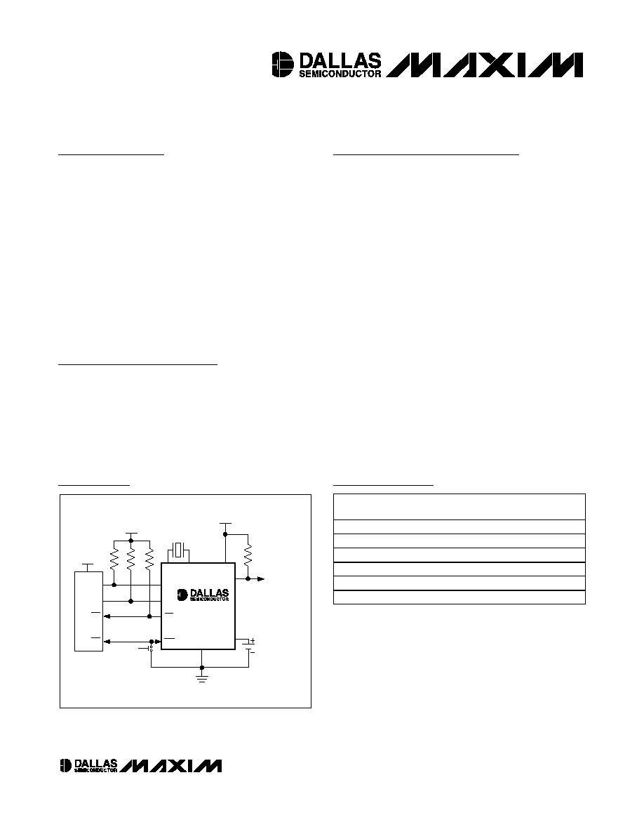
DS1374
X1
X2
CRYSTAL
V
CC
V
CC
SQW
SCL
SDA
INT
RST
INT
RST
GND
V
BACKUP
V
CC
V
CC
N.O.
PUSHBUTTON
RESET
PRIMARY
BATTERY,
RECHARGEABLE
BATTERY, OR
SUPER CAPACITOR
CPU
RPU
RPU = t
r
/C
B
RPU
Typical Operating Circuit
Rev 1; 9/04
For pricing, delivery, and ordering information, please contact Maxim/Dallas Direct! at
1-888-629-4642, or visit Maxim's website at www.maxim-ic.com.
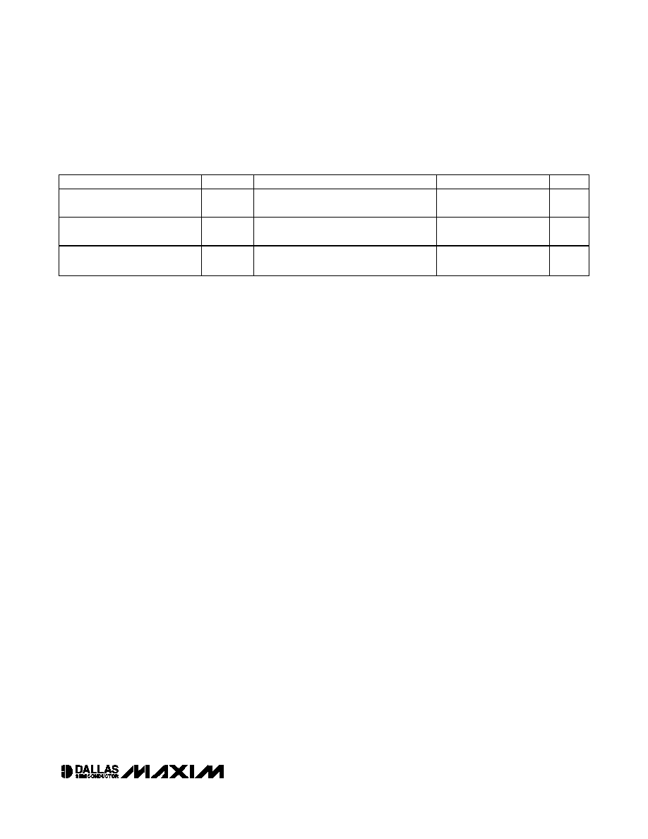
PART
TEMP RANGE
PIN-
PACKAGE
TOP MARK
DS1374U-18
-40�C to +85�C 10 �SOP
DS1374-18
DS1374U-3
-40�C to +85�C 10 �SOP
DS1374-3
DS1374U-33
-40�C to +85�C 10 �SOP
DS1374-33
DS1374C-18
-40�C to +85�C 16 SO, 0.300"
DS1374C-18
DS1374C-3
-40�C to +85�C 16 SO, 0.300"
DS1374C-3
DS1374C-33
-40�C to +85�C 16 SO, 0.300"
DS1374C-33
I
2
C is a trademark of Philips Corp. Purchase of I
2
C compo-
nents of Maxim Integrated Products, Inc., or one of its subli-
censed Associated Companies, conveys a license under the
Philips I
2
C Patent Rights to use these components in an I
2
C
system, provided that the system conforms to the I
2
C Standard
Specification as defined by Philips.
Pin Configurations appear at the end of the data sheet.
DS1374
I
2
C, 32-Bit Binary Counter Watchdog RTC with
Trickle Charger and Reset Input/Output
2
_____________________________________________________________________
ABSOLUTE MAXIMUM RATINGS
RECOMMENDED DC OPERATING CONDITIONS
(V
CC
= V
CC MIN
to V
CC MAX
, T
A
= -40�C to +85�C, unless otherwise noted.) (Note 1)
Stresses beyond those listed under "Absolute Maximum Ratings" may cause permanent damage to the device. These are stress ratings only, and functional
operation of the device at these or any other conditions beyond those indicated in the operational sections of the specifications is not implied. Exposure to
absolute maximum rating conditions for extended periods may affect device reliability.
Voltage Range on V
CC
Pin Relative to Ground .....-0.3V to +6.0V
Voltage Range on SDA, SCL, and WDS
Relative to Ground ....................................-0.3V to V
CC
+ 0.3V
Operating Temperature Range ...........................-40
�C to +85�C
Storage Temperature Range .............................-55
�C to +125�C
Soldering Temperature Range ........................See the Handling,
PC Board Layout, and Assembly section.
PARAMETER
SYMBOL
CONDITIONS
MIN
TYP
MAX
UNITS
DS1374-33
2.97
3.3
5.50
DS1374-3
2.7
3.0
3.3
Supply Voltage
(Notes 2, 3)
V
CC
DS1374-18
1.71
1.8
1.89
V
Input Logic 1
V
IH
(Note 2)
0.7 x V
CC
V
CC
+ 0.3
V
Input Logic 0
V
IL
(Note 2)
-0.3
+0.3 x
V
CC
V
Pullup Resistor Voltage (
INT,
SQW, SDA, SCL), V
CC
= 0V
V
PU
(Note 2)
5.5
V
DS1374-33
2.70
2.88
2.97
DS1374-3
2.45
2.6
2.7
Power-Fail Voltage
(Note 2)
V
PF
DS1374-18
1.51
1.6
1.71
V
DS1374-33
1.3
3.0
V
CC
MAX
DS1374-3
1.3
3.0
3.7
Backup Supply Voltage
(Notes 2, 3, 4)
V
BACKUP
V
DS1374
I
2
C, 32-Bit Binary Counter Watchdog RTC with
Trickle Charger and Reset Input/Output
_____________________________________________________________________
3
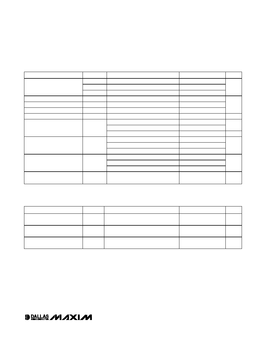
DC ELECTRICAL CHARACTERISTICS
(V
CC
= V
CC MIN
to V
CC MAX
, T
A
= -40�C to +85�C, unless otherwise noted.) (Note 1)
PARAMETER
SYMBOL
CONDITIONS
MIN
TYP
MAX
UNITS
R1
(Note 5)
250
R2
(Note 6)
2000
Trickle-Charge Current-Limiting
Resistors
R3
(Note 7)
4000
Input Leakage
I
LI
(Note 8)
-1
+1
I/O Leakage
I
LO
(Note 9)
-1
+1
RST Pin I/O Leakage
I
LORST
(Note 10)
-200
+1
�A
SDA Logic 0 Output (V
OL
= 0.4V)
I
OLSDA
3.0
mA
V
CC
> 2V; V
OL
= 0.4V
3.0
1.71V < V
CC
< 2V; V
OL
= 0.2 V
CC
3.0
mA
RST, SQW, and INT Logic 0
Outputs (Note 11)
I
OL1
1.3V < V
CC
< 1.71V; V
OL
= 0.2 V
CC
250
�A
DS1374-18
75
150
DS1374-3
110
200
Active Supply Current
(Notes 11, 12)
I
CCA
DS1374-33
180
300
�A
DS1374-18
60
100
DS1374-3
80
125
Standby Current (Notes 11, 13)
I
CCS
DS1374-33
115
175
�A
V
BACKUP
Leakage Current
(V
BACKUP
= 3.7V)
I
BACKUPLKG
100
nA
DC ELECTRICAL CHARACTERISTICS
(V
CC
= 0V, V
BACKUP
= 3.7V, T
A
= -40�C to +85�C, unless otherwise noted.) (Note 1)
PARAMETER
SYMBOL
CONDITIONS
MAX
TYP
MAX
UNITS
V
BACKUP
Current (OSC ON);
SQW OFF
I
BKOSC1
(Note 14)
400
700
nA
V
BACKUP
Current (OSC ON);
SQW ON (32kHz)
I
BKOSC2
(Notes 14, 15)
600
1000
nA
V
BACKUP
Data-Retention Current
(OSC OFF)
I
BACKUPDR
25
100
nA
DS1374
I
2
C, 32-Bit Binary Counter Watchdog RTC with
Trickle Charger and Reset Input/Output
4
_____________________________________________________________________
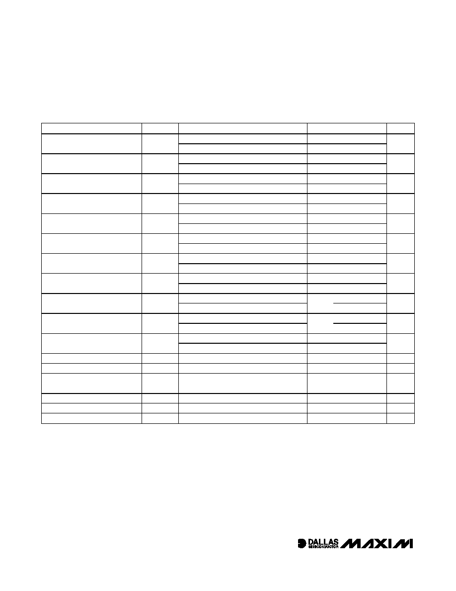
AC ELECTRICAL CHARACTERISTICS
(V
CC
= V
CC MIN
to V
CC MAX
, T
A
= -40�C to +85�C, unless otherwise noted.) (Note 1) (Figure 1)
PARAMETER
SYMBOL
CONDITIONS
MIN
TYP
MAX
UNITS
Fast mode
100
400
SCL Clock Frequency (Note 16)
f
SCL
Standard mode
0
100
kHz
Fast mode
1.3
Bus Free Time Between STOP
and START Conditions
t
BUF
Standard mode
4.7
�s
Fast mode
0.6
Hold Time (Repeated) START
Condition (Note 17)
t
HD:STA
Standard mode
4.0
�s
Fast mode
1.3
Low Period of SCL Clock
t
LOW
Standard mode
4.7
�s
Fast mode
0.6
High Period of SCL Clock
t
HIGH
Standard mode
4.0
�s
Fast mode
0
0.9
Data Hold Time (Notes 18, 19)
t
HD:DAT
Standard mode
0
0.9
�s
Fast mode
100
Data Setup Time (Note 20)
t
SU:DAT
Standard mode
250
ns
Fast mode
0.6
Start Setup Time
t
SU:STA
Standard mode
4.7
�s
Fast mode
300
Rise Time of Both SDA and SCL
Signals (Note 16)
t
R
Standard mode
20 +
0.1C
B
1000
ns
Fast mode
300
Fall Time of Both SDA and SCL
Signals (Note 16)
t
F
Standard mode
20 +
0.1C
B
300
ns
Fast mode
0.6
Setup Time for STOP Condition
t
SU:STO
Standard mode
4.7
�s
C ap aci ti ve Load for E ach Bus Li ne
C
B
(Note 16)
400
pF
I/O C ap aci tance ( S D A, S C L) C
I/O
(Note 21)
10
pF
Pulse Width of Spikes That Must
be Suppressed by the Input Filter
t
SP
Fast mode
30
ns
Pushbutton Debounce
PB
DB
(Figure 2)
250
ms
Reset Active Time
t
RST
(Figure 2)
250
ms
Oscillator Stop Flag (OSF) Delay
t
OSF
(Note 22)
100
ms
DS1374
I
2
C, 32-Bit Binary Counter Watchdog RTC with
Trickle Charger and Reset Input/Output
_____________________________________________________________________
5
POWER-UP/POWER-DOWN CHARACTERISTICS
(T
A
= -40�C to +85�C) (Figure 3)
PARAMETER
SYMBOL
CONDITIONS
MIN
TYP
MAX
UNITS
V
CC
Detect to Recognize Inputs
(V
CC
Rising)
t
RPU
(Note 23)
250
ms
V
CC
Fall Time; V
PF(MAX)
to
V
PF(MIN)
t
F
300
�s
V
CC
Rise Time; V
PF(MIN)
to
V
PF(MAX)
t
R
0
�s
WARNING: Under no circumstances are negative undershoots, of any amplitude, allowed when the device is in write protection.
Note 1:
Limits at -40�C are guaranteed by design and not production tested.
Note 2:
All voltages are referenced to ground.
Note 3:
V
BACKUP
should not exceed V
CC
MAX or 3.7V, whichever is greater.
Note 4:
The use of the 250
trickle-charge resistor is not allowed at V
CC
> 3.63V and should not be enabled.
Note 5:
Measured at V
CC
= typ, V
BACKUP
= 0V, register 09h = A5h.
Note 6:
Measured at V
CC
= typ, V
BACKUP
= 0V, register 09h = A6h.
Note 7:
Measured at V
CC
= typ, V
BACKUP
= 0V, register 09h = A7h.
Note 8:
SCL only.
Note 9:
SDA and SQW and
INT.
Note 10: The
RST pin has an internal 50k
pullup resistor to V
CC
.
Note 11: Trickle charger disabled.
Note 12: I
CCA
--SCL clocking at max frequency = 400kHz.
Note 13: Specified with I
2
C bus inactive.
Note 14: Measured with a 32.768kHz crystal attached to the X1 and X2 pins.
Note 15: WDSTR = 1. BBSQW = 1 is required for operation when V
CC
is below the power-fail trip point (or absent).
Note 16: C
B
--total capacitance of one bus line in pF.
Note 17: After this period, the first clock pulse is generated.
Note 18: The maximum t
HD:DAT
only has to be met if the device does not stretch the low period (t
LOW
) of the SCL signal.
Note 19: A device must internally provide a hold time of at least 300ns for the SDA signal (referred to as the V
IHMIN
of the SCL sig-
nal) to bridge the undefined region of the falling edge of SCL.
Note 20: A fast-mode device can be used in a standard-mode system, but the requirement t
SU:DAT
to 250ns must be met. This is
automatically the case if the device does not stretch the low period of the SCL signal. If such a device does stretch the low
period of the SCL signal, it must output the next data bit to the SDA line t
R
max + t
SU:DAT
= 1000 + 250 = 1250ns before
the SCL line is released.
Note 21: Guaranteed by design. Not production tested.
Note 22: The parameter t
OSF
is the period of time the oscillator must be stopped for the OSF flag to be set over the voltage range of
0V
V
CC
V
CC MAX
and 1.3V
V
BACKUP
3.7V.
Note 23: This delay applies only if the oscillator is enabled and running. If the
EOSC bit is 1, the startup time of the oscillator is
added to this delay.