 | –≠–ª–µ–∫—Ç—Ä–æ–Ω–Ω—ã–π –∫–æ–º–ø–æ–Ω–µ–Ω—Ç: DS1388Z-5 | –°–∫–∞—á–∞—Ç—å:  PDF PDF  ZIP ZIP |

General Description
The DS1388 I
2
C real-time clock (RTC), supervisor, and
EEPROM is a multifunction device that provides a
clock/calendar, programmable watchdog timer, power-
supply monitor with reset, and 512 bytes of EEPROM.
The clock provides hundredths of seconds, seconds,
minutes, and hours, and operates in 24-hour or 12-hour
format with an AM/PM indicator. The calendar provides
day, date, month, and year information. The date at the
end of the month is automatically adjusted for months
with fewer than 31 days, including corrections for leap
year. A watchdog timer provides a reset for an unre-
sponsive microprocessor. It is programmable in 10ms
intervals from 0.01 to 99.99 seconds. A temperature-
compensated voltage reference and comparator circuit
monitors the status of V
CC
. If a primary power failure is
detected, the device automatically switches to the
backup supply and drives the reset output to the active
state. The backup supply maintains time and date
operation in the absence of V
CC
. When V
CC
returns to
nominal levels, the reset is held low for a period to allow
the power supply and processor to stabilize. The
device also has a pushbutton reset controller, which
debounces a reset input signal. The device is
accessed through an I
2
C serial interface.
Applications
Portable Instruments
Point-of-Sale Equipment
Network Interface Cards
Wireless Equipment
Features
Fast (400kHz) I
2
C Interface
RTC Counts Hundredths of Seconds, Seconds,
Minutes, Hours, Day, Date, Month, and Year with
Leap Year Compensation Valid Up to 2100
Programmable Watchdog Timer
Automatic Power-Fail Detect and Switch Circuitry
Reset Output with Pushbutton Reset Input
Capability
512 x 8 Bits of EEPROM
Integrated Trickle-Charge Capability for Backup
Supply
Three Operating Voltages: 5.0V, 3.3V, and 3.0V
Low Timekeeping Voltage Down to 1.3V
-40∞C to +85∞C Temperature Range
UL Recognized
DS1388
I
2
C RTC/Supervisor with Trickle Charger
and 512 Bytes EEPROM
______________________________________________ Maxim Integrated Products
1
1
2
3
4
8
7
6
5
V
CC
RST
SCL
SDA
V
BACKUP
GND
X2
X1
TOP VIEW
DS1388
SO
Pin Configuration
RST
V
CC
X1
SCL
X2
CPU
V
CC
DS1388
SDA
GND
V
CC
RPU
RPU = t
r
/C
B
RPU
V
CC
CRYSTAL
V
BACKUP
Typical Operating Circuit
Rev 0; 4/05
For pricing, delivery, and ordering information, please contact Maxim/Dallas Direct! at
1-888-629-4642, or visit Maxim's website at www.maxim-ic.com.
A '+' symbol near the pin one indicator indicates lead-free.
+ = Lead free.
Ordering Information
PART
TEMP RANGE
PIN-
PACKAGE
TOP
MARK
DS1388Z-3
-40∞C to +85∞C 8 SO (150 mils)
DS1388-3
DS1388Z-33
-40∞C to +85∞C 8 SO (150 mils)
DS138833
DS1388Z-5
-40∞C to +85∞C 8 SO (150 mils)
DS1388-5
DS1388Z-5+
-40∞C to +85∞C 8 SO (150 mils)
DS1388-5
DS1388Z-33+
-40∞C to +85∞C 8 SO (150 mils)
DS138833
DS1388Z-3+
-40∞C to +85∞C 8 SO (150 mils)
DS1388-3
Purchase of I
2
C components from Maxim Integrated Products,
Inc., or one of its sublicensed Associated Companies, conveys
a license under the Philips I
2
C Patent Rights to use these com-
ponents in an I
2
C system, provided that the system conforms
to the I
2
C Standard Specification as defined by Philips.
DS1388
I
2
C RTC/Supervisor with Trickle Charger
and 512 Bytes EEPROM
2
_____________________________________________________________________
ABSOLUTE MAXIMUM RATINGS
RECOMMENDED DC OPERATING CONDITIONS
(T
A
= -40∞C to +85∞C, unless otherwise noted.) (Note 1)
Stresses beyond those listed under "Absolute Maximum Ratings" may cause permanent damage to the device. These are stress ratings only, and functional
operation of the device at these or any other conditions beyond those indicated in the operational sections of the specifications is not implied. Exposure to
absolute maximum rating conditions for extended periods may affect device reliability.
Voltage Range on V
CC
Pin Relative to Ground .....-0.3V to +6.0V
Voltage Range on Inputs Relative
to Ground ...............................................-0.3V to (V
CC
+ 0.3V)
Operating Temperature Range
(noncondensing) .............................................-40∞C to +85∞C
Storage Temperature Range .............................-55∞C to +125∞C
Soldering Temperature .....................See IPC/JEDEC J-STD-020
Specification
PARAMETER
SYMBOL
CONDITIONS
MIN
TYP
MAX
UNITS
DS1388Z-5
4.5
5
5.5
DS1388Z-33
2.97
3.3
3.63
Supply Voltage
V
CC
(Note 2)
DS1388Z-3
2.7
3
3.3
V
Logic 1
V
IH
(Note 2)
0.7 x
V
CC
V
CC
+
0.3
V
Logic 0
V
IL
(Note 2)
-0.3
+0.3 x
V
CC
V
Pullup Voltage (SCL, SDA),
V
CC
= 0V
V
PU
5.5
V
V
BACKUP
Voltage
V
BACKUP
(Note 2)
1.3
3.0
5.5
V
DS1388Z-5
4.15
4.33
4.50
DS1388Z-33
2.70
2.88
2.97
Power-Fail Voltage
V
PF
(Note 2)
DS1388Z-3
2.45
2.60
2.70
V
DC ELECTRICAL CHARACTERISTICS
(V
CC
= V
CC(MIN)
to V
CC(MAX)
, T
A
= -40∞C to +85∞C, unless otherwise noted.) (Note 1)
PARAMETER
SYMBOL
CONDITIONS
MIN
TYP
MAX
UNITS
R1
(Notes 3, 4)
250
R2
(Note 5)
2000
Trickle-Charger Current-Limiting
Resistors
R3
(Note 6)
4000
Input Leakage (SCL)
I
LI
-1
+1
µA
I/O Leakage (SDA)
I
LO
-1
+1
µA
I/O Leakage (RST)
I
LORST
(Note 7)
-200
+10
µA
SDA Logic 0 Output
(V
OL
= 0.15 x V
CC
)
I
OLDOUT
3
mA

DS1388
I
2
C RTC/Supervisor with Trickle Charger
and 512 Bytes EEPROM
_____________________________________________________________________
3
DC ELECTRICAL CHARACTERISTICS (continued)
(V
CC
= V
CC(MIN)
to V
CC(MAX)
, T
A
= -40∞C to +85∞C, unless otherwise noted.) (Note 1)
PARAMETER
SYMBOL
CONDITIONS
MIN
TYP
MAX
UNITS
V
CC
> 2V; V
OL
= 0.4V
3.0
1.8V < V
CC
< 2V; V
OL
= 0.2 x V
CC
3.0
mA
RST Logic 0 Output
I
OLSIR
1.3V < V
CC
< 1.8V; V
OL
= 0.2 x V
CC
250
µA
DS1388Z-5
600
DS1388Z-33
250
V
CC
Active Current, EEPROM
Read, I
2
C Read/Write Access
I
CCER
(Note 8)
DS1388Z-3
225
µA
DS1388Z-5
1.0
DS1388Z-33
0.70
V
CC
Active Current, EEPROM
Write Cycle
I
CCEW
(Note 8)
DS1388Z-3
0.65
mA
DS1388Z-5
270
DS1388Z-33
100
150
V
CC
Standby Current
I
CCS
(Note 9)
DS1388Z-3
140
µA
V
BACKUP
Leakage Current
(V
BACKUP
= 3.7V,
V
CC
= V
CC(MAX)
)
I
BACKUPLKG
15
100
nA
T
A
= +25∞C (guaranteed by design)
200k
EEPROM Write/Erase Cycles
t
WR
T
A
= -40∞C to +85∞C (guaranteed by
design)
50k
Cycles
DC ELECTRICAL CHARACTERISTICS
(V
CC
= 0V, V
BACKUP
= 3.7V, T
A
= +25∞C, unless otherwise noted.) (Note 1)
PARAMETER
SYMBOL
CONDITIONS
MIN
TYP
MAX
UNITS
V
BACKUP
Current, OSC On
(EOSC = 0), SDA = SCL = 0V
I
BACKUP
(Note 10)
410
550
nA
V
BACKUP
Current, OSC Off
(EOSC = 1), SDA = SCL = 0V
(Data Retention)
I
BACKUPDR
(Note 10)
10
100
nA

DS1388
I
2
C RTC/Supervisor with Trickle Charger
and 512 Bytes EEPROM
4
_____________________________________________________________________
AC ELECTRICAL CHARACTERISTICS
(V
CC
= V
CC(MIN)
to V
CC(MAX)
, T
A
= -40∞C to +85∞C, unless otherwise noted.) (Note 1)
PARAMETER
SYMBOL
CONDITION
MIN
TYP
MAX
UNITS
Fast mode
100
400
SCL Clock Frequency
f
SCL
Standard mode
0
100
kHz
Fast mode
1.3
Bus Free Time Between a STOP
and START Condition
t
BUF
Standard mode
4.7
µs
Fast mode
0.6
Hold Time (Repeated) START
Condition (Note 11)
t
HD:STA
Standard mode
4.0
µs
Fast mode
1.3
LOW Period of SCL Clock
t
LOW
Standard mode
4.7
µs
Fast mode
0.6
HIGH Period of SCL Clock
t
HIGH
Standard mode
4.0
µs
Fast mode
0.6
Setup Time for a Repeated
START Condition
t
SU:STA
Standard mode
4.7
µs
Fast mode
0
0.9
Data Hold Time (Notes 12, 13)
t
HD:DAT
Standard mode
0
µs
Fast mode
100
Data Setup Time (Note 14)
t
SU:DAT
Standard mode
250
ns
Fast mode
300
Rise Time of Both SDA and SCL
Signals (Note 15)
t
R
Standard mode
20 +
0.1C
B
1000
ns
Fast mode
300
Fall Time of Both SDA and SCL
Signals (Note 15)
t
F
Standard mode
20 +
0.1C
B
300
ns
Fast mode
0.6
Setup Time for STOP Condition
t
SU:STO
Standard mode
4.0
µs
Capacitive Load for Each Bus
Line (Note 15)
C
B
400
pF
I/O Capacitance (SDA, SCL, RST)
C
I/O
+25∞C
10
pF
Pushbutton Debounce
PB
DB
160
180
ms
Reset Active Time
t
RST
160
180
ms
EEPROM Write Cycle Time
t
WEE
8
10
ms
Oscillator Stop Flag (OSF) Delay
(Note 16)
t
OSF
20
ms
DS1388
I
2
C RTC/Supervisor with Trickle Charger
and 512 Bytes EEPROM
_____________________________________________________________________
5
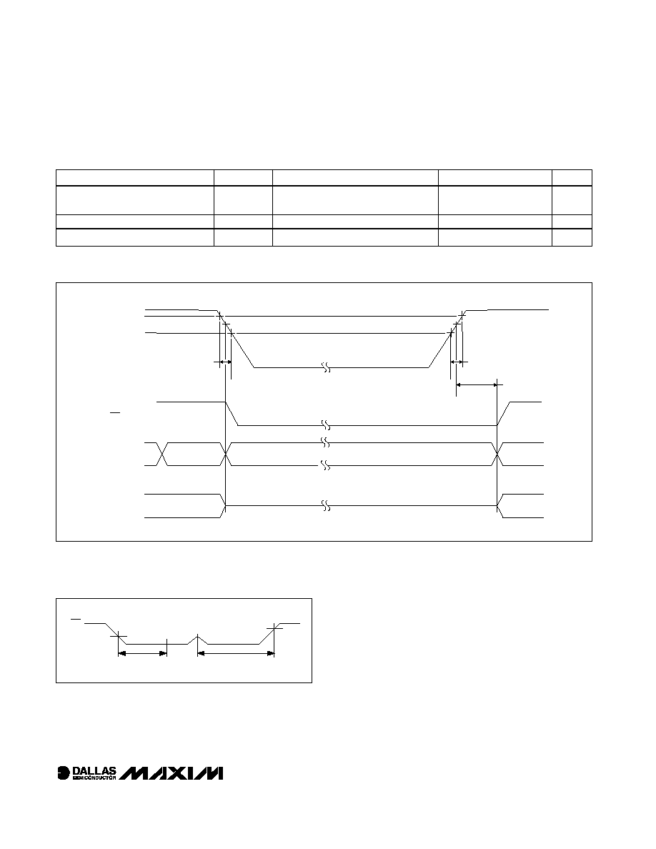
POWER-UP/POWER-DOWN CHARACTERISTICS
(T
A
= -40∞C to +85∞C) (Note 1) (Figures 1, 2)
PARAMETER
SYMBOL
CONDITIONS
MIN
TYP
MAX
UNITS
V
CC
Detect to Recognize Inputs
(V
CC
Rising)
t
RST
(Note 17)
160
180
ms
V
CC
Fall Time; V
PF(MAX)
to V
PF(MIN)
t
F
300
µs
V
CC
Rise Time; V
PF(MIN)
to V
PF(MAX)
t
R
0
µs
OUTPUTS
V
CC
V
PF(MAX)
INPUTS
HIGH IMPEDANCE
RST
DON'T CARE
VALID
RECOGNIZED
RECOGNIZED
VALID
V
PF(MIN)
tRST
tRPU
tR
tF
V
PF
V
PF
Figure 1. Power-Up/Down Timing
t
RST
PB
DB
RST
Figure 2. Pushbutton Reset Timing