General Description
The low-voltage serial-peripheral interface (SPITM)
DS1390/DS1391 and the low-voltage 3-wire DS1392/
DS1393 real-time clocks (RTCs) are clocks/calendars
that provide hundredths of a second, seconds, min-
utes, hours, day, date, month, and year information.
The date at the end of the month is automatically
adjusted for months with fewer than 31 days, including
corrections for leap year. The clock operates in either
the 24-hour or 12-hour format with an AM/PM indicator.
One programmable time-of-day alarm is provided. A
temperature-compensated voltage reference monitors
the status of V
CC
and automatically switches to the
backup supply if a power failure is detected. On the
DS1390, a single open-drain output provides a CPU
interrupt or a square wave at one of four selectable fre-
quencies. The DS1391 replaces the SQW/INT pin with a
RST output/debounced input.
The DS1390 and DS1391 are programmed serially
through an SPI-compatible, bidirectional bus. The
DS1392 and DS1393 communicate over a 3-wire serial
bus, and the extra pin is used for either a separate
interrupt pin or a RST output/debounced input.
All four devices are available in a 10-pin µSOP package,
and are rated over the industrial temperature range.
Applications
Hand-Held Devices
GPS/Telematics Devices
Embedded Time Stamping
Medical Devices
Features
Real-Time Clock Counts Hundredths of Seconds,
Seconds, Minutes, Hours, Day, Date, Month, and
Year with Leap-Year Compensation Valid Up to
2100
Output Pin Configurable as Interrupt or Square
Wave with Programmable Frequency of
32.768kHz, 8.192kHz, 4.096kHz, or 1Hz
(DS1390/DS1393 Only)
One Time-of-Day Alarm
Power-Fail Detect and Switch Circuitry
Reset Output/Debounced Input (DS1391/DS1393)
Separate SQW and INT Output (DS1392)
Trickle-Charge Capability
SPI Supports Modes 1 and 3 (DS1390/DS1391)
3-Wire Interface (DS1392/DS1393)
4MHz at 3.0V and 3.3V
1MHz at 1.8V
Three Operating Voltages: 1.8V ±5%, 3.0V ±10%,
and 2.97 to 5.5V
Industrial Temperature Range: -40∞C to +85∞C
Underwriters Laboratory (UL) Recognized
DS1390/DS1391/DS1392/DS1393
Low-Voltage SPI/3-Wire RTCs with
Trickle Charger
______________________________________________ Maxim Integrated Products
1
Ordering Information
Rev 0; 7/04
For pricing, delivery, and ordering information, please contact Maxim/Dallas Direct! at
1-888-629-4642, or visit Maxim's website at www.maxim-ic.com.
Typical Operating Circuits and Pin Configurations appear at
end of the data sheet.
Where "rr" is a revision code on the second line of the top mark.
PART
TEMP RANGE
PIN-
PACKAGE
TOP MARK
DS1390U-18
-40∞C to +85∞C
10 µSOP
DS1390 rr-18
DS1390U-3
-40∞C to +85∞C
10 µSOP
DS1390 rr-3
DS1390U-33
-40∞C to +85∞C
10 µSOP
DS1390 rr-33
DS1391U-18
-40∞C to +85∞C
10 µSOP
DS1391 rr-18
DS1391U-3
-40∞C to +85∞C
10 µSOP
DS1391 rr-3
DS1391U-33
-40∞C to +85∞C
10 µSOP
DS1391 rr-33
DS1392U-18
-40∞C to +85∞C
10 µSOP
DS1393 rr-18
DS1392U-3
-40∞C to +85∞C
10 µSOP
DS1392 rr-3
DS1392U-33
-40∞C to +85∞C
10 µSOP
DS1392 rr-33
DS1393U-18
-40∞C to +85∞C
10 µSOP
DS1393 rr-18
DS1393U-3
-40∞C to +85∞C
10 µSOP
DS1393 rr-3
DS1393U-33
-40∞C to +85∞C
10 µSOP
DS1393 rr-33
SPI is a trademark of Motorola, Inc.
DS1390/DS1391/DS1392/DS1393
Low-Voltage SPI/3-Wire RTCs with
Trickle Charger
2
_____________________________________________________________________
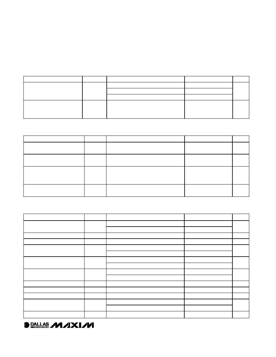
ABSOLUTE MAXIMUM RATINGS
RECOMMENDED DC OPERATING CONDITIONS
(V
CC
= V
CC(MIN)
to V
CC(MAX)
, T
A
= -40∞C to +85∞C, unless otherwise noted. Typical values are at nominal supply voltage and T
A
= +25∞C,
unless otherwise noted.) (Note 1)
Stresses beyond those listed under "Absolute Maximum Ratings" may cause permanent damage to the device. These are stress ratings only, and functional
operation of the device at these or any other conditions beyond those indicated in the operational sections of the specifications is not implied. Exposure to
absolute maximum rating conditions for extended periods may affect device reliability.
Voltage Range on V
CC
Pin Relative to Ground .....-0.3V to +6.0V
Voltage Range on Inputs Relative
to Ground ...............................................-0.3V to (V
CC
+ 0.3V)
Operating Temperature Range ...........................-40
∞C to +85∞C
Storage Temperature Range .............................-55∞C to +125∞C
Soldering Temperature .......................................See IPC/JEDEC
J-STD-020A Specification
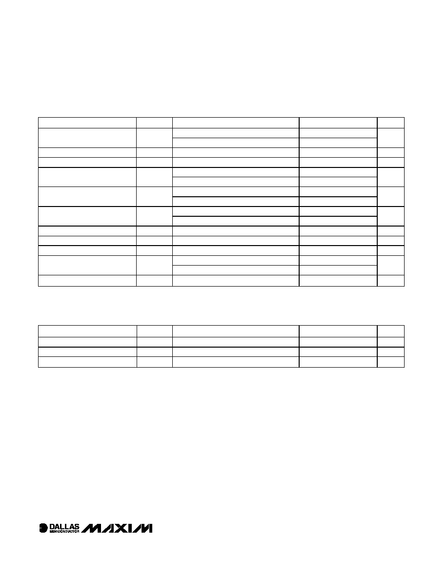
PARAMETER
SYMBOL
CONDITIONS
MIN
TYP
MAX
UNITS
DS139x-33
2.97
3.3
5.50
DS139x-3
2.7
3.0
3.3
Supply Voltage (Note 2)
V
CC
DS139x-18
1.71
1.8
1.89
V
Logic 1
V
IH
(Note 2)
0.7 x
V
CC
V
CC
+
0.5
V
Logic 0
V
IL
(Note 2)
-0.3
+0.3 x
V
CC
V
Supply Voltage, Pullup
SQW/INT, SQW, INT, V
CC
= 0V
V
PU
(Note 2)
5.5
V
-33
1.3
3.0
V
CC(MAX)
-3
1.3
3.0
3.7
V
BACKUP
Voltage (Note 2)
V
BACKUP
-18
1.3
3.0
3.7
V
-33
2.70
2.88
2.97
-3
2.45
2.6
2.70
Power-Fail Voltage (Note 2)
V
PF
-18
1.51
1.6
1.71
V
R1
(Notes 3, 4)
250
R2
(Notes 3, 5)
2000
Trickle-Charge Current-Limiting
Resistors
R3
(Notes 3, 6)
4000
Input Leakage
I
LI
(Note 7)
-1
+1
µA
I/O Leakage
I
LO
(Note 8)
-1
+1
µA
RST Pin I/O Leakage
I
LORST
(Note 9)
-200
+10
µA
-33, -3 (V
OH
= 0.85 x V
CC
)
-1
DOUT Logic 1 Output
I
OHDOUT
-18 (V
OH
= 0.80 x V
CC
)
0.750
mA
-33, -3 (V
OL
= 0.15 x V
CC
)
3
DOUT Logic 0 Output
I
OHDOUT
-18 (V
OL
= 0.20 x V
CC
)
2
mA
V
CC
> 1.71V; V
OL
= 0.4V
3.0
mA
Logic 0 Output
(DS1390/DS1393 SQW/INT;
DS1392 SQW, INT;
DS1391/DS1393 RST)
I
OLSIR
1.3V < V
CC
< 1.71V; V
OL
= 0.4V
250
µA
-33
2
-3
2
mA
V
CC
Active Supply Current
(Note 10)
I
CCA
-18
500
µA
DS1390/DS1391/DS1392/DS1393
Low-Voltage SPI/3-Wire RTCs with
Trickle Charger
_____________________________________________________________________
3
RECOMMENDED DC OPERATING CONDITIONS (continued)
(V
CC
= V
CC(MIN)
to V
CC(MAX)
, T
A
= -40∞C to +85∞C, unless otherwise noted. Typical values are at nominal supply voltage and T
A
= +25∞C,
unless otherwise noted.) (Note 1)
PARAMETER
SYMBOL
CONDITIONS
MIN
TYP
MAX
UNITS
-33
115
175
-3
80
125
V
CC
Standby Current
(Note 11)
I
CCS
-18
60
100
µA
V
BACKUP
Leakage Current
(V
BACKUP
= 3.7V,
V
CC
= V
CC(MAX)
)
I
BACKUPLKG
15
100
nA
DC ELECTRICAL CHARACTERISTICS
(V
CC
= 0V, V
BACKUP
= 3.7V, T
A
= -40∞C to +85∞C, unless otherwise noted.) (Note 1)
PARAMETER
SYMBOL
CONDITIONS
MIN
TYP
MAX
UNITS
V
BACKUP
Current OSC On,
SQW Off
I
BACKUP1
(Note 12)
500
1000
nA
V
BACKUP
Current OSC On,
SQW On (32kHz)
I
BACKUP2
(Note 12)
600
1150
nA
V
BACKUP
Current OSC On,
SQW On, V
BACKUP
= 3.0V,
T
A
= +25∞C
I
BACKUP3
(Note 12)
600
1000
nA
V
BACKUP
Current, OSC Off
(Data Retention)
I
BACKUPDR
(Note 12)
25
100
nA
AC ELECTRICAL CHARACTERISTICS--SPI INTERFACE
(V
CC
= V
CC(MIN)
to V
CC(MAX)
, T
A
= -40∞C to +85∞C, unless otherwise noted.) (Note 1)
PARAMETER
SYMBOL
CONDITION
MIN
TYP
MAX
UNITS
2.7V
V
CC
5.5V
4
SCLK Frequency (Note 13)
f
SCLK
1.71V
V
CC
1.89V
1
MHz
Data to SCLK Setup
t
DC
(Notes 13, 14)
30
ns
SCLK to Data Hold
t
CDH
(Notes 13, 14)
30
ns
2.7V
V
CC
5.5V
80
SCLK to Data Valid
(Notes 13, 14, 15)
t
CDD
1.71V
V
CC
1.89V
160
ns
2.7V
V
CC
. 5.5V
110
SCLK Low Time (Note 13)
t
CL
1.71V
V
CC
1.89V
400
ns
2.7V
V
CC
5.5V
110
SCLK High Time (Note 13)
t
CH
1.71V
V
CC
1.89V
400
ns
SCLK Rise and Fall
t
R
, t
F
200
ns
CS to SCLK Setup (Note 13)
t
CC
400
ns
SCLK to CS Hold (Note 13)
t
CCH
100
ns
2.7V
V
CC
. 5.5V
400
CS Inactive Time (Note 13)
t
CWH
1.71V
V
CC
1.89V
500
ns
CS to Output High Impedance
t
CDZ
(Notes 13, 14)
40
ns
DS1390/DS1391/DS1392/DS1393
Low-Voltage SPI/3-Wire RTCs with
Trickle Charger
4
_____________________________________________________________________
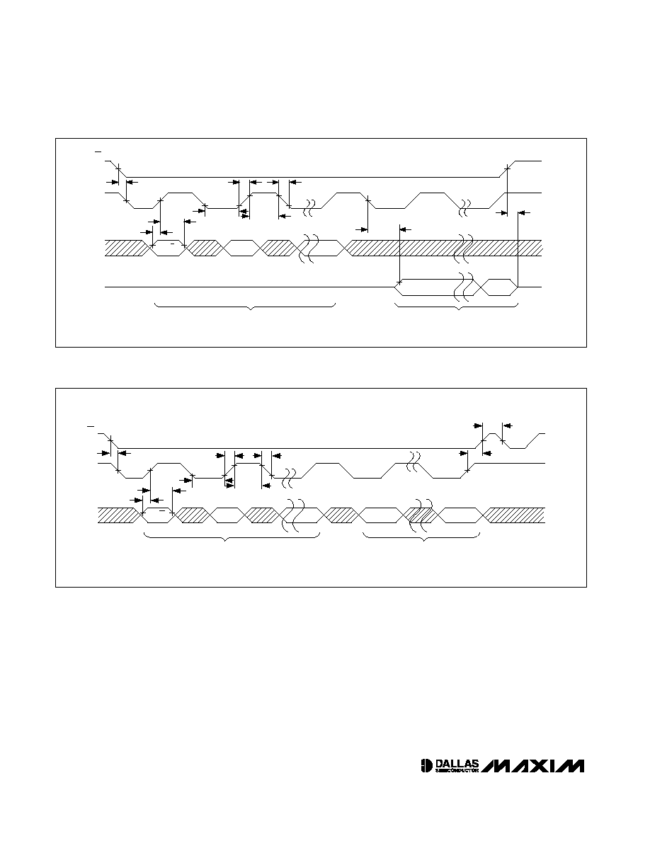
CS
SCLK
DIN
W/R
t
DC
t
CL
t
CH
t
CDD
t
CDZ
t
CDH
t
CC
t
R
t
F
A6
A0
D0
WRITE ADDRESS BYTE
NOTE: SCLK CAN BE EITHER POLARITY, SHOWN FOR CPOL = 1.
READ DATA BYTE
DOUT
D7
Figure 1. Timing Diagram--SPI Read Transfer
CS
SCLK
DIN
W/R
t
DC
t
CDH
t
CL
t
CH
t
CCH
t
CWH
t
F
t
R
t
CC
A6
A0
WRITE ADDRESS BYTE
WRITE DATA BYTE
D7
D0
Figure 2. Timing Diagram--SPI Write Transfer
DS1390/DS1391/DS1392/DS1393
Low-Voltage SPI/3-Wire RTCs with
Trickle Charger
_____________________________________________________________________
5
AC ELECTRICAL CHARACTERISTICS--3-WIRE INTERFACE
(V
CC
= V
CC(MIN)
to V
CC(MAX)
, T
A
= -40∞C to +85∞C.) (Note 1) (Figures 3, 4)
PARAMETER
SYMBOL
CONDITION
MIN
TYP
MAX
UNITS
2.7V
V
CC
5.5V
4
SCLK Frequency (Note 13)
f
SCLK
1.71V
V
CC
1.89V
1
MHz
Data to SCLK Setup
t
DC
(Notes 13, 14)
30
ns
SCLK to Data Hold
t
CDH
(Notes 13, 14)
30
ns
2.7V
V
CC
5.5V
80
SCLK to Data Valid (Notes 13,
14, 15)
t
CDD
1.71V
V
CC
1.89V
160
ns
2.7V
V
CC
5.5V
110
SCLK Low Time (Note 13)
t
CL
1.71V
V
CC
1.89V
400
ns
2.7V
V
CC
5.5V
110
SCLK High Time (Note 13)
t
CH
1.71V
V
CC
1.89V
400
ns
SCLK Rise and Fall
t
R
, t
F
200
ns
CS to SCLK Setup
t
CC
(Note 13)
400
ns
SCLK to CS Hold
t
CCH
(Note 13)
100
ns
2.7V
V
CC
5.5V
400
CS Inactive Time (Note 13)
t
CWH
1.71V
V
CC
1.89V
500
ns
CS to Output High Impedance
t
CDZ
(Note 13, 14)
40
ns
AC ELECTRICAL CHARACTERISTICS
(V
CC
= V
CC(MIN)
to V
CC(MAX)
, T
A
= -40∞C to +85∞C, unless otherwise noted.) (Note 1)
PARAMETER
SYMBOL
CONDITIONS
MIN
TYP
MAX
UNITS
Pushbutton Debounce
PB
DB
160
200
ms
Reset Active Time
t
RST
160
200
ms
Oscillator Stop Flag (OSF) Delay
t
OSF
(Note 16)
100
ms