 | –≠–ª–µ–∫—Ç—Ä–æ–Ω–Ω—ã–π –∫–æ–º–ø–æ–Ω–µ–Ω—Ç: DS1543P | –°–∫–∞—á–∞—Ç—å:  PDF PDF  ZIP ZIP |
1 of 17
081000
FEATURES
Integrated NV SRAM, real time clock, crystal,
power-fail control circuit and lithium energy
source
Clock registers are accessed identical to the
static RAM. These registers are resident in the
sixteen top RAM locations
Totally nonvolatile with over 10 years of
operation in the absence of power
Precision Power-On Reset
Programmable Watchdog Timer and RTC
Alarm
BCD coded year, month, date, day, hours,
minutes, and seconds with automatic leap year
compensation valid up to the year 2100
Battery voltage level indicator flag
Power-fail write protection allows for
±
10%
Vcc power supply tolerance
Lithium energy source is electrically
disconnected to retain freshness until power is
applied for the first time
ORDERING INFORMATION
DS1543-XXX
(5V)
-70
70 ns access
-100 100 ns access
*DS1543W-XXX
(3.3V)
-120 120 ns access
-150
150 ns access
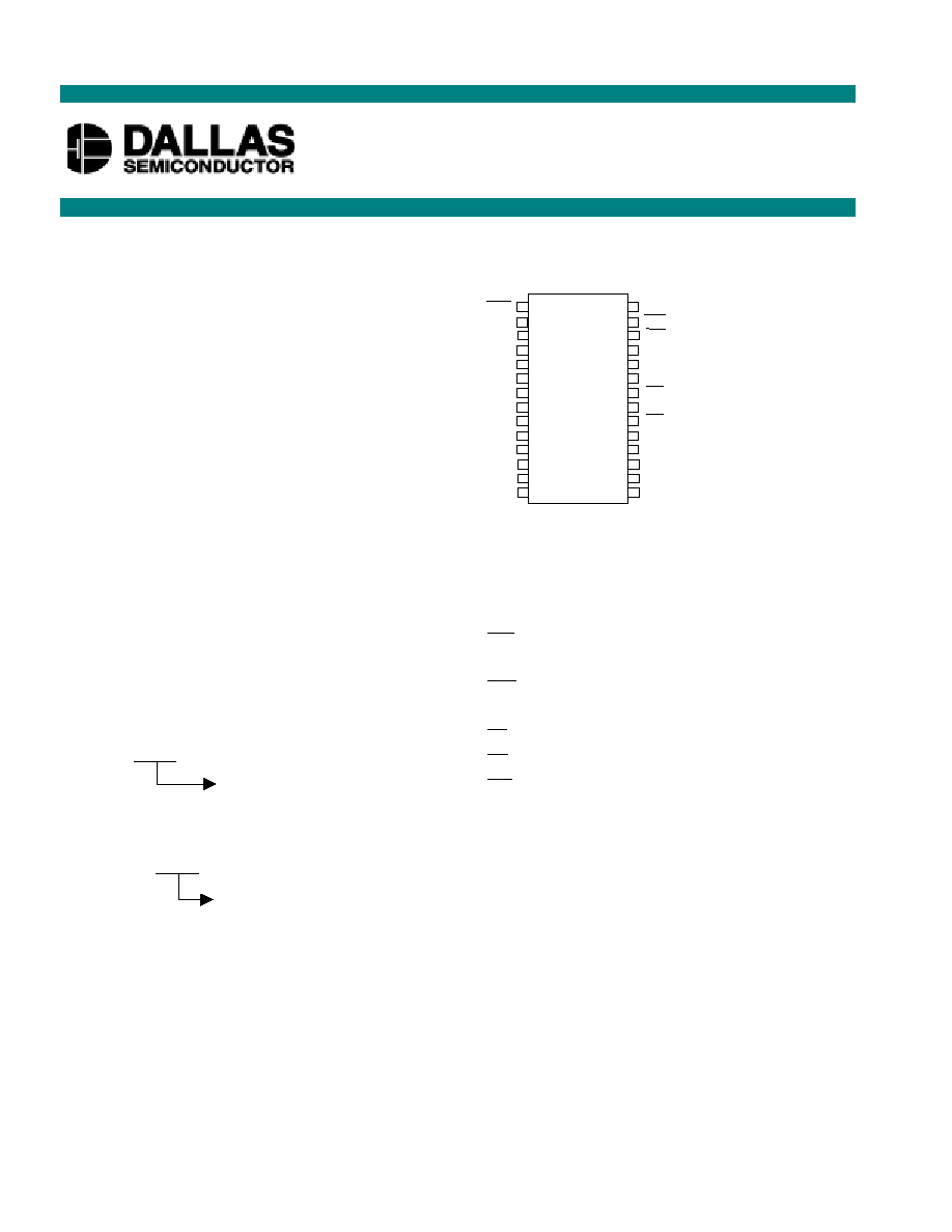
PIN ASSIGNMENT
PIN DESCRIPTION
A0-A12 -
Address
Input
DQ0-DQ7 -
Data
Input/Outputs
IRQ
\FT
- Interrupt, Frequency Test
Output (Open-Drain)
RST
- Power-On Reset Output
(Open-Drain)
CE
- Chip Enable
OE
- Output Enable
WE
- Write Enable
V
CC
- Power Supply Input
GND -
Ground
NC
- No Connection
DS1543
64k NV Timekeeping RAM
PRELIMINARY
www.dalsemi.com
V
CC
WE
IRQ/FT
A8
A9
A11
OE
A10
CE
DQ7
DQ6
DQ5
DQ4
DQ3
1
2
3
4
5
6
7
8
9
10
11
12
13
14
RST
A12
A7
A6
A5
A4
A3
A2
A1
A0
DQ0
DQ1
DQ2
GND
28
27
26
25
24
23
22
21
20
19
18
17
16
15
28-Pin Encapsulated Package
(700 Mil Extended)

DS1543
2 of 17
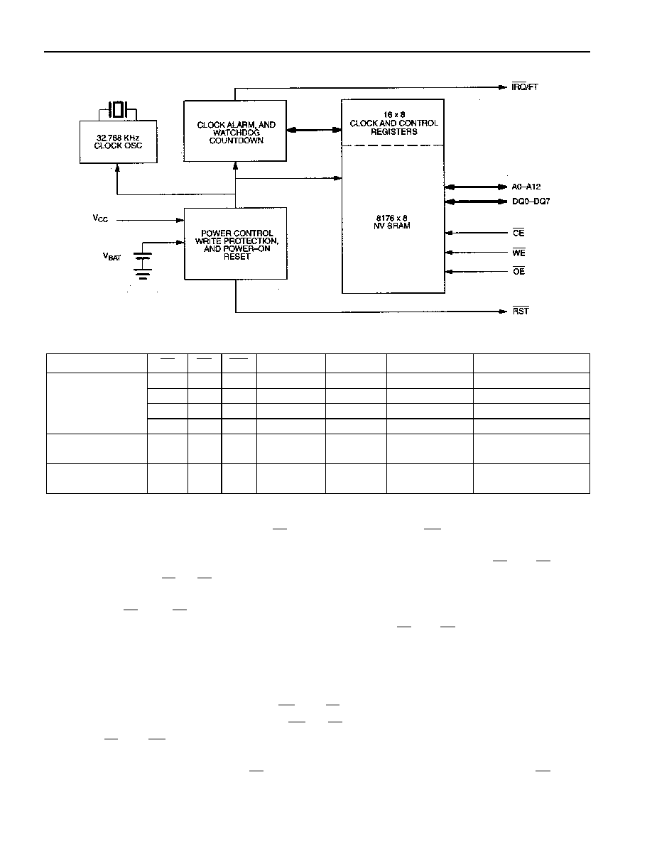
DESCRIPTION
The DS1543 is a full-function real-time clock/calendar (RTC) with a RTC alarm, watchdog timer, power-
on reset, battery monitor, and 8k x 8 non-volatile static RAM. User access to all registers within the
DS1543 is accomplished with a bytewide interface as shown in Figure 1. The RTC registers contain year,
month, date, day, hours, minutes, and seconds data in 24-hour BCD format. Corrections for day of month
and leap year are made automatically.
The RTC registers are double-buffered into an internal and external set. The user has direct access to the
external set. Clock/calendar updates to the external set of registers can be disabled and enabled to allow
the user to access static data. Assuming the internal oscillator is turned on, the internal set of registers are
continuously updated; this occurs regardless of external registers settings to guarantee that accurate RTC
information is always maintained.
The DS1543 has interrupt (
IRQ
/FT) and reset (
RST
) outputs which can be used to control CPU activity.
The
IRQ
/FT interrupt output can be used to generate an external interrupt when the RTC register values
match user programmed alarm values. The interrupt is always available while the device is powered from
the system supply and can be programmed to occur when in the battery backed state to serve as a system
wake-up. Either the
IRQ
/FT or
RST
outputs can also be used as a CPU watchdog timer, CPU activity is
monitored and an interrupt or reset output will be activated if the correct activity is not detected within
programmed limits. The DS1543 power-on reset can be used to detect a system power down or failure
and hold the CPU in a safe reset state until normal power returns and stabilizes; the
RST
output is used
for this function.
The DS1543 also contains its own power fail circuitry which automatically deselects the device when the
V
CC
supply enters an out of tolerance condition. This feature provides a high degree of data security
during unpredictable system operation brought on by low V
CC
levels.
PACKAGES
The DS1543 is available in two packages (28-pin DIP and 34-pin PowerCap module). The 28-pin DIP
style module integrates the crystal, lithium energy source, and silicon all in one package. The 34-pin
PowerCap module board is designed with contacts for connection to a separate PowerCap (DS9034PCX)
that contains the crystal and battery. This design allows the Power-Cap to be mounted on top of the
DS1543P after the completion of the surface mount process. Mounting the PowerCap after the surface
mount process prevents damage to the crystal and battery due to the high temperatures required for solder
reflow. The PowerCap is keyed to prevent reverse insertion. The PowerCap Module board and
PowerCap are ordered separately and shipped in separate containers. The part number for the PowerCap
is DS9034PCX.
DS1543
3 of 17
DS1543 BLOCK DIAGRAM Figure 1
DS1543 OPERATING MODES Table 1
V
CC
CE
OE
WE
DQ0-DQ7
A0-A12
MODE
POWER
V
IH
X
X
HIGH-Z
X
DESELECT
STANDBY
V
IL
X
V
IL
D
IN
A
IN
WRITE
ACTIVE
V
IL
V
IL
V
IH
D
OUT
A
IN
READ
ACTIVE
In Tolerance
V
IL
V
IH
V
IH
HIGH-Z
A
IN
READ
ACTIVE
V
BAT
< V
CC
<
Tolerance
X
X
X
HIGH-Z
X
DESELECT
CMOS STANDBY
<V
BAT
X
X
X
HIGH-Z
X
DATA
RETENTION
BATTERY
CURRENT
DATA READ MODE
The DS1543 is in the read mode whenever
CE
(chip enable) is low and
WE
(write enable) is high. The
device architecture allows ripple through access to any valid address location. Valid data will be
available at the DQ pins within t
AA
after the last address input is stable, providing that
CE
and
OE
access
times are satisfied. If
CE
or
OE
access times are not met, valid data will be available at the latter of chip
enable access (t
CEA
) or at output enable access time (t
OEA
). The state of the data input/output pins (DQ) is
controlled by
CE
and
OE
. If the outputs are activated before t
AA
, the data lines are driven to an
intermediate state until t
AA
. If the address inputs are changed while
CE
and
OE
remain valid, output data
will remain valid for output data hold time (t
OH
) but will then go indeterminate until the next address
access.
DATA WRITE MODE
The DS1543 is in the write mode whenever
WE
and
CE
are in their active state. The start of a write is
referenced to the latter occurring transition of
WE
or
CE
. The addresses must be held valid throughout
the cycle.
CE
and
WE
must return inactive for a minimum of t
WR
prior to the initiation of a subsequent
read or write cycle. Data in must be valid t
DS
prior to the end of the write and remain valid for t
DH
afterward. In a typical application, the
OE
signal will be high during a write cycle. However,
OE
can be

DS1543
4 of 17
active provided that care is taken with the data bus to avoid bus contention. If
OE
is low prior to
WE
transitioning low, the data bus can become active with read data defined by the address inputs. A low
transition on
WE
will then disable the outputs t
WEZ
after
WE
goes active.
DATA RETENTION MODE
The 5-volt device is fully accessible and data can be written and read only when V
CC
is greater than V
PF
.
However, when V
CC
is below the power-fail point V
PF
(point at which write protection occurs) the
internal clock registers and SRAM are blocked from any access. When V
CC
falls below the battery switch
point V
SO
(battery supply level), device power is switched from the V
CC
pin to the internal backup lithium
battery. RTC operation and SRAM data are maintained from the battery until V
CC
is returned to nominal
levels.
The 3.3-volt device is fully accessible and data can be written and read only when V
CC
is greater than
V
PF
. When V
CC
falls below V
PF
, access to the device is inhibited. If V
PF
is less than V
BAT
, the device
power is switched from V
CC
to the internal backup lithium battery when V
CC
drops below V
PF
If V
PF
is
greater than V
BAT
, the device power is switched from V
CC
to the internal backup lithium battery when
V
CC
drops below V
BAT
. RTC operation and SRAM data are maintained from the battery until V
CC
is
returned to nominal levels.
All control, data, and address signals must be powered down when V
CC
is powered down.
BATTERY LONGEVITY
The DS1543 has a lithium power source that is designed to provide energy for the clock activity, and
clock and RAM data retention when the V
CC
supply is not present. The capability of this internal power
supply is sufficient to power the DS1543 continuously for the life of the equipment in which it is
installed. For specification purposes, the life expectancy is 10 years at 25
∞
C with the internal clock
oscillator running in the absence of V
CC
Each DS1543 is shipped from Dallas Semiconductor with its
lithium energy source disconnected, guaranteeing full energy capacity. When V
CC
is first applied at a
level greater than V
PF
the lithium energy source is enabled for battery backup operation. Actual life
expectancy of the DS1543 will be much longer than 10 years since no internal battery energy is
consumed when V
CC
is present. In fact, in most applications, the life expectancy of the DS1543 will be
approximately equal to the shelf life (expected useful life of the internal lithium battery with no load
attached) of the battery which may prove to be as long as 20 years.
INTERNAL BATTERY MONITOR
The DS15433 constantly monitors the battery voltage of the internal batter. The Battery Low Flag (BLF)
bit of the Flags register (B4 of 1FF0h) is not writable and should always be a 0 when read. If a 1 is ever
present, an exhausted lithium energy source is indicated and both the contents of the RTC and RAM are
questionable.
POWER-ON RESET
A temperature-compensated comparator circuit monitors the level of V
CC
When V
CC
falls to the power
fail trip point, the
RST
signal (open-drain) is pulled low. When V
CC
returns to nominal levels, the
RST
signal continues to be pulled low for a period of 40 ms to 200 ms. The power-on reset function is
independent of the RTC oscillator and thus is operational whether or not the oscillator is enabled.
CLOCK OPERATIONS
Table 2 and the following paragraphs describe the operation of RTC, Alarm, and Watchdog functions.
DS1543
5 of 17
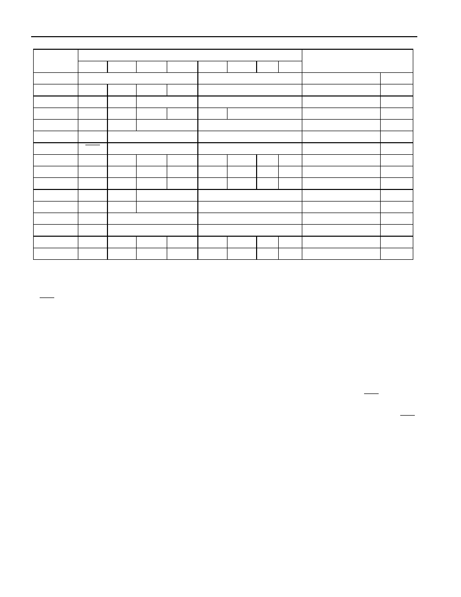
DS1543 REGISTER MAP Table 2
DATA
ADDRESS
B
7
B
6
B
5
B
4
B
3
B
2
B
1
B
0
FUNCTION/RANGE
1FFFh
10 Year
YEAR
YEAR
00-99
1FFEh
X
X
X
10 M
MONTH
MONTH
01-12
1FFDh
X
X
10 Date
DATE
DATE
01-31
1FFCh
X
FT
X
X
X
DAY
DAY
01-07
1FFBh
X
X
10 HOUR
HOUR
HOUR
00-23
1FFAh
X
10 MINUTES
MINUTES
MINUTES
00-59
1FF9h
OSC
10 SECONDS
SECONDS
SECONDS
00-59
1FF8h
W
R
Y
Y
Y
Y
Y
Y
CONTROL
1FF7h
WDS
BMB4
BMB3
BMB2
BMB1
BMB0
RB1
RB0
WATCHDOG
1FF6h
AE
Y
ABE
Y
Y
Y
Y
Y
INTERRUPTS
1FF5h
AM4
Y
10 DATE
DATE
ALARM DATE
01-31
1FF4h
AM3
Y
10 HOURS
HOURS
ALARM HOURS
00-23
1FF3h
AM2
10 MINUTES
MINUTES
ALARM MINUTES
00-59
1FF2h
AM1
10 SECONDS
SECONDS
ALARM SECONDS
00-59
1FF1h
Y
Y
Y
Y
Y
Y
Y
Y
UNUSED
1FF0h
WF
AF
0
BLF
0
0
0
0
FLAGS
X = Unused, read/writable under Write and Read
AE = Alarm Flag Enable
bit control
Y = Unused, read/writable without Write and
FT = Frequency Test bit
bit control
OSC
= Oscillator start/stop bit
ABE = Alarm in battery Back-up mode enable
W = Write bit
AM1-AM4 = Alarm Mask bits
R = Read bit
WF = Watchdog Flag
WDS = Watchdog Steering bit
AF = Alarm Flag
BMB0-BMB4 = Watchdog Multiplier bits
0 = "0" and are read only
RB0-RB1 = Watchdog Resolution bits
BLF = Battery Low Flag
CLOCK OSCILLATOR CONTROL
The Clock oscillator may be stopped at any time. To increase the shelf life of the backup lithium battery
source, the oscillator can be turned off to minimize current drain from the battery. The
OSC
bit is the
MSB of the seconds register (B7 of 1FF9h). Setting it to a 1 stops the oscillator, setting to a 0 starts the
oscillator. The DS1543 is shipped from Dallas Semiconductor with the clock oscillator turned off,
OSC
bit set to a 1.
READING THE CLOCK
When reading the RTC data, it is recommended to halt updates to the external set of double-buffered RTC
registers. This puts the external registers into a static state allowing data to be read without register
values changing during the read process. Normal updates to the internal registers continue while in this
state. External updates are halted when a 1 is written into the read bit, B6 of the Control register (1FF8h).
As long as a 1 remains in the Control register read bit, updating is halted. After a halt is issued, the
registers reflect the RTC count (day, date, and time) that was current at the moment the halt command
was issued. Normal updates to the external set of registers will resume within 1 second after the read bit
is set to a 0.