1 of 20
100101
FEATURES
ß Two linear taper potentiometers
- DS1855-010 (one 10k, 100 position and
one 10k, 256 position)
- DS1855-020 (one 10k, 100 position and
one 20k, 256 position)
- DS1855-050 (one 10k, 100 position and
one 50k, 256 position)
- DS1855-100 (one 10k, 100 position and
one 100k, 256 position)
ß 256 bytes of EEPROM memory
ß Access to data and potentiometer control via
a 2-wire interface
ß External write-protect pin to protect data and
potentiometer settings
ß Data and potentiometer settings also can be
write-protected through software control
ß Nonvolatile wiper storage
ß Operates from 3V or 5V supplies
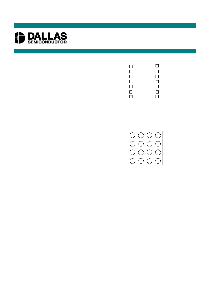
ß Packaging: 14-pin TSSOP, 16-ball STPBGA,
flip-chip package
ß Industrial operating temperature:
-40∫C to +85∫C
ß Programming temperature: 0∫C to +85∫C
DESCRIPTION
The DS1855 dual nonvolatile (NV) digital potentiometer and secure memory consists of one
100-position
linear taper potentiometer, one
256-position linear taper potentiometer, 256 bytes of EEPROM memory,
and a 2-wire interface. The DS1855, which features a new software write protect, is an upgrade of the
DS1845. The DS1855 provides an ideal method for setting bias voltages and currents in control
applications using a minimum of circuitry. The EEPROM memory allows a user to store configuration or
calibration data for a specific system or device as well as provide control of the potentiometer wiper
settings. Any type of user information may reside in the first 248 bytes of this memory. The next two
addresses of EEPROM memory are for potentiometer settings and the remaining 6 bytes of memory are
reserved. These reserved and potentiometer registers should not be used for data storage. Access to this
EEPROM is via an industry-standard 2-wire bus. The interface I/O pins consist of SDA and SCL. The
wiper position of the DS1855, as well as EEPROM data, can be write-protected through hardware using
the write-protect input pin (WP) or software using the 2-wire interface.
DS1855
Dual Nonvolatile Digital Potentiometer
and Secure Memory
www.maxim-ic.com
SDA
1
14
Vcc
SCL
2
13
H0
A0
3
12
W1
A1
4
11
H1
A2
5
10
L1
WP
6
9
W0
GND
7
8
L0
14-Pin TSSOP (173-mil)
A
B
C
D
1 2 3 4
Top View
16-Ball STPBGA (4mm x 4mm)
14-Pin Flip Chip (100-mil x 100-mil)
(Not Shown)

DS1855
2 of 20
PIN DESCRIPTIONS
Name TSSOP BGA
Description
V
CC
14
A3
Power Supply Terminal. The DS1855 will support supply
voltages ranging from +2.7V to +5.5V.
GND
7
D1
Ground Terminal.
SDA
1
B2
2-Wire serial data interface. The serial data pin is for serial data
transfer to and from the DS1855. The pin is open drain and may
be wire-ORed with other open drain or open collector interfaces.
SCL
2
A2
2-Wire Serial Clock Input. The serial clock input is used to
clock data into the DS1855 on rising edges and clock data out on
falling edges.
WP
6
C1
Write Protect Input. If set to logic 0, the data in memory and the
potentiometer wiper setting may be changed. If set to logic 1, both
the memory and the potentiometer wiper settings will be write
protected. The WP pin is pulled high internally.
A0
3 A1
Address Input. Pins A0, A1, and A2 are used to specify the
address of each DS1855 when used in a multi-dropped
configuration. Up to eight DS1855s may be addressed on a single
2-wire bus.
A1
4 B1
Address Input.
A2
5 C2
Address Input.
H0
13
A4
High terminal of Potentiometer 0. For both potentiometers, it is
not required that the high terminal be connected to a potential
greater than the low terminal. Voltage applied to the high terminal
of each potentiometer cannot exceed V
CC
or go below ground.
H1
11
B3
High terminal of Potentiometer 1.
L0
8
D3
Low terminal of Potentiometer 0. For both potentiometers, it is
not required that the low terminal be connected to a potential less
than the high terminal. Voltage applied to the low terminal of each
potentiometer cannot exceed V
CC
or go below ground.
L1
10 C4
Low terminal of Potentiometer 1.
W0
9
D4
Wiper terminal of Pot 0. The wiper position of Potentiometer 0
is determined by the byte at EEPROM memory location F9h.
Voltage applied to the wiper terminal of each potentiometer cannot
exceed the power supply voltage, V
CC
, or go below ground.
W1
12
B4
Wiper terminal of Pot 1. The wiper position of Potentiometer 1
is determined by the byte at EEPROM memory location F8h.
NC
C3
No Connect.
NC
D2
No Connect.

DS1855
3 of 20
DS1855 BLOCK DIAGRAM Figure 1
Up to eight DS1855s can be installed on a single 2-wire bus. Access to an individual device is achieved
by using a device address that is determined by the logic levels of address pins A0 through A2.
Additionally, the DS1855 will operate from 3V or 5V supplies. Three package options are available: 14-
pin TSSOP, 16-ball STPBGA, and flip-chip package.
V
CC
GND
SDA
SCL
WP
A0
A1
A2
H0
W0
L0
H1
W1
L1
248 BYTES
EEPROM
MEMORY
1 BYTE WIPER
SETTING
POT 0
1 BYTE WIPER
SETTING
POT 1
CONFIGURATION
BYTE
LOCK BYTE
LOCK BYTE
RESERVED
CONTROL
DATA
POTENTIOMETER 0
2-WIRE
INTERFACE
POTENTIOMETER 1
100-
Position
Pot
256-
Position
Pot

DS1855
4 of 20
MEMORY ORGANIZATION
The DS1855's serial EEPROM is internally organized with 256 words of 1 byte each. Each word requires
an 8-bit address for random word addressing. The byte at address F9h determines the wiper setting for
potentiometer 0, which contains 100 positions. Writing values above 63h to this address sets the wiper to
its uppermost position, but the MSB is ignored. The byte at address F8h determines the wiper setting for
potentiometer 1, which contains 256 positions (00h to FFh). Address locations FAh though FFh are
reserved and should not be written.
MEMORY
LOCATION
NAME OF
MEMORY
LOCATION
FUNCTION OF MEMORY LOCATION
00h ≠ F7h
User Memory
General-purpose user memory.
F8h
Potentiometer 1 Setting Writing to this byte controls the setting of potentiometer 1, a 256-
position pot. Valid settings are 00h to FFh.
F9h
Potentiometer 0 Setting Writing to this byte controls the setting of potentiometer 0, a 100-
position pot.
Valid settings are 00h to 63h. MSB is ignored.
FAh
Software Lock
Configuration Byte
The three lower bits in this byte can be used to set write-protection
to the 256-byte memory block.
B2: Writing this bit to a 1 protects the upper page of memory. If
this bit is set, memory locations F8h to FFh are configured for
write-protection.
B1: Writing this bit to a 1 protects the upper block of memory. If
this bit is set, memory locations 80h to F7h are configured for
write-protection. The upper page must be unlocked in order to
modify the locking of this portion of memory.
B0: Writing this bit to a 1 protects the lower block of memory. If
this bit is set, memory locations 00h to 7Fh are configured for
write-protection. The upper page must be unlocked in order to
modify the locking of this portion of memory.
B2 B1 B0

DS1855
5 of 20
FBh ≠ FCh
Lock Bytes
Writing to these two bytes allows the user to lock or unlock the
memory described in byte FAh.
LOCK: If memory location FBh is written to 56h and memory
location FCh is written to 25h, the device will enter lock mode.
Write protection will become active in the memory locations that
are specified in FAh.
UNLOCK: If memory location FBh is written to 67h and memory
location FCh is written to 36h, the device will be unlocked. Once
unlocked, the user can change the setting of memory location FAh
to affect the EEPROM write-protection.
The locking can be updated at any time as long as the upper
page is unlocked.
FD ≠ FFh
Reserved
Reserved