 | ÐлекÑÑоннÑй компоненÑ: DS2127 | СкаÑаÑÑ:  PDF PDF  ZIP ZIP |
Äîêóìåíòàöèÿ è îïèñàíèÿ www.docs.chipfind.ru
General Description
The DS2127 Ultra3 LVD/SE SCSI terminator provides
low-voltage differential (LVD)/single-ended (SE) termi-
nations for 14 SCSI lines. Through the voltage on the
DIFF_CAP pin, the device detects the types of drivers
on the bus. If the device is connected in an LVD-only
bus, the DS2127 provides LVD termination. If any sin-
gle-ended devices are connected to the bus, the
DS2127 uses SE termination. If any high-voltage differ-
ential (HVD) devices are connected to the bus, the
DS2127 isolates itself from the SCSI bus. The mode
change has a built-in delay that is determined by an
integrated SPI-3 mode change filter/delay. The termi-
nating resistors can also be disconnected from the bus
by asserting the ISO pin.
For the LVD termination, the DS2127 provides 14 pre-
cisely trimmed resistors. Each resistor is biased with
two current sources to a fail-safe state. For SE termina-
tion, the DS2127 provides 14 precision 110
resistors
and one regulator for active-negation bias.
Applications
SCSI Array Backplane
SCSI Cables
Features
Fully Compliant with Ultra2, Ultra3, Ultra160, and
Ultra320 SCSI Standards
Provides LVD/SE Termination for 14 Signal Pairs
Auto-Selection of LVD or SE Termination
5% Tolerance on SE and LVD Termination
Resistance
Low 3pF Power-Down Capacitance
Built-In Mode-Change Filter/Delay
On-Board Thermal-Shutdown Circuitry
SCSI Bus Hot-Plug Compatible
Fully Supports Actively Negated SE SCSI Signals
DS2127
Ultra3 LVD/SE SCSI 14-Line Terminator
______________________________________________ Maxim Integrated Products
1
R13N
R13P
R12N
R12P
R11N
R11P
R10N
R10P
R9N
R9P
R8N
R8P
R2P
R2N
R3P
R3N
R4P
R4N
R5P
R5N
R6P
R6N
R7P
R7N
13
14
15
16
17
18
19
20
21
22
23
24
48
47
46
45
44
43
42
41
40
39
38
37
LQFP
GND
SE
LVD
HS_GND
HS_GND
HS_GND
HS_GND
HS_GND
HS_GND
DIFF_CAP
DIFFSENS
ISO
25
26
27
28
29
30
31
32
33
34
35
36
12
11
10
9
8
7
6
5
4
3
2
1
R1N
R1P
V
REF
HS_GND
HS_GND
HS_GND
HS_GND
HS_GND
HS_GND
TPWR
R14N
R14P
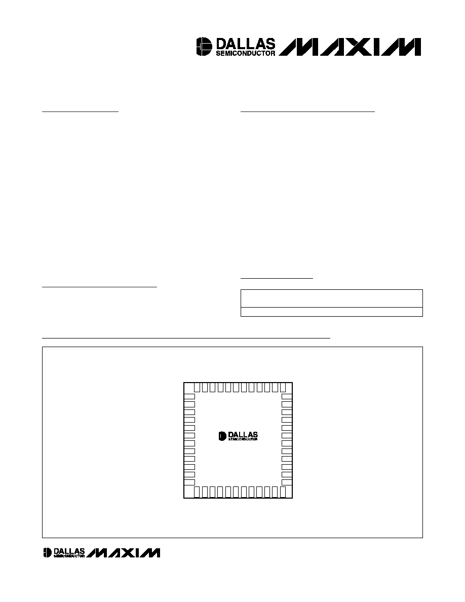
DS2127
TOP VIEW
Pin Configuration
Ordering Information
Rev 1; 3/04
For pricing, delivery, and ordering information, please contact Maxim/Dallas Direct! at
1-888-629-4642, or visit Maxim's website at www.maxim-ic.com.
PART
TEMP RANGE
PIN-
PACKAGE
TOP
MARK
DS2127
0°C to +70
°C
48 LQFP
DS2127

DS2127
Ultra3 LVD/SE SCSI 14-Line Terminator
2
_____________________________________________________________________
ABSOLUTE MAXIMUM RATINGS
ELECTRICAL CHARACTERISTICS
(TPWR = V
TPWR(MIN)
to V
TPWR(MAX)
, T
A
= 0°C to +70°C, unless otherwise noted.)
Stresses beyond those listed under "Absolute Maximum Ratings" may cause permanent damage to the device. These are stress ratings only, and functional
operation of the device at these or any other conditions beyond those indicated in the operational sections of the specifications is not implied. Exposure to
absolute maximum rating conditions for extended periods may affect device reliability.
Voltage Range on All Pins Relative to Ground ......-0.3V to +6.0V
V
REF
Continuous Output Current....................................±200mA
Operating Temperature Range...............................0°C to +70°C
Junction Temperature ......................................................+150°C
Storage Temperature Range .............................-65°C to +160°C
Soldering Temperature .......................................See IPC/JEDEC
J-STD-020A Specification
PARAMETER
SYMBOL
CONDITIONS
MIN
TYP
MAX
UNITS
LVD
2.7
3.3
5.5
TPWR Operating Supply Range
(Note 1)
V
TPWR
SE
4
5.0
5.5
V
TPWR SUPPLY CURRENT
I
TPWR_LVD
LVD SCSI mode
32
I
TPWR_SE
SE SCSI mode
10
mA
TPWR Supply Current (All Lines
Open)
I
TPWR_ISO
ISO mode (terminators disabled)
750
µA
LVD TERMINATION (Applies to each line pair, 1 to 14 in LVD mode)
Differential-Mode Termination
Resistance
R
DM
100
110
Common-Mode Termination
Resistance
R
CM
R
P
and R
N
shorted together
(V
CM(MAX)
= 2V, V
CM(MIN)
= 0.5V)
110
165
Differential-Mode Bias
V
DM
All lines open
100
125
mV
Common-Mode Bias
V
CM
R
P
and R
N
shorted together (Note 1)
1.15
1.25
1.35
V
SE TERMINATION (Applies to single-ended terminators, 1 to 14 in SE mode)
Single-Ended Mode Termination
Resistance
R
SE
R
SE
= (V
LX
- 0.2) / I
LX
, where V
LX
= voltage
at terminator pin with pin unloaded and
I
LX
= current for each terminator pin with
the pin forced to 0.2V
104.5
110
115.5
Signal level at 0.2V, all lines low
-21
-24
-25.4
Termination Current
I
SE
Signal level at 0.5V
-18
-22.4
mA
SE Voltage Reference
V
REF
2.7
2.85
3.0
V
Pin Leakage
With ISO high
400
nA
Single-Ended GND Resistance
R
GND
Measured at R
P
pins, I = 10mA
20
60
TERMINATOR PIN CAPACITANCE
Terminator Pin Capacitance
C
IN
With ISO high (Note 2)
3
pF
V
REF
REGULATOR
1.25V Regulator Output Voltage
V
REF_LVD
0.5V
V
CM
2.0V, V
CM
applied to all R
P
and R
N
lines simultaneously
1.15
1.25
1.35
V
1.25V Regulator Short-Circuit
Source Current
I
SOURCE
V
REF
= 0V
-375
-700
-1000
mA
1.25V Regulator Short-Circuit
Sink Current
I
SINK
V
REF
= 3.3V
170
300
700
mA
DS2127
Ultra3 LVD/SE SCSI 14-Line Terminator
_____________________________________________________________________
3
Note 1: All voltages are referenced to ground.
Note 2: Guaranteed by design and not production tested.
Note 3: Room temperature only.
ELECTRICAL CHARACTERISTICS (continued)
(TPWR = V
TPWR(MIN)
to V
TPWR(MAX)
, T
A
= 0°C to +70°C, unless otherwise noted.)
PARAMETER
SYMBOL
CONDITIONS
MIN
TYP
MAX
UNITS
V
REF
REGULATOR
1.25V Regulator Line Regulation
V
REF
unloaded; vary TPWR from
2.7V to 5.5V
1.0
2.5
%
2.85V Regulator
2.7
2.85
3.0
V
2.85V Regulator Short-Circuit
Source Current
V
REF
= 0V
-375
-700
-1000
mA
2.85V Regulator Short-Circuit
Sink Current
V
REF
= 3.3V
170
300
700
mA
2.85V Regulator Line Regulation
V
REF
unloaded; vary TPWR from
2.7V to 5.5V
1.0
2.5
%
DIFFSENS OUTPUT
DIFFSENS Driver Output Voltage
V
DSO
-5mA
I
DIFFSENS
50µA
1.2
1.4
V
DIFFSENS Driver Source Current
I
DSH
V
DIFFSENS
= 0V
-15
-5
mA
DIFFSENS Driver Sink Current
I
DSL
V
DIFFSENS
= 2.75V
100
200
µA
I
LEAK,
LOW
With ISO high, |V
DIFFSENS
| = 0.3V
-3
+1
DIFFSENS Leakage (Note 3)
I
LEAK,
HIGH
With ISO high, |V
DIFFSENS
- V
TPWR
| = 0.3V
1
3
µA
THERMAL SHUTDOWN
Thermal-Shutdown Threshold
For increasing temperature
130
°C
Thermal-Shutdown Hysteresis
10
°C
MODE CHANGE DELAY/FILTER
Mode Change Delay
t
DELAY
0.66
1.25
2.00
ms
LOGICAL SIGNALS (ISO)
Input Low Voltage
V
IL
-0.3
+0.8
V
Input High Voltage
V
IH
2.0
TPWR + 0.3
V
Input Current
I
IL
V
CC
= 3.3V
-30
-10
µA
STATUS BITS (LVD, SE)
Source Current
I
OH
V
CC
= 3.3V, V
LOAD
= 2.4V
-4
-6
mA
Sink Current
I
OL
V
CC
= 3.3V, V
LOAD
= 0.4V
2
5
mA
DIFF_CAP
Input Current
IL
V
IL
= -0.3V
-1
+1
µA
DIFF_CAP SE Operating Range
V
SEOR
-0.3
+0.5
V
DIFF_CAP LVD Operating Range
V
LVDOR
0.7
1.9
V
DIFF_CAP HVD Operating Range
V
HVDOR
2.4
V
TPWR
+ 0.3
V
DS2127
Ultra3 LVD/SE SCSI 14-Line Terminator
4
_____________________________________________________________________
Pin Description
PIN
NAME
FUNCTION
1, 2, 1124,
3748
R_ _ P, R_ _ N
Signal Termination. Connect to SCSI bus signal lines. Asserting ISO removes the terminators from the
SCSI bus. R_ _ P pins are the ground line for SE operation and the positive lines in differential mode.
R_ _ N pins are the signal lines in SE operation and the negative lines in differential mode.
3
TPWR
Termination Power. Connect to the SCSI TERMPWR line and decouple with a ceramic
2.2µF capacitor.
49, 2833
HS_GND
Heat-Sink Ground. Internally connected to the mounting pad. These pins must be connected to
ground. These pins should be connected to a ground plane with the layout optimized for
heat transfer.
10
V
REF
Regulator Output Voltage. This must be decoupled with a 4.7µF capacitor. Asserting ISO floats this
output. A high-frequency capacitor (0.1µF) should also be placed on the V
REF
pin in applications that
use fast rise/fall-time drivers.
25
GND
Signal Ground
26
SE
SE Mode Indicator. A high state indicates SE mode detected on SCSI bus.
27
LVD
LVD Mode Indicator. A high state indicates LVD mode detected on SCSI.
34
DIFF_CAP
DIFFSENSE Capacitor. Connect a 0.1µF capacitor for the DIFFSENSE filter. Input to detect the type of
device (differential or single-ended) on the SCSI bus.
35
DIFFSENS
DIFFSENSE. Output to drive the SCSI bus DIFFSENS line.
36
ISO
Isolation Input. When pulled high, terminating resistors and biasing current sources are removed from
the SCSI bus. When not connected to ground, the pin has a 10µA current source pulling the pin to the
high state.
2.15V
0.6V
THERMAL
SHUTDOWN
1.30V
DIFF_CAP
ISO
2.15V
1.30V
1.25V
(LVD)
R1N
R1P
R14N
R14P
V
REF
0.6V
DIFFSENS
2.85V
(SE)
LVD
SE
HVD
LVD SE HVD
LVD
SE
LVD
SE
CONTROL LOGIC
DELAY/
FILTER
BANDGAP
REFGEN AND
TRIM
10
µA
52
52
52
52
110
110
124
124
SE
ALL SWITCHES UP
HVD/ISO
ALL SWITCHES CENTER
LVD
ALL SWITCHES DOWN
DS2127
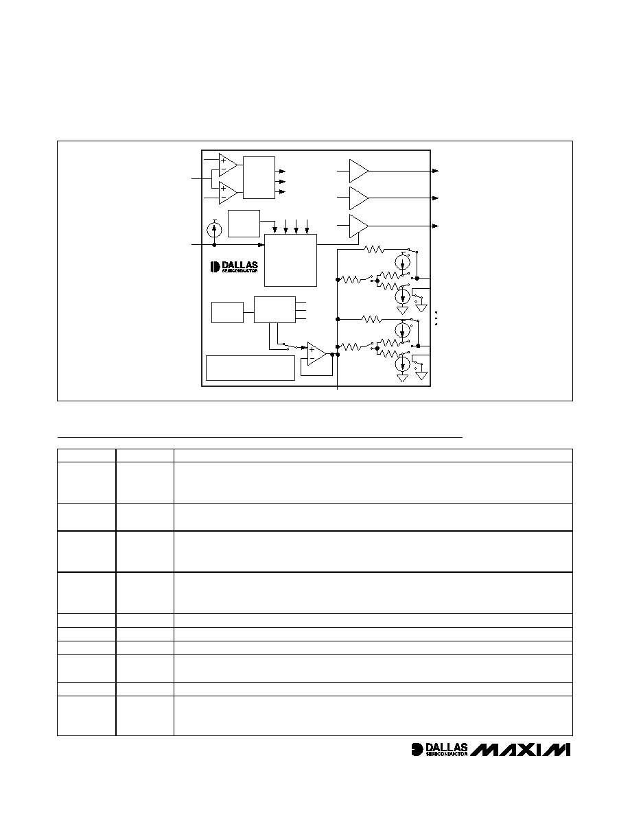
Figure 1. Block Diagram

Detailed Description
The DS2127 provides dual-mode active terminators
with auto-switching SE and LVD termination for 14 SCSI
lines. The DIFFSENSE signal performs mode detection
and selection.
In LVD mode, the termination configuration is a y-type
terminator with a 105
differential resistance and a
150
common-mode resistance. The termination resis-
tor is biased with two current sources and the common-
mode node is connected to a 1.25V voltage regulator.
A fail-safe bias of 112mV is maintained when no drivers
are connected to the SCSI bus.
In SE mode, each negative signal input pin is connect-
ed to 2.85V through a 110
resistor.
In HVD mode, the termination resistors are isolated
from the SCSI bus and the resistor pins are left floating.
The voltage regulator is powered down and the V
REF
pin is in a high-impedance state.
The DIFF_CAP pin is connected to the SCSI DIFFSENSE
line and monitors the voltage to determine the proper
operating mode of the device. Any DIFFSENSE voltage
below 0.5V indicates single ended; any DIFFSENSE volt-
age between 0.7V and 1.9V is LVD, and above 2.4V is
an HVD SCSI. On power-up, the DS2127 assumes SE
mode. If the voltage on the DIFF_CAP is between 0.7V
and 1.9V, the device waits t
DELAY
before entering the
LVD mode. The delay is the same when changing
modes. A new mode change can start at any time after a
previous mode change has been detected.
Typically, four DS2127s are used in a SCSI bus seg-
ment. On two chips, the DIFF_CAP inputs at each end
of the bus should be connected together. There should
be a 50Hz noise filter implemented on DIFF_CAP at
each end of the bus, as close as possible to the
DIFF_CAP pins. This filter consists of a 20k
resistor
between the DIFFSENS and DIFF_CAP pins, and a
0.1µF capacitor from DIFF_CAP to GND. See
Figure
2
for the typical operating circuit.
When ISO is connected to TPWR, the termination pins
are isolated from the SCSI bus and V
REF
becomes
inactive, and the device is in a low-power state. During
thermal shutdown, the termination pins are isolated
from the SCSI bus and V
REF
becomes high impedance.
The DIFFSENS driver is shut down during either of
these two events. LVD and SE signals indicate whether
the SCSI bus segment is in LVD or SE mode.
Chip Information
TRANSISTOR COUNT: 8114 CMOS and 87 Bipolar
PROCESS: BiCMOS
SUBSTRATE CONNECTED TO GROUND
Thermal Information
Thermal Resistance (junction-to-ambient):
JA
= +29°C/W
Thermal Resistance (junction-to-case):
JC
= +10°C/W
DS2127
Ultra3 LVD/SE SCSI 14-Line Terminator
_____________________________________________________________________
5
TPWR
ISO
TPWR
ISO
DIFF_CAP
DIFFSENS
4.7
µF
0.1
µF
4.7
µF
2.2
µF
2.2
µF
2.2
µF
2.2
µF
0.1
µF
DIFFSENS
20k
20k
V
REF
V
REF
V
REF
V
REF
DIFFSENS
DIFFSENS
ISO
GND
TPWR
ISO
GND
TPWR
DIFFSENS
DIFF_CAP
DIFF_CAP
DIFF_CAP
4.7
µF
4.7
µF
DATA LINES (8) + PARITY
DATA LINES (4) + PARITY
CONTROL LINES (9)
DATA LINES (4)
GND
GND
Figure 2. Typical Operating Circuit