 | ÐлекÑÑоннÑй компоненÑ: DS3906U | СкаÑаÑÑ:  PDF PDF  ZIP ZIP |
Äîêóìåíòàöèÿ è îïèñàíèÿ www.docs.chipfind.ru
General Description
The DS3906 is intended for low resistance, small step-
size applications. It contains three nonvolatile (NV), low-
temperature coefficient, variable digital resistors that
are capable of ohm and subohm increments when
used in parallel with a fixed external resistor. All three of
the DS3906's resistors have 64 positions (plus a high-Z
state) with a pseudo-log response cleverly chosen to
have a linear equivalent resistance when paired with an
external resistor (see graphs below). The DS3906 also
contains 16 bytes of user EEPROM that, in addition to
the resistors, are controlled through an I
2
CTM-compati-
ble serial interface. Three address pins allow up to
eight DS3906s to be placed on the same I
2
C bus.
The DS3906 can also be factory cutomized to provide a
variety of transfer functions depending on user
requirements. Contact mixedsignal.apps@dalsemi.com
for additional information.
Applications
Low Ohm, Fine Resolution Driver Control for LED
Display Panels
Low Ohm, Fine Resolution Instrumentation Control
Features
Three Programmable Resistors for Low Step-Size
Applications (Ohm and Subohm)
Resistor Settings are NV
16-Byte NV User Memory (EEPROM)
I
2
C-Compatible Serial Interface
Up to 8 Devices Can be Multidropped on the
Same I
2
C Bus
Low Power Consumption
Wide Operating Voltage (2.7V to 5.5V)
Operating Temperature Range: -40°C to +85°C
DS3906
Triple NV Low Step Size Variable
Resistor Plus Memory
______________________________________________ Maxim Integrated Products
1
TOP VEIW
10
1
A1
A2
9
2
SDA
A0
10-PIN
µSOP
8
3
H0
SCL
7
4
H1
V
CC
6
5
H2
GND
DS3906
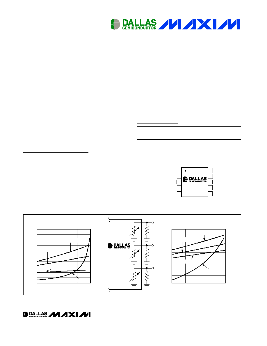
Pin Configuration
DS3906
R0
R
EXT0
R1
R
EXT1
R2
R
EXT2
RESISTOR 0 AND 1 RESISTANCE vs. POSITION
(WITH AND WITHOUT EXTERNAL RESISTOR)
RESISTOR POSITION (dec)
R
EFFECTIVE
= R
0, 1
|| R
EXT
(
)
R
0, 1
WITHOUT R
EXT
(
)
48
32
16
20
40
60
80
100
120
140
160
180
200
0
20
500
100
1500
2000
2500
3000
0
0
64
R
0, 1
|| (R
EXT
= 150
)
R
0, 1
|| (R
EXT
= 105
)
R
0, 1
|| (R
EXT
= 50
)
R
0, 1
WITHOUT R
EXT
RESISTOR 2 RESISTANCE vs. POSITION
(WITH AND WITHOUT EXTERNAL RESISTOR)
RESISTOR POSITION (dec)
R
EFFECTIVE
= R
2
|| R
EXT
(
)
48
32
16
50
100
150
200
250
300
350
0
0
64
R
2
WITHOUT R
EXT
(
)
600
800
1000
1200
1400
1600
400
R
2
|| (R
EXT
= 400
)
R
2
|| (R
EXT
= 310
)
R
2
|| (R
EXT
= 250
)
R
2
WITHOUT R
EXT
Resistor Plots
Rev 0; 4/05
For pricing, delivery, and ordering information, please contact Maxim/Dallas Direct! at
1-888-629-4642, or visit Maxim's website at www.maxim-ic.com.
+Denotes lead-free package.
Add "/T&R" for Tape-and-Reel orders
Ordering Information
Typical Operating Circuit appears at end of data sheet.
PART
TEMP RANGE
PACKAGE
DS3906U
-40°C to +85°C
10-Pin µSOP
DS3906U+
-40°C to +85°C
10-Pin µSOP
I
2
C is a trademark of Philips Corp. Purchase of I
2
C components of Maxim Integrated Products, Inc., or one of its sublicensed
Associated Companies, conveys a license under the Philips I
2
C Patent Rights to use these components in an I
2
C system, provided
that the system conforms to the I
2
C Standard Specification as defined by Philips Corp.
DS3906
Triple NV Low Step Size Variable
Resistor Plus Memory
2
_____________________________________________________________________
ABSOLUTE MAXIMUM RATINGS
RECOMMENDED OPERATING CONDITIONS
(T
A
= -40°C to +85°C)
Stresses beyond those listed under "Absolute Maximum Ratings" may cause permanent damage to the device. These are stress ratings only, and functional
operation of the device at these or any other conditions beyond those indicated in the operational sections of the specifications is not implied. Exposure to
absolute maximum rating conditions for extended periods may affect device reliability.
Voltage on V
CC
, SDA, SCL, and H0-H2 Pins
Relative to Ground.............................................-0.5V to +6.0V
Voltage on A0, A1, and A2
Relative to Ground .....-0.5V to V
CC
+ 0.5V, not to exceed +6.0V
Resistor Current ....................................................................5mA
Operating Temperature Range ...........................-40°C to +85°C
EEPROM Programming Temperature Range .........0°C to +70°C
Storage Temperature Range ............................-55°C to +125°C
Soldering Temperature...................See J-STD-020 Specification
PARAMETER
SYMBOL
CONDITIONS
MIN
TYP
MAX
UNITS
Supply Voltage
V
CC
(Note 1)
+2.7
+5.5
V
Input Logic 1
V
IH
0.7 x
V
CC
V
CC
+
0.3
V
Input Logic 0
V
IL
-0.3
0.3 x
V
CC
V
Resistor Inputs
H0, H1, H2 V
CC
= 2.7V to 5.5V
-0.3
+5.5
V
Resistor Current
I
R
5
mA
DC ELECTRICAL CHARACTERISTICS
(V
CC
= +2.7V to +5.5V, T
A
= -40°C to +85°C, unless otherwise noted.)
PARAMETER
SYMBOL
CONDITIONS
MIN
TYP
MAX
UNITS
3V
130
Standby Current (Note 2)
I
STBY
5V
160
250
µA
Input Leakage for All Pins
I
L
(Note 3)
-1.0
+1.0
µA
3mA sink current
0
0.4
Low-Level Output Voltage (SDA)
V
OL SDA
6mA sink current
0
0.6
V
I/O Capacitance
C
I/O
10
pF
ANALOG RESISTOR CHARACTERISTICS
(V
CC
= +2.7V to +5.5V, T
A
= -40°C to +85°C, unless otherwise noted.)
PARAMETER
SYMBOL
CONDITIONS
MIN
TYP
MAX
UNITS
Resistor Tolerance
From nominal values in Table 3
-20
+20
%
INL
(Note 4)
-2
+2
LSB
DNL
(Note 4)
-0.5
+0.5
LSB
Temperature Coefficient
At position 3Fh (Note 8)
60
ppm/°C
Resistor High-Z
R
HIGH-Z
5.5
M
Resistors
Guaranteed monotonic by design

DS3906
Triple NV Low Step Size Variable
Resistor Plus Memory
_____________________________________________________________________
3
NONVOLATILE MEMORY CHARACTERISTICS
(V
CC
= +2.7V to 5.5V)
PARAMETER
SYMBOL
CONDITIONS
MIN
TYP
MAX
UNITS
EEPROM Writes
0°C to +70°C. The room temperature
specification is at least 4x better than
specification over 0°C to +70°C.
50,000
AC ELECTRICAL CHARACTERISTICS (See Figure 2)
(V
CC
= +2.7V to 5.5V, T
A
= -40°C to +85°C, unless otherwise noted. Timing referenced to V
IL(MAX)
and V
IH(MIN)
.)
Note 1: All voltages referenced to ground.
Note 2: I
STBY
is specified with SDA = SCL = V
CC
, resistor pins floating, and inputs tied to V
CC
or GND.
Note 3: The DS3906 will not obstruct the SDA and SCL lines if V
CC
is switched off as long as the voltages applied to these input do
not violate their minimum and maximum input voltage levels.
Note 4: Tested with external resistor of 87
for R
0
and R
1
and 258
for R
2
at 25°C.
Note 5: Timing shown is for fast mode (400kHz) operation. This device is also backward compatible with I
2
C standard mode timing.
Note 6: C
B
total capacitance of one bus line in picofarads.
Note 7: The EEPROM write time begins after a stop condition occurs.
Note 8: Guaranteed by design.
PARAMETER
SYMBOL
CONDITIONS
MIN
TYP
MAX
UNITS
SCL Clock Frequency
f
SCL
(Note 5)
0
400
kHz
Bus Free Time Between Stop and
Start Conditions
t
BUF
1.3
µs
Hold Time (Repeated) Start
Condition
t
HD:STA
0.6
µs
Low Period of SCL
t
LOW
1.3
µs
High Period of SCL
t
HIGH
0.6
µs
Data Hold Time
t
HD:DAT
0
0.9
µs
Data Set-up Time
t
SU:DAT
100
ns
Start Set-up time
t
SU:STA
0.6
µs
SDA and SCL Rise Time
t
R
(Note 6)
20 +
0.1C
B
300
ns
SDA and SCL Fall Time
t
F
(Note 6)
20 +
0.1C
B
300
ns
Stop Set-up Time
t
SU:STO
0.6
µs
SDA and SCL Capacitive
Loading
C
B
(Note 6)
400
pF
EEPROM Write Time
t
WR
(Note 7)
20
ms
DS3906
Triple NV Low Step Size Variable
Resistor Plus Memory
4
_____________________________________________________________________
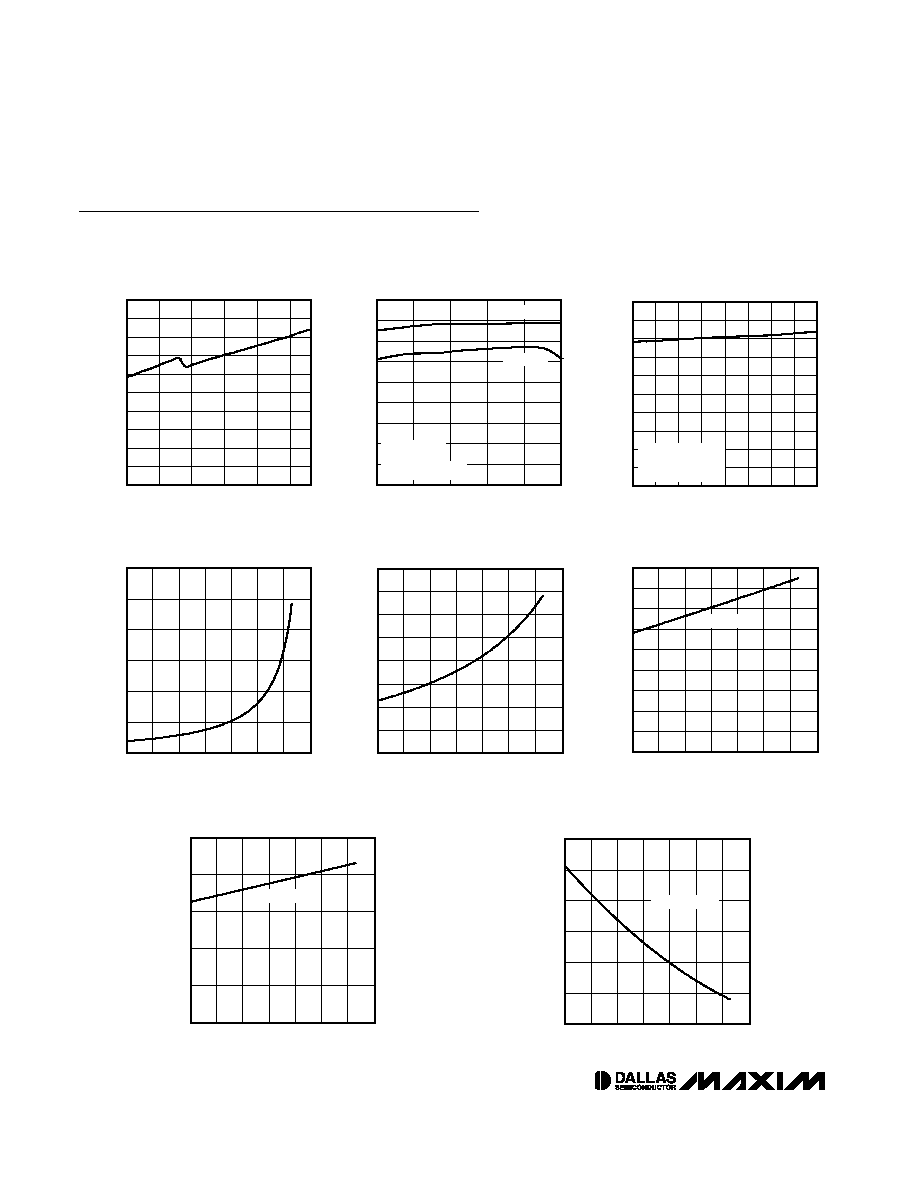
Typical Operating Characteristics
(V
CC
= +5.0V, T
A
= +25°C, unless otherwise noted.)
SUPPLY CURRENT
vs. SUPPLY VOLTAGE
DS3906 toc01
SUPPLY VOLTAGE (V)
SUPPLY CURRENT (
µ
A)
4.70
5.20
3.70
4.20
3.20
20
40
60
80
100
120
140
160
180
200
0
2.70
SUPPLY CURRENT
vs. TEMPERATURE
DS3906 toc02
TEMPERATURE (
°C)
SUPPLY CURRENT (
µ
A)
60
35
10
-15
20
40
60
80
100
120
140
160
180
0
-40
85
V
CC
= 5V
V
CC
= 3.3V
SDA/SCL = V
CC
ADDRESS PINS
CONNECTED TO GND
SUPPLY CURRENT
vs. SCL FREQUENCY
DS3902 toc03
SCL FREQUENCY (kHz)
SUPPLY CURRENT (
µ
A)
350
300
200 250
100 150
50
20
40
60
80
100
120
140
160
180
200
0
0
400
V
CC
= SDA = 5V
ADDRESS PINS
CONNECTED TO GND
RESISTORS (R
0,1
)
vs. RESISTOR SETTING
DS3906 toc04
RESISTOR SETTING (dec)
RESISTORS (R
0,1
) (
)
60
40
50
10
20
30
500
1000
1500
2000
2500
3000
0
0
70
RESISTOR R
2
vs. RESISTOR SETTING
DS3906 toc05
RESISTOR SETTING (dec)
RESISTOR (R
2
) (
)
200
400
600
800
1000
1200
1400
1600
0
60
40
50
10
20
30
0
70
RESISTANCE (R
0,1
R
EXT
)
vs. RESISTOR SETTING
DS3906 toc06
RESISTOR SETTING (dec)
RESISTANCE (R
0,1
R
EXT
) (
)
10
20
30
40
50
60
70
80
90
0
60
40
50
10
20
30
0
70
R
EXT
= 87
RESISTANCE (R
2
R
EXT
)
vs. RESISTOR SETTING
DS3906 toc07
RESISTOR SETTING (dec)
RESISTANCE (R
2
R
EXT
) (
)
50
100
150
200
250
0
60
40
50
10
20
30
0
70
R
EXT
= 258
RESISTOR R
0,1
TEMPERATURE COEFFICIENT
(-40
°C TO +25°C) vs. RESISTOR SETTING
DS3906 toc08
RESISTOR SETTING (dec)
RESISTOR R
0,1
TEMPERATURE COEFFICIENT (ppm/
°
C)
0
50
100
150
200
250
-50
60
40
50
10
20
30
0
70
-40
°C TO +25°C
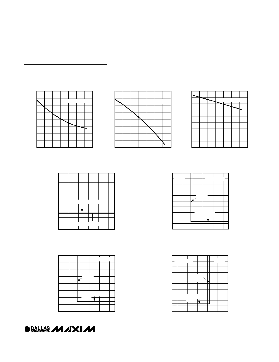
DS3906
Triple NV Low Step Size Variable
Resistor Plus Memory
_____________________________________________________________________
5
RESISTOR R
0,1
TEMPERATURE COEFFICIENT
(+25
°C TO +85°C) vs. RESISTOR SETTING
DS3906 toc09
RESISTOR SETTING (dec)
RESISTOR R
0,1
TEMPERATURE COEFFICIENT (ppm/
°
C)
50
100
150
200
250
300
350
400
0
60
40
50
10
20
30
0
70
+25
°C TO +85°C
RESISTOR R
2
TEMPERATURE COEFFICIENT
(-40
°C TO +25°C) vs. RESISTOR SETTING
DS3906 toc10
RESISTOR SETTING (dec)
RESISTOR R
2
TEMPERATURE COEFFICIENT (ppm/
°
C)
-20
-15
-10
-5
0
5
10
15
-25
60
40
50
10
20
30
0
70
-40
°C TO +25°C
RESISTOR R
2
TEMPERATURE COEFFICIENT
(+25
°C TO +85°C) vs. RESISTOR SETTING
DS3906 toc11
RESISTOR SETTING (dec)
RESISTOR R
2
TEMPERATURE COEFFICIENT (ppm/
°
C)
20
40
60
80
100
120
140
160
180
0
60
40
50
10
20
30
0
70
+25
°C TO +85°C
Typical Operating Characteristics (continued)
(V
CC
= +5.0V, T
A
= +25°C, unless otherwise noted.)
RESISTANCE
vs. SUPPLY VOLTAGE
DS3906 toc12
SUPPLY VOLTAGE (V)
RESISTANCE (
)
4.70
3.70
4.20
3.20
500
1000
1500
2000
0
2.70
5.20
RESISTOR R
2
AT POSITION 1Fh
RESISTOR R
0,1
AT POSITION 2Fh
R
0,1
RESISTANCE AT POSITION 2Fh
vs. POWER-UP VOLTAGE
DS3906 toc13
POWER-SUPPLY VOLTAGE (V)
R
0,1
RESISTANCE AT POSITION 2Fh (
)
3
4
2
1
500
1000
1500
2000
2500
3000
3500
4000
4500
5000
0
0
5
>5.5M
RESISTORS R
0,1
EEPROM
RECALL
PROGRAMMED
VALUE
R
2
RESISTANCE AT POSITION 1Fh
vs. POWER-UP VOLTAGE
DS3906 toc14
POWER-UP VOLTAGE (V)
R
2
RESISTANCE AT POSITION 1Fh (
)
4
5
2
1
3
500
1000
1500
2000
2500
3000
3500
4000
0
0
>5.5M
RESISTOR R
2
EEPROM
RECALL
PROGRAMMED
VALUE
R
0,1
RESISTANCE AT POSITION 2Fh
vs. POWER-UP VOLTAGE
DS3906 toc15
POWER-DOWN VOLTAGE (V)
R
0,1
RESISTANCE AT POSITION 2Fh (
)
1
2
3
4
5
50
100
150
200
250
300
350
400
450
500
0
0
0
>5.5M
RESISTOR R
0,1
EEPROM
RECALL
PROGRAMMED
VALUE