1 of 47
REV: 032003
Note: Some revisions of this device may incorporate deviations from published specifications known as errata. Multiple revisions of any device
may be simultaneously available through various sales channels. For information about device errata, click here:
www.maxim-ic.com/errata
.
-
GENERAL DESCRIPTION
The DS89C420 offers the highest performance
available in 8051-compatible microcontrollers. It
features a redesigned processor core that executes
every 8051 instruction (depending on the instruction
type) up to 12 times faster than the original for the
same crystal speed. Typical applications see a speed
improvement of 10 times using the same code and
crystal. The DS89C420 offers a maximum crystal
speed of 33MHz, achieving execution rates up to 33
million instructions per second (MIPS).
APPLICATIONS
Data Logging
Vending
Automotive Test Equipment
Motor Control
Magstripe Reader/Scanner
Consumer Electronics
Gaming Equipment
Appliances (Washers, Microwaves, etc.)
Telephones
HVAC
Building Security and Door Access Control
Building Energy Control and Management
Uninterruptible Power Supplies
Programmable Logic Controllers
Industrial Control and Automation
FEATURES
�
80C52 Compatible
8051 Pin- and Instruction-Set Compatible
Four Bidirectional I/O Ports
Three 16-Bit Timer Counters
256 Bytes Scratchpad RAM
�
On-Chip Memory
16kB Flash Memory
In-System Programmable through Serial Port
1kB SRAM for MOVX
�
ROMSIZE Feature
Selects Internal Program Memory Size from
0 to 16k
Allows Access to Entire External Memory Map
Dynamically Adjustable by Software
� High-speed architecture
1 clock-per-machine cycle
DC to 33MHz operation
Single-cycle instruction in 30ns
Optional variable length MOVX to access
fast/slow peripherals
Dual data pointers with auto
increment/decrement and toggle select
Supports four paged modes
� Power Management Mode
Programmable clock divider
Automatic hardware and software exit
� Two full-duplex serial ports
� Programmable watchdog timer
� 13 interrupt sources (six external)
� Five levels of interrupt priority
� Power-fail reset
� Early warning power-fail interrupt
ORDERING INFORMATION
PART TEMP
RANGE
MAX CLOCK
SPEED (MHz)
PIN-PACKAGE
DS89C420-MNG
-40�C to +85�C
25
40 PDIP
DS89C420-QNG
-40�C to +85�C
25
44 PLCC
DS89C420-ENG
-40�C to +85�C
25
44 TQFP
DS89C420-MCL 0�C
to
+70�C
33
40
PDIP
DS89C420-QCL 0�C
to
+70�C
33
44
PLCC
DS89C420-ECL 0�C
to
+70�C
33
44
TQFP
DS89C420-MNL
-40�C to +85�C
33
40 PDIP
DS89C420-QNL
-40�C to +85�C
33
44 PLCC
DS89C420-ENL
-40�C to +85�C
33
44 TQFP
Pin Configurations appear at end of data sheet.
www.maxim-ic.com
DS89C420
Ultra-High-Speed Microcontroller

DS89C420 Ultra-High-Speed Microcontroller
2 of 47
ABSOLUTE MAXIMUM RATINGS
Voltage Range on Any Pin Relative to Ground
-0.3V to (V
CC
+ 0.5V)
Voltage Range on V
CC
Relative to Ground
-0.3V to +6.0V
Operating Temperature Range
-40�C to +85�C
Storage Temperature Range
-55�C to +125�C
Soldering Temperature
See IPC/JEDEC J-STD-020A
Stresses beyond those listed under "Absolute Maximum Ratings" may cause permanent damage to the device. These are stress ratings only,
and functional operation of the device at these or any other conditions beyond those indicated in the operational sections of the specifications is
not implied. Exposure to absolute maximum rating conditions for extended periods can affect device reliability.
DC ELECTRICAL CHARACTERISTICS
(V
CC
= 4.5V to 5.5V; T
A
= -40�C to +85�C.) (Note 1)
PARAMETER SYMBOL
CONDITIONS
MIN
TYP
MAX
UNITS
Supply Voltage
V
CC
(Notes 2, 13)
4.5
5.0
5.5
V
Power-Fail Warning
V
PFW
(Notes
2,
12)
4.2 4.375 4.6
V
Reset Trip Point
V
RST
(Notes 2, 12, 13)
3.95
4.125
4.35
V
33MHz
100 150
Supply Current Active Mode (Note 3)
I
CC
25MHz
75 125
mA
33MHz
40
50
Supply Current Idle Mode (Note 4)
I
IDLE
25MHz
40
50
mA
Supply Current Stop Mode, Bandgap
Disabled
I
STOP
(Note
5)
40 mA
Supply Current Stop Mode, Bandgap
Enabled
I
SPBG
(Note
5)
40 mA
Input Low Level
V
IL
(Note 2)
-0.3
+0.8
V
Input High Level
V
IH
(Note 2)
2.0
V
CC
+
0.3
V
Input High Level XTAL and RST
V
IH2
(Note
2)
3.5
V
CC
+
0.3
V
Output Low Voltage; Port 1 and 3 at
I
OL
= 1.6mA
V
OL1
(Note 2)
0.15 0.45 V
Output Low Voltage; Port 0 and 2,
ALE,
PSEN at I
OL
= 3.2mA
V
OL2
(Note 2)
0.15 0.45 V
Output High Voltage; Port 1, 2, and 3,
ALE,
PSEN at I
OH
= -50
mA
V
OH1
(Notes
2,
7)
2.4
V
Output High Voltage; Port 1, 2, and 3
at I
OH
= -1.5mA
V
OH2
(Notes
2,
8)
2.4
V
Output High Voltage; Port 0 and 2 in
Bus Mode at I
OH
= -8mA
V
OH3
(Notes
2,
6)
2.4
V
Output High Voltage, RST at I
OL
= -
0.4mA
V
OH4
(Notes
2,
14)
2.4
V
Input Low Current; Port 1, 2, and 3 at
0.4V
I
IL
-55
�A
Transition Current from 1 to 0; Port 1,
2, and 3 at 2V
I
TL
(Note
9)
-650
�A
Input Leakage Current, Port 0 in I/O
Mode and
EA
I
L
(Note
11)
-10
+10 �A
Input Leakage Current, Port 0 in Bus
Mode
I
L
(Note
10)
-300
+300 �A
RST Pulldown Resistance
R
RST
(Note 11)
50
170
k
W

DS89C420 Ultra-High-Speed Microcontroller
3 of 47
Note 1: Specifications to -40�C are guaranteed by design and not production tested.
Note 2: All voltages are referenced to ground.
Note 3: Active current is measured with a 25MHz/33MHz clock source driving XTAL1, V
CC
= RST = 5.5V. All other pins disconnected.
Note 4: Idle mode current measured with a 25MHz/33MHz clock source driving XTAL1, V
CC
= 5.5V, RST at ground. All other pins disconnected.
Note 5: Stop mode measured with XTAL and RST grounded, V
CC
= 5.5V. All other pins disconnected.
Note 6: When addressing external memory.
Note 7: RST = 5.5V. This condition mimics the operation of pins in I/O mode.
Note 8: During a 0-to-1 transition, a one-shot drives the ports hard for two clock cycles. This measurement reflects a port pin in transition mode.
Note 9: Ports 1, 2, and 3 source transition current when being pulled down externally. The current reaches its maximum at approximately 2V.
Note 10: This port is a weak address holding latch in bus mode. Peak current occurs near the input transition point of the holding latch at
approximately 2V.
Note 11: RST = 5.5V. Port 0 floating during reset and when in the logic-high state during I/O mode.
Note 12: While the specifications for V
PFW
and V
RST
overlap, the design of the hardware makes it such that this is not possible. Within the ranges
given, there is a guaranteed separation between these two voltages.
Note 13: The user should note that this part is tested and guaranteed to operate down to 4.5V (10%) and that V
RST
(min) is specified below that
point. This indicates that there is a range of voltages [V
MIN
to V
RST
(min)] where the processor's operation is not guaranteed, but the
reset trip point has not been reached. This should not be an issue in most applications, but should be considered when proper
operation must be maintained at all times. For these applications, it may be desirable to use a more accurate external reset.
Note 14: Guaranteed by design.
DS89C420 Ultra-High-Speed Microcontroller
4 of 47
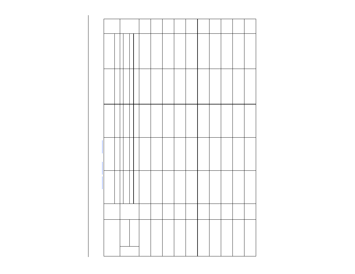
AC CHARACTERISTICS
(V
CC
= 4.5V to 5.5V; T
A
= -40�C to +85�C)* (
Figure 1
,
Figure 2
, and
Figure 3
)
1 CYCLE
PAGE MODE 1
2 CYCLE
PAGE MODE 1
4 CYCLE
PAGE MODE 1
PAGE MODE 2
NON-PAGE MODE
PARAMETER SYMBOL
MIN MAX MIN MAX MIN MAX MIN MAX MIN MAX
UNITS
0 25 0 25 0 25 0 25 0 25
External Oscillator
(25MHz, 33MHz)
0 33 0 33 0 33 0 33 0 33
1 25 1 25 1 25 1 25 1 25
S
ystem
Cloc
k
(N
ot
e 1
)
External Crystal
(25MHz, 33MHz)
1 / t
CLCL
1 33 1 33 1 33 1 33 1 33
MHz
ALE Pulse Width (Note 2)
t
LHLL
0.5t
CLCL
- 2
+ t
STC3
t
CLCL
- 2 +
t
STC3
2t
CLCL
- 4 +
t
STC3
1.5t
CLCL
- 5 +
t
STC3
1.5t
CLCL
- 5 +
t
STC3
ns
Port 0 Instruction Address
Valid to ALE Low
t
AVLL
t
CLCL
- 2
0.5t
CLCL
- 2
ns
Port 2 Instruction Address
Valid to ALE Low
t
AVLL2
0.5t
CLCL
- 4
0.5t
CLCL
- 4
1.5t
CLCL
- 5
0.5t
CLCL
- 2
t
CLCL
- 2
ns
Port 0 Data AddressValid to
ALE Low
t
AVLL3
t
CLCL
- 2 +
t
STC3
0.5t
CLCL
- 2 +
t
STC3
ns
Program Address Hold
After ALE Low
t
LLAX
0.5t
CLCL
- 8
1.5t
CLCL
- 8
2.5t
CLCL
- 8
0.5t
CLCL
- 8
0.5t
CLCL
- 8
ns
Address Hold After ALE
Low MOVX Write
t
LLAX2
0.5t
CLCL
- 8
+ t
STC4
1.5t
CLCL
- 8
+ t
STC4
2.5t
CLCL
- 8
+ t
STC4
0.5t
CLCL
- 8 +
t
STC4
0.5t
CLCL
- 8 +
t
STC4
ns
Address Hold After ALE
Low MOVX Read
t
LLAX3
0.5t
CLCL
- 8
+ t
STC4
1.5t
CLCL
- 8
+ t
STC4
2.5t
CLCL
- 8
+ t
STC4
0.5t
CLCL
- 8 +
t
STC4
0.5t
CLCL
- 8 +
t
STC4
ns
ALE Low to Valid
Instruction In
t
LLIV
2.5t
CLCL
-
20
2.5t
CLCL
-
20
ns
ALE Low to
PSEN Low
t
LLPL
1.5t
CLCL
- 6
0.5t
CLCL
- 6
ns
PSEN Pulse Width for
Program Fetch
t
PLPH
t
CLCL
- 5
t
CLCL
- 5
2t
CLCL
- 5
t
CLCL
- 5
2t
CLCL
- 5
ns

DS89C420 Ultra-High-Speed Microcontroller
5 of 47
1 CYCLE
PAGE MODE 1
2 CYCLE
PAGE MODE 1
4 CYCLE
PAGE MODE 1
PAGE MODE 2
NON-PAGE MODE
PARAMETER SYMBOL
MIN MAX MIN MAX MIN MAX MIN MAX MIN MAX
UNITS
PSEN Low to Valid
Instruction In
t
PLIV
t
CLCL
- 18
t
CLCL
- 18
2t
CLCL
- 18
t
CLCL
- 18
2t
CLCL
- 18
ns
Input Instruction Hold After
PSEN
t
PXIX
0 0 0 0 0
ns
Input Instruction Float After
PSEN
t
PXIZ
t
CLCL
- 5
t
CLCL
- 5
ns
Port 0 Address to Valid
Instruction In
t
AVIV0
1.5t
CLCL
-
20
3t
CLCL
- 20
ns
Port 2 Address to Valid
Instruction In
t
AVIV2
t
CLCL
- 18
1.5t
CLCL
-
18
2.5t
CLCL
-
18
3t
CLCL
- 20
3.5t
CLCL
-
20
ns
PSEN Low to Port 0
Address Float
t
PLAZ
0 0
ns
RD Pulse Width (P3.7)
(Note 2)
t
RLRH
t
CLCL
- 5 +
t
STC1
t
CLCL
- 5 +
t
STC1
2t
CLCL
- 5 +
t
STC1
2t
CLCL
- 5 +
t
STC1
2t
CLCL
- 5 +
t
STC1
ns
WR Pulse Width (P3.6)
(Note 2)
t
WLWH
t
CLCL
- 5 +
t
STC1
t
CLCL
- 5 +
t
STC1
2t
CLCL
- 5 +
t
STC1
2t
CLCL
- 5 +
t
STC1
2t
CLCL
- 5 +
t
STC1
ns
RD (P3.7) Low to Valid
Data In (Note 2)
t
RLDV
t
CLCL
- 15 +
t
STC1
t
CLCL
- 15 +
t
STC1
2t
CLCL
- 15
+ t
STC1
2t
CLCL
- 15
+ t
STC1
2t
CLCL
- 15
+ t
STC1
ns
Data Hold After
RD (P3.7)
t
RHDX
0 0 0 0 0
ns
Data Float After
RD (P3.7)
t
RHDZ
t
CLCL
- 5
t
CLCL
- 5
ns
MOVX ALE Low to Input
Data Valid (Note 2)
t
LLDV
2.5t
CLCL
-
20 + t
STC1
2.5t
CLCL
-
20 + t
STC1
ns
Port 0 Address to Valid
Data In (Note 2)
t
AVDV0
3t
CLCL
- 20
+ t
STC1
3t
CLCL
- 20
+ t
STC1
ns