
SCOPE: SWITCHED-CAPACITOR VOLTAGE CONVERTER
Device Type Generic Number SMD Number
01
ICL7660AM(x)/883B 5962-3870702
Case Outline(s). The case outlines shall be designated in Mil-Std-1835 and as follows:
Outline Letter Mil-Std-1835 Case Outline Package Code
SMD MAXIM
GC TV MACY1-X8 8 LEAD CAN TO99
PA JA GDIP1-T8 or CDIP2-T8 8 LEAD CERDIP J8
Absolute Maximum Ratings
Supply Voltage (V
+
to GND, or GND to V
OUT
) .............................................................. 10.5V
Input Voltage on N.C. Boost, LV, OSC 1/............................................ -0.3V
V
IN
(V
+
+0.3V)
LV Input Current 1/.......................................................................................................... 20
µ
A
Output Short-Circuit Duration (V
+
5.5V) ............................................................. Continuous
Lead Temperature (soldering, 10 seconds) ....................................................................... +300
∞
C
Storage Temperature .......................................................................................... -65
∞
C to +150
∞
C
Continuous Power Dissipation ................................................................................... T
A
=
+
70
∞
C
8 lead CERDIP(derate 8.0mW/
∞
C above +70
∞
C) ........................................................... 640mW
8 lead CAN (derate 6.7mW/
∞
C above +70
∞
C) ............................................................... 533mW
Junction Temperature T
J
.............................................................................................. +150
∞
C
Thermal Resistance, Junction to Case,
JC:
Case Outline 8 lead CERDIP........................................................................... 55
∞
C/W
Case Outline 8 lead CAN............................................................................... 45
∞
C/W
Thermal Resistance, Junction to Ambient,
JA:
Case Outline 8 lead CERDIP......................................................................... 125
∞
C/W
Case Outline 8 lead CAN .............................................................................. 150
∞
C/W
Recommended Operating Conditions.
Ambient Operating Range (T
A
) ..................................................................... -55
∞
C to
+
125
∞
C
NOTE 1: Connecting any input terminal to voltages greater than V+ or less than ground may cause latchup.
Do not apply any inputs from sources operating from external supplies before device power-up.
Stresses beyond those listed under "Absolute Maximum Ratings" may cause permanent damage to the device.
These are stress ratings only, and functional operation of the device at these or any other conditions beyond
those indicated in the operational sections of the specifications is not implied. Exposure to absolute maximum
rating conditions for extended periods may affect device reliability.
----------------------------
Electrical Characteristics of ICL7660AMxx/883B
19-0161
Rev. D
for /883B and SMD 5962-3870702
Page 2 of
5
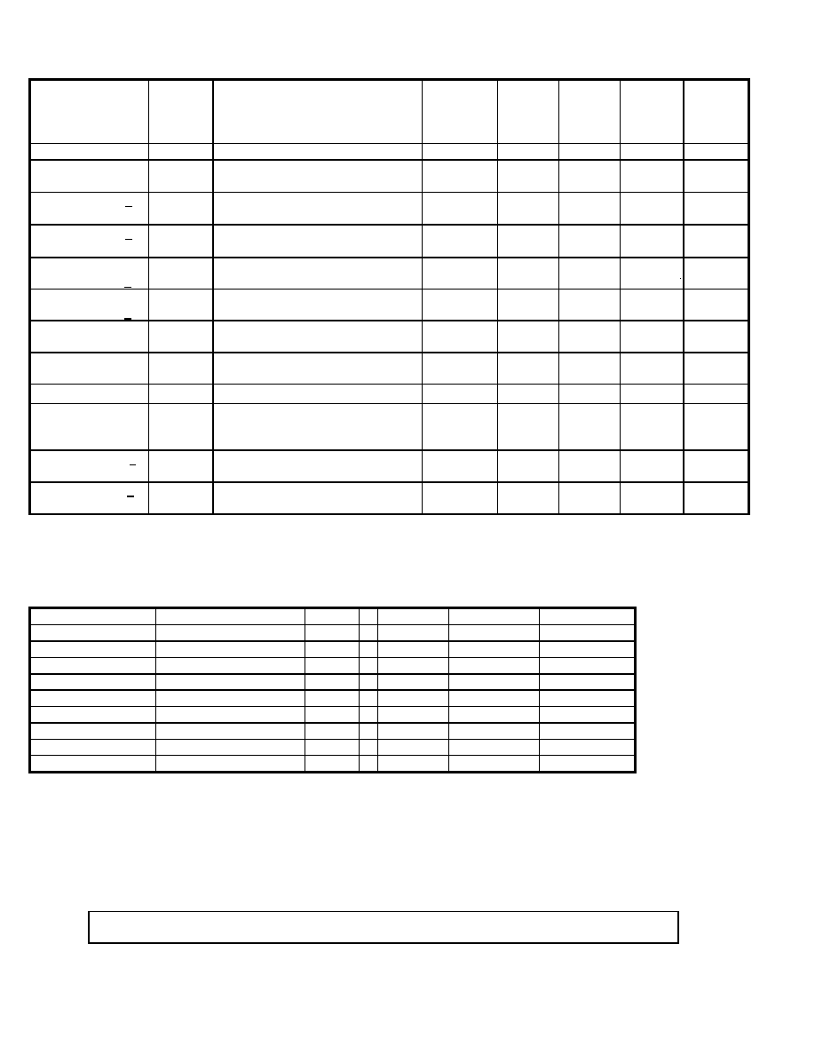
TABLE 1. ELECTRICAL TESTS
TEST
Symbol
CONDITIONS
-55
∞
C <=T
A
<= +125
∞
C
V
+
=+5.0V, LV pin=0V,I
LOAD
=0mA
Unless otherwise specified
Group A
Subgroup
Device
type
Limits
Min
Limits
Max
Units
SWITCH
Supply Current
I+
RL=
, Boost and OSC = no
connection, LV open
1
2,3
All
175
250
µ
A
Supply Current 2/
I+
RL=
, Boost and OSC = no
connection, LV open, V
+
=10.5V
1
2,3
All
3.5
2.0
5.5
7.5
mA
Supply Current 2/
I+
RL=
, Boost and OSC = no
connection, LV open, V
+
=10V
1
2,3
All
3.0
2.0
5.0
7.0
mA
Supply Voltage
Range 3/
V+
RL=10k
, LV open
1,2,3
All
3.0
10.0 V
Supply Voltage
Range 3/
V+
RL=10k
, LV to GND
1,2,3
All
1.5
3.5 V
Output Resistance
R
OUT
I
L
=20mA, f
OSC
=5kHz, LV open
1
2,3
All
100
150
Output Resistance
R
OUT
I
L
=3mA, f
OSC
=2.7kHz, LV to GND
V+=2V
1
2,3
All
250
400
Power Efficiency
P
EFF
R
L
=5k
, f
OSC
=5kHz, LV open
1
All
95
%
Voltage
Conversion
Efficiency
VC
EFF
RL=
, LV open
1
All
99
%
Output Voltage 2/
V
OUT
V+=10V
1
2,3
All
-9.4
-9.0
-10
-10
V
LV pin Voltage 2/
V
LV
V+=10V
1
2,3
All
4.0
3.0
7.0
8.0
V
NOTE 2: Guaranteed if not tested to the limits in Table 1.
NOTE 3: ICL7660 can operate without an external output diode over the full temperature and voltage ranges.
It can also be used with the external diode DX when replacing the Intersil ICL7660. Tests performed
with DX out of circuit.
ORDERING
INFORMATION:
Terminal
ICL7660
ICL7660
SMD #
Maxim #
Pkg.
Number
J8
TO99
5962-3870702MPA
ICL7660AMJA/883B
J8
1
(NC) BOOST
(NC) BOOST
5962-3870702MGC
ICL7660AMTV/883B
TO99
2
CAP+
CAP+
3
GND
GND
4
CAP-
CAP-
5
VOUT
VOUT
6
LV
LV
7
OSC
OSC
8
V+
V+ and Case
----------------------------
Electrical Characteristics of ICL7660AMxx/883B
19-0161
Rev. D
for /883B and SMD 5962-3870702
Page 3 of
5

QUALITY ASSURANCE
Sampling and inspection procedures shall be in accordance with MIL-Prf-38535, Appendix A as specified in Mil-
Std-883.
Screening shall be in accordance with Method 5004 of Mil-Std-883. Burn-in test Method 1015:
1. Test Condition, A, B, C, or D.
2. TA = +125
∞
C minimum.
3. Interim and final electrical test requirements shall be specified in Table 2.
Quality conformance inspection shall be in accordance with Method 5005 of Mil-Std-883, including Groups A, B,
C, and D inspection.
Group A inspection:
1. Tests as specified in Table 2.
2. Selected subgroups in Table 1, Method 5005 of Mil-Std-883 shall be omitted.
Group C and D inspections:
a. End-point electrical parameters shall be specified in Table 1.
b. Steady-state life test, Method 1005 of Mil-Std-883:
1. Test condition A, B, C, D.
2. TA = +125
∞
C, minimum.
3. Test duration, 1000 hours, except as permitted by Method 1005 of Mil-Std-883.
TABLE 2. ELECTRICAL TEST REQUIREMENTS
Mil-Std-883 Test Requirements
Subgroups
per Method 5005, Table 1
Interim Electric Parameters
Method 5004
1
Final Electrical Parameters
Method 5005
1*, 2, 3
Group A Test Requirements
Method 5005
1, 2, 3
Group C and D End-Point Electrical Parameters
Method 5005
1
* PDA applies to Subgroup 1 only.
----------------------------
Electrical Characteristics of ICL7660AMxx/883B
19-0161
Rev. D
for /883B and SMD 5962-3870702
Page 4 of
5