 | –≠–ª–µ–∫—Ç—Ä–æ–Ω–Ω—ã–π –∫–æ–º–ø–æ–Ω–µ–Ω—Ç: ICL7665AC | –°–∫–∞—á–∞—Ç—å:  PDF PDF  ZIP ZIP |
_______________General Description
The ICL7665 warns microprocessors (
µ
Ps) of overvolt-
age and undervoltage conditions. It draws a typical
operating current of only 3µA. The trip points and hys-
teresis of the two voltage detectors are individually pro-
grammed via external resistors to any voltage greater
than 1.3V. The ICL7665 will operate from any supply
voltage in the 1.6V to 16V range, while monitoring volt-
ages from 1.3V to several hundred volts. The Maxim
ICL7665A is an improved version with a 2%-accurate
V
SET1
threshold and guaranteed performance over
temperature.
The 3µA quiescent current of the ICL7665 makes it
ideal for voltage monitoring in battery-powered sys-
tems. In both battery- and line-powered systems, the
unique combination of a reference, two comparators,
and hysteresis outputs reduces the size and compo-
nent count of many circuits.
________________________Applications
µP Voltage Monitoring
Low-Battery Detection
Power-Fail and Brownout Detection
Battery Backup Switching
Power-Supply Fault Monitoring
Over/Undervoltage Protection
High/Low Temperature, Pressure, Voltage Alarms
____________________________Features
o
µP Over/Undervoltage Warning
o
Improved Second Source
o
Dual Comparator with Precision Internal Reference
o
3µA Operating Current
o
2% Threshold Accuracy (ICL7665A)
o
1.6V to 16V Supply Voltage Range
o
On-Board Hysteresis Outputs
o
Externally Programmable Trip Points
o
Monolithic, Low-Power CMOS Design
______________Ordering Information
Ordering Information continued on last page.
ICL7665
Microprocessor Voltage Monitor with
Dual Over/Undervoltage Detection
________________________________________________________________
Maxim Integrated Products
1
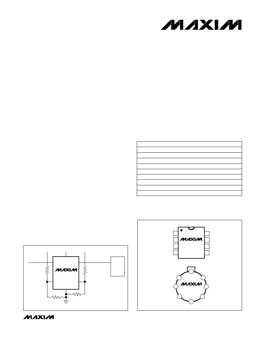
1
2
3
4
8
7
6
5
OUT2
SET2
HYST2
GND
SET1
HYST1
OUT1
ICL7665
DIP/SO
TOP VIEW
2
8
4
6
1
7
3
5
ICL7665
V+ (CASE)
HYST2
SET2
OUT2
OUT1
HYST1
SET1
TO-99
GND
V+
_________________Pin Configurations
ICL7665
OUT1
OUT2
SET2
SET1
V+
V
IN2
V
IN1
V+
8
4
1
7
6
3
GND
OVERVOLTAGE
DETECTION
UNDERVOLTAGE
DETECTION
SIMPLE THRESHOLD DETECTOR
NMI
__________Typical Operating Circuit
19-0001; Rev 2; 8/97
PART
TEMP. RANGE
PIN-PACKAGE
ICL7665CPA
0∞C to +70∞C
8 Plastic DIP
ICL7665ACPA
0∞C to +70∞C
8 Plastic DIP
ICL7665BCPA
0∞C to +70∞C
8 Plastic DIP
ICL7665CSA
0∞C to +70∞C
8 SO
ICL7665ACSA
0∞C to +70∞C
8 SO
ICL7665BCSA
0∞C to +70∞C
8 SO
ICL7665CJA
0∞C to +70∞C
8 CERDIP
ICL7665ACJA
0∞C to +70∞C
8 CERDIP
ICL7665BCJA
0∞C to +70∞C
8 CERDIP
For free samples & the latest literature: http://www.maxim-ic.com, or phone 1-800-998-8800.
For small orders, phone 408-737-7600 ext. 3468.
ICL7665
Microprocessor Voltage Monitor with
Dual Over/Undervoltage Detection
2
_______________________________________________________________________________________
ABSOLUTE MAXIMUM RATINGS
ELECTRICAL CHARACTERISTICS
(V+ = 5V, T
A
= +25∞C, unless otherwise noted.)
Stresses beyond those listed under "Absolute Maximum Ratings" may cause permanent damage to the device. These are stress ratings only, and functional
operation of the device at these or any other conditions beyond those indicated in the operational sections of the specifications is not implied. Exposure to
absolute maximum rating conditions for extended periods may affect device reliability.
Note 1:
Due to the SCR structure inherent in the CMOS process used to fabricate these devices, connecting any terminal to volt-
ages greater than (V+ + 0.3V) or less than (GND - 0.3V) may cause destructive latchup. For this reason, we recommend
that inputs from external sources that are not operating from the same power supply
not
be applied to the device before its
supply is established, and that in multiple supply systems, the supply to the ICL7665 be turned on first. If this is not possi-
ble, currents into inputs and/or outputs must be limited to ±0.5mA and voltages must not exceed those defined above.
Supply Voltage (Note 1) .........................................-0.3V to +18V
Output Voltages OUT1 and OUT2
(with respect to GND) (Note 1) ..........................-0.3V to +18V
Output Voltages HYST1 and HYST2
(with respect to V+) (Note 1) .............................+0.3V to -18V
Input Voltages SET1 and SET2
(Note 1)........................................(GND - 0.3V) to (V+ + 0.3V)
Maximum Sink Output Current
OUT1 and OUT2.............................................................25mA
Maximum Source Output Current
HYST1 and HYST2 ........................................................-25mA
Continuous Power Dissipation (T
A
= +70∞C)
Plastic DIP (derate 9.09mW/∞C above +70∞C) ............727mW
SO (derate 5.88mW/∞C above +70∞C) ........................471mW
CERDIP (derate 8.00mW/∞C above +70∞C) ................640mW
TO-99 (derate 6.67mW/∞C above +70∞C) ...................533mW
Operating Temperature Ranges
ICL7665C_ _.......................................................0∞C to +70∞C
ICL7665I_ _ .....................................................-20∞C to +85∞C
ICL7665E_ _ ....................................................-40∞C to +85∞C
Storage Temperature Range .............................-65∞C to +160∞C
Lead Temperature (soldering, 10sec) .............................+300∞C
PARAMETER
SYMBOL
CONDITIONS
MIN
TYP
MAX
UNITS
Operating Supply Voltage
V+
ICL7665
T
A
= +25∞C
1.6
16
V
T
A
= T
MIN
to T
MIN
1.8
16
ICL7665A
T
A
= T
MIN
to T
MIN
2.0
16
ICL7665B
T
A
= +25∞C
1.6
10
Input Trip Voltage
V
SET
ICL7665, ICL7665B, T
A
= +25∞C
V
SET1
1.150
1.300
1.450
V
V
SET2
1.200
1.300
1.400
ICL7665A, T
A
= +25∞C
V
SET1
1.275
1.300
1.325
V
SET2
1.225
1.300
1.375
ICL7665A, T
A
= T
MIN
to T
MAX
V
SET1
1.250
1.300
1.350
V
SET2
1.215
1.300
1.385
V
SET
Tempco
100
ppm/∞C
R
OUT1
, R
OUT2
, R
HYST1
, R
HYST2
= 1M
0.004
%/V
Supply Current
I+
GND
V
SET1,
V
SET2
V+,
all outputs open
circuit
V+ = 2V
2.5
10
µ
A
V+ = 9V
2.6
10
V+ = 15V
2.9
15
ICL7665B,
T
A
= +25∞C
V+ = 2V
2.5
10
V+ = 9V
2.6
10
T
A
= T
MIN
to T
MIN
1.8
10
ICL7665,
T
A
= +25∞C;
ICL7665A,
T
A
= T
MIN
to T
MAX
Supply Voltage Sensitivity
of V
SET1
, V
SET2
ICL7665
Microprocessor Voltage Monitor with
Dual Over/Undervoltage Detection
_______________________________________________________________________________________
3
ELECTRICAL CHARACTERISTICS (continued)
(V+ = 5V, T
A
= +25∞C, unless otherwise noted.)
PARAMETER
CONDITIONS
MIN
TYP
MAX
UNITS
Output Leakage Current
I
OLK
,
I
HLK
All grades, V
SET
= 0V or
V
SET
2V, T
A
= +25∞C
OUT1, OUT2
10
200
nA
HYST1, HSYT2
-10
-100
OUT1, OUT2
2000
HYST1, HSYT2
-500
ICL7665B, V+ = 9V,
T
A
= T
MIN
to T
MAX
OUT1, OUT2
2000
HYST1, HSYT2
-500
V
OUT1
Saturation
Voltage
V
SET1
= 2V,
I
OUT1
= 2mA
ICL7665, ICL7665B: V+ = 2V
0.20
0.50
ICL7665A: V+ = 2V
0.20
All grades: V+ = 5V
0.10
0.30
ICL7665, ICL7665A: V+ = 15V
0.06
0.20
ICL7665B: V+ = 9V
0.06
0.25
All grades: V+ = 2V
-0.15
-0.30
All grades: V+ = 5V
-0.05
-0.15
ICL7665, ICL665A: V+ = 15V
-0.02
-0.10
ICL7665B: V+ = 9V
-0.02
-0.15
V
OUT2
Saturation
Voltage
V
SET2
= 0V,
I
OUT2
= 2mA
All grades: V+ = 2V
0.20
0.50
V
All grades: V+ = 5V
0.15
0.30
ICL7665, ICL665A: V+ = 15V
0.11
0.25
ICL7665B: V+ = 9V
0.11
0.30
V
HYST2
Saturation
Voltage
All grades: V+ = 2V
-0.25
-0.80
V
All grades: V+ = 5V
-0.43
-1.00
ICL7665: V+ = 15V
-0.35
-0.80
ICL7665A: V+ = 15V
-0.35
-1.00
ICL7665B: V+ = 9V
-0.35
-1.00
I
SET
GND
V
SET
V+
±0.01
±10
nA
V
SET
0.1
mV
V
SET1
≠
V
SET2
±5
±50
mV
±0.1
mV
SYMBOL
V
V
HYST1
Saturation
Voltage
V
V
SET1
= 2V,
I
HYST1
= -0.5mA
ICL7665, ICL7665A,
V+ = 15V,
T
A
= T
MIN
to T
MAX
V
SET2
= 2V,
I
HYST2
= -0.2mA
V
SET2
= 2V,
I
HYST2
= -0.5mA
V
SET
Input Leakage
Current
R
OUT
, R
HYST
= 1M
R
OUT
, R
HYST
= 1M
R
OUT
= 4.7k
, R
HYST
= 20k
,
V
OUT
LO = 1% V+, V
OUT
HI = 99% V+
V
SET
Input Change for
Complete Output
Change
Difference in Trip
Voltage
Output/Hysteresis
Difference
ICL7665
Microprocessor Voltage Monitor with
Dual Over/Undervoltage Detection
4
_______________________________________________________________________________________
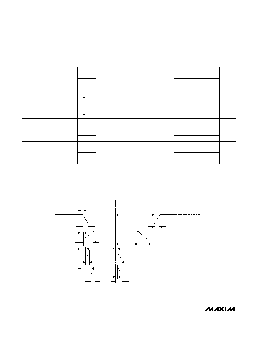
AC OPERATING CHARACTERISTICS
(V+ = 5V, T
A
= +25∞C, unless otherwise noted.)
V
SET
switched between 1.0V and 1.6V,
R
OUT
= 4.7k
, C
L
= 12pF,
R
HYST
= 20k
µs
1.8
t
H2f
Output Fall Times
4.0
t
H1f
0.7
t
O2f
0.6
t
O1f
V
SET
switched between 1.0V and 1.6V,
R
OUT
= 4.7k
, C
L
= 12pF,
R
HYST
= 20k
µs
0.7
t
H2r
Output Rise Times
7.5
t
H1r
0.8
t
O2r
0.6
t
O1r
V
SET
switched from 1.6V to 1.0V,
R
OUT
= 4.7k
, C
L
= 12pF,
R
HYST
= 20k
µs
60
t
SH2d
Output Delay Time,
Input Going Low
60
t
SO2d
80
t
SH1d
75
t
SO1d
V
SET
switched from 1.0V to 1.6V,
R
OUT
= 4.7k
, C
L
= 12pF,
R
HYST
= 20k
CONDITIONS
µs
55
t
SH2d
Output Delay Time,
Input Going High
55
t
SO2d
90
t
SH1d
85
t
SO1d
UNITS
MIN
TYP
MAX
SYMBOL
PARAMETER
INPUT
OUT1
HYST1
OUT2
HYST2
t
O1f
t
SO1d
t
H1r
t
SO2d
t
SH2d
t
O2r
t
O2f
t
SH2d
t
O1r
1.6V
1.0V
V+ (5V)
GND
V+ (5V)
GND
V+ (5V)
GND
V+ (5V)
GND
V
SET1,
V
SET2
t
SH1d
t
H2r
t
H2f
t
SO2d
t
SH1d
t
H1f
t
SO1d
_______________________________________________________Switching Waveforms
ICL7665
Microprocessor Voltage Monitor with
Dual Over/Undervoltage Detection
_______________________________________________________________________________________
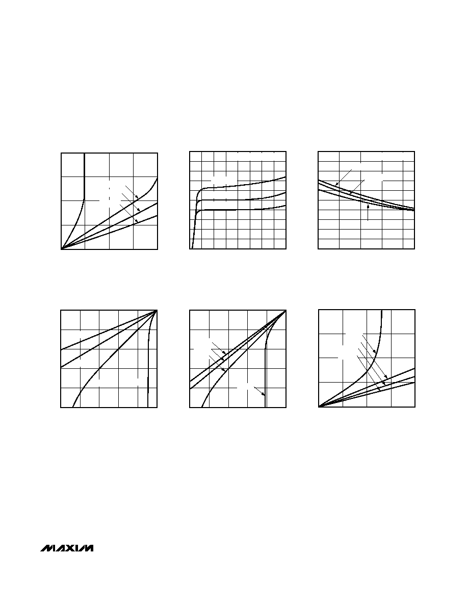
5
2.0
0
0
15
OUT1 SATURATION VOLTAGE AS A
FUNCTION OF OUTPUT CURRENT
0.5
1.5
ICL7665-01
I
OUT
OUT1 (mA)
VOLTAGE SATURATION (V)
1.0
10
5
20
V+ = 2V
V+ = 9V
V+ = 15V
V+ = 5V
SUPPLY CURRENT AS A
FUNCTION OF SUPPLY VOLTAGE
SUPPLY CURRENT (
µ
A)
0
0
SUPPLY VOLTAGE (V)
ICL7665-02
2
4
6
8
10
12
14
16
0.5
1.0
T
A
= +25∞C
T
A
= +70∞C
0V
V
SET1
, V
SET2
V+
1.5
2.0
2.5
3.0
3.5
5.0
4.5
4.0
T
A
= -20∞C
SUPPLY CURRENT AS A
FUNCTION OF AMBIENT TEMPERATURE
-20
0
20
40
60
AMBIENT TEMPERATURE (∞C)
ICL7665-03
SUPPLY CURRENT (
µ
A)
0
0.5
1.5
2.0
2.5
3.0
3.5
4.0
5.0
1.0
4.5
V+ = 15V
V+ = 9V
V+ = 2V
0V
V
SET1
, V
SET2
V+
-2.0
-1.6
-1.2
-0.8
-0.4
0
-20
-16
-12
-8
-4
0
HYST1 OUTPUT SATURATION VOLTAGE
vs. HYST1 OUTPUT CURRENT
HYST1 OUTPUT SATURATION VOLTAGE (V)
HYST1 OUTPUT CURRENT (mA)
ICL7665-04
V+ = 2V
V+ = 5V
V+ = 9V
V+ = 15V
-5
-4
-3
-2
-1
0
-5
-4
-3
-2
-1
0
HYST2 OUTPUT SATURATION VOLTAGE
vs. HYST2 OUTPUT CURRENT
HYST2 OUTPUT SATURATION VOLTAGE (V)
HYST2 OUTPUT CURRENT (mA)
ICL7665-05
V+ = 2V
V+ = 15V
V+ = 9V
V+ = 5V
2.0
1.5
1.0
0.5
0
20
15
10
5
0
OUT2 SATURATION VOLTAGE AS A
FUNCTION OF OUTPUT CURRENT
VOLTAGE SATURATION (V)
I
OUT
OUT2 (mA)
ICL7665-06
V+ = 2V
V+ = 5V
V+ = 9V
V+ = 15V
__________________________________________Typical Operating Characteristics
(T
A
= +25∞C, unless otherwise noted.)
ICL7665
_______________Detailed Description
As shown in the block diagram of Figure 2, the Maxim
ICL7665 combines a 1.3V reference with two com-
parators, two open-drain N-channel outputs, and two
open-drain P-channel hysteresis outputs. The refer-
ence and comparator are very low-power linear CMOS
circuits, with a total operating current of 10
µ
A maxi-
mum, 3
µ
A typical. The N-channel outputs can sink
greater than 10mA, but are unable to source any cur-
rent. These outputs are suitable for wire-OR connections
and are capable of driving TTL inputs when an external
pull-up resistor is added.
The ICL7665 Truth Table is shown in Table 1. OUT1 is
an inverting output; all other outputs are noninverting.
HYST1 and HYST2 are P-channel current sources
whose sources are connected to V+. OUT1 and OUT2
are N-channel current sinks with their sources connect-
ed to ground. Both OUT1 and OUT2 can drive at least
one TTL load with a V
OL
of 0.4V.
In spite of the very low operating current, the ICL7665
has a typical propagation delay of only 75
µ
s. Since the
comparator input bias current and the output leakages
are very low, high-impedance external resistors can be
used. This design feature minimizes both the total sup-
ply current used and loading on the voltage source that
is being monitored.
Microprocessor Voltage Monitor with
Dual Over/Undervoltage Detection
6
_______________________________________________________________________________________
Figure 1. Test Circuit
HYST2 = OFF = LOW
OUT2 = ON = LOW
V
SET2
< 1.3V
HYST2 = ON = HI
OUT2 = OFF = HI
V
SET2
> 1.3V
HYST1 = OFF = LOW
OUT1 = OFF = HI
V
SET1
< 1.3V
HYST1 = ON = HI
OUT1 = ON = LOW
V
SET1
> 1.3V
HYSTERESIS
OUTPUT
INPUT*
Table 1. ICL7665 Truth Table
V+
HYST1
HYST2
OUT1
OUT2
TO V+
SET2
SET1
1.3V
BANDGAP
REFERENCE
Figure 2. Block Diagram
1
2
3
4
8
7
6
5
ICL7665
OUT1
HYST1
SET1
GND
V+
OUT2
SET2
HSYT2
12pF
12pF
12pF
12pF
OUT1
HYST1
OUT2
HSYT2
4.7k
4.7k
V+
1.6V
1.0V
INPUT
20k
20k
* See Electrical Characteristics
OUT1 is an inverting output; all others are noninverting. OUT1
and OUT2 are open-drain, N-channel current sinks. HYST1
and HYST2 are open-drain, P-channel current sinks.
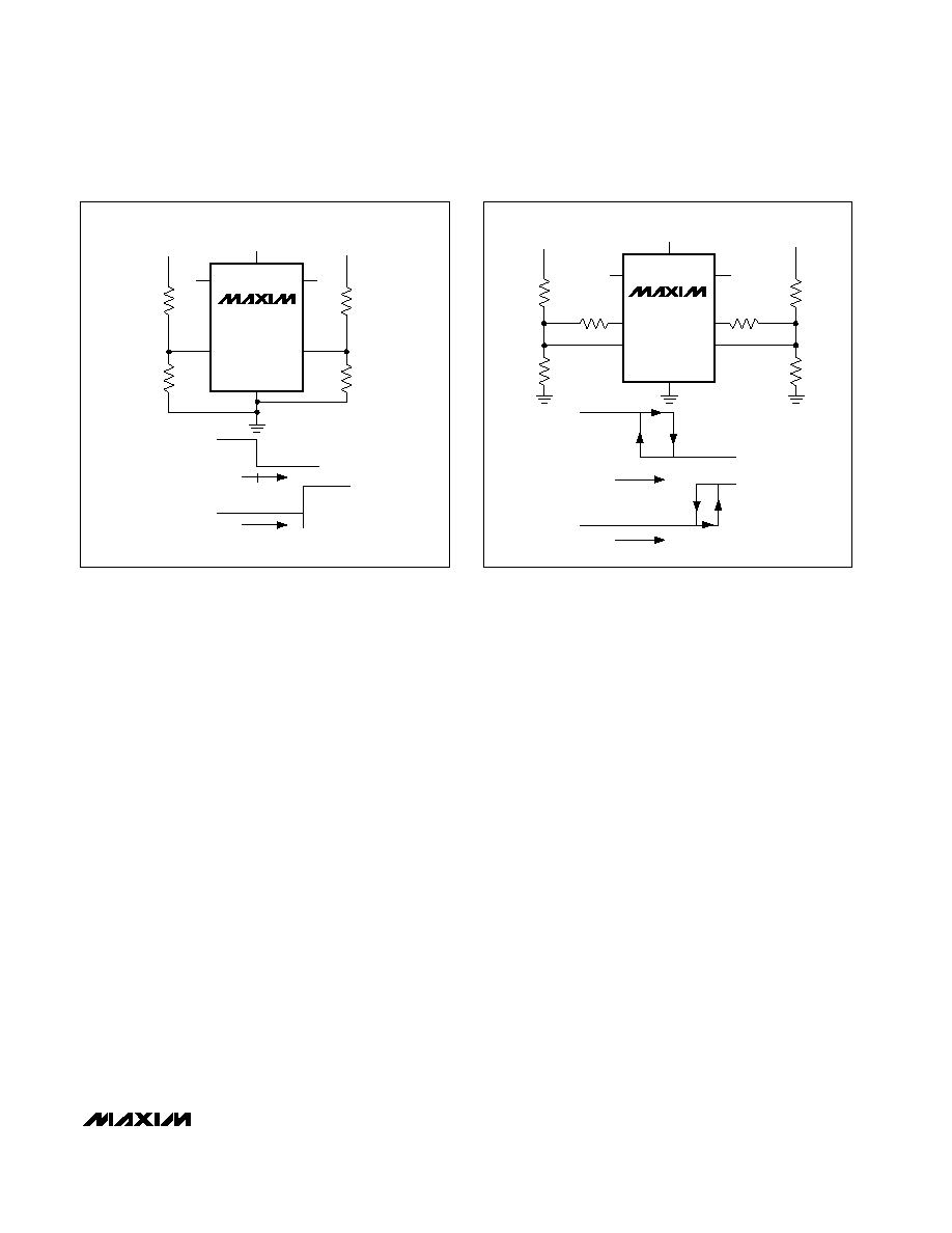
Basic Over/Undervoltage
Detection Circuits
Figures 3, 4, and 5 show the three basic voltage detec-
tion circuits.
The simplest circuit, depicted in Figure 3, does not
have any hysteresis. The comparator trip-point formulas
can easily be derived by observing that the comparator
changes state when the V
SET
input is 1.3V. The exter-
nal resistors form a voltage divider that attenuates the
input signal. This ensures that the V
SET
terminal is at
1.3V when the input voltage is at the desired compara-
tor trip point. Since the bias current of the comparator
is only a fraction of a nanoamp, the current in the volt-
age divider can be less than one microamp without los-
ing accuracy due to bias currents. The ICL7665A has a
2% threshold accuracy at +25∞C, and a typical temper-
ature coefficient of 100ppm/∞C including comparator
offset drift, eliminating the need for external poten-
tiometers in most applications.
Figure 4 adds another resistor to each voltage detector.
This third resistor supplies current from the HYST out-
put whenever the V
SET
input is above the 1.3V thresh-
old. As the formulas show, this hysteresis resistor
affects only the lower trip point. Hysteresis (defined as
the difference between the upper and lower trip points)
keeps noise or small variations in the input signal from
repeatedly switching the output when the input signal
remains near the trip point for a long period of time.
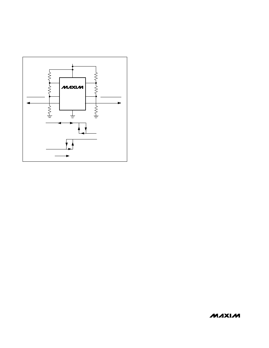
The third basic circuit, Figure 5, is suitable only when the
voltage to be detected is also the power-supply voltage for
the ICL7665. This circuit has the advantage that all of the
current flowing through the input divider resistors flows
through the hysteresis resistor. This allows the use of
higher-value resistors, without hysteresis output leakage
having an appreciable effect on the trip point.
Resistor-Value Calculations
Figure 3
1) Choose a value for R11. This value determines the
amount of current flowing though the input divider,
equal to V
SET
/ R11. R11 can typically be in the
range of 10k
to 10M
.
2) Calculate R21 based on R11 and the desired trip
point:
V
TRIP
≠ V
SET
V
TRIP
≠ 1.3V
R21 = R11
(
--------------
)
= R11
(
------------
)
V
SET
1.3V
ICL7665
Microprocessor Voltage Monitor with
Dual Over/Undervoltage Detection
_______________________________________________________________________________________
7
Figure 3. Simple Threshold Detector
Figure 4. Threshold Detector with Hysteresis
ICL7665
OUT1
OUT2
SET2
SET1
R21
R11
R22
R12
V
IN1
V+
V
IN2
OUT1
V
IN1
V
TRIP1
V
TRIP2
OUT2
V
IN2
ICL7665
OUT1
OUT2
SET2
SET1
R21
R11
R22
R12
V
IN1
V+
V
IN2
HYST1
HYST2
R31
R32
V+
OUT1
V
L1
V
U1
0V
V+
V
U2
OUT2
V
IN1
0V
V
L2
V
IN2
ICL7665
Microprocessor Voltage Monitor with
Dual Over/Undervoltage Detection
8
_______________________________________________________________________________________
Figure 4
1) Choose a resistor value for R11. Typical values are
in the 10k
to 10M
range.
2) Calculate R21 for the desired upper trip point, V
U,
using the formula:
V
U
- V
SET
V
U
≠ 1.3V
R21 = R11
(
------------
)
= R11
(
----------
)
V
SET
1.3V
3) Calculate R31 for the desired amount of hysteresis:
(R21) (V+ ≠ V
SET
)
(R21) (V+ ≠ 1.3V)
R31 = ------------------ = ------------------
V
U
≠ V
L
V
U
≠ V
L
or, if V+ = V
IN
:
(R21) (V
L
≠ V
SET
)
(R21) (V
L
≠ 1.3V)
R31 = ------------------ = ------------------
V
U
≠ V
L
V
U
≠ V
L
4) The trip voltages are not affected by the absolute
value of the resistors, as long as the impedances
are high enough that the resistance of R31 is
much greater than the HYST output's resistance,
and the current through R31 is much higher than
the HYST output's leakage current. Normally, R31
will be in the 100k
to 22M
range. Multiplying or
dividing all three resistors by the same factor will
not affect the trip voltages.
Figure 5
1) Select a value for R11, usually between 10k
and
10M
.
2) Calculate R21:
V
L
≠ V
SET
V
L
≠ 1.3V
R21 = R11
(
------------
)
= R11
(
----------
)
V
SET
1.3
3) Calculate R31:
V
U
≠ V
L
R31 = R11
(
----------
)
V
SET
4) As in the other circuits, all three resistor values may
be scaled up or down in value without changing V
U
and V
L
. V
U
and V
L
depend only on the ratio of the
three resistors, if the absolute values are such that
the hysteresis output resistance and the leakage
currents of the V
SET
input and hysteresis output can
be ignored.
__________Applications Information
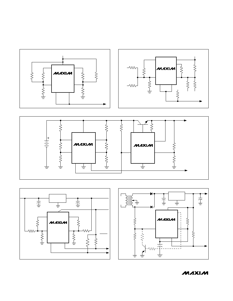
Fault Monitor for a Single Supply
Figure 6 shows a typical over/undervoltage fault monitor
for a single supply. In this case, the upper trip points (con-
trolling OUT1) are centered on 5.5V, with 100mV of hys-
teresis (V
U
= 5.55V, V
L
= 5.45V); and the lower trip points
(controlling OUT2) are centered on 4.5V, also with 100mV
of hysteresis. OUT1 and OUT2 are connected together in
a wire-OR configuration to generate a power-OK signal.
Multiple-Supply Fault Monitor
The ICL7665 can simultaneously monitor several power
supplies, as shown in Figure 7. The easiest way to calculate
the resistor values is to note that when the V
SET
input is at
the trip point (1.3V), the current through R11 is 1.3V / R11.
The sum of the currents through R21A, R21B and R31 must
equal this current when the two input voltages are at the
desired low-voltage detection point. Ordinarily, R21A and
R21B are chosen so that the current through the two resis-
tors is equal. Note that, since the voltage at the ICL7665
V
SET
input depends on the voltage of both supplies being
monitored, there will be some interaction between the low-
voltage trip points for the two supplies. In this example,
OUT1 will go low when either supply is 10% below nominal
(assuming the other supply is at the nominal voltage), or
when both supplies are 5% or more below their nominal
voltage. R31 sets the hysteresis, in this case, to about 43mV
at the 5V supply or 170mV at the 15V supply. The second
section of ICL7665 can be used to detect overvoltage or, as
shown in Figure 7, can be used to detect the absence of
negative supplies. Note that the trip points for OUT2 depend
on both the voltages of the negative power supplies and
the actual voltage of the +5V supply.
Figure 5. Threshold Detector, V
IN
= V+
V
L2
V
U2
ICL7665
OUT1
OUT2
SET2
SET1
R21
R11
V
IN
HYST1
HYST2
OUT1
OUT2
V
IN
V+
GND
OVERVOLTAGE
UNDERVOLTAGE
R31
R32
R22
R12
V
L1
V
U1

ICL7665
Microprocessor Voltage Monitor with
Dual Over/Undervoltage Detection
_______________________________________________________________________________________
9
Combination Low-Battery Warning and
Low-Battery Disconnect
Nickel cadmium (NiCd) batteries are excellent recharge-
able power sources for portable equipment, but care
must be taken to ensure that NiCd batteries are not
damaged by overdischarge. Specifically, a NiCd battery
should not be discharged to the point where the polarity
of the lowest-capacity cell is reversed, and that cell is
reverse charged by the higher-capacity cells. This reverse
charging will dramatically reduce the life of a NiCd battery.
The Figure 8 circuit both prevents reverse charging and
gives a low-battery warning. A typical low-battery warning
voltage is 1V per cell. Since a NiCd "9V" battery is ordi-
narily made up of six cells with a nominal voltage of 7.2V,
a low-battery warning of 6V is appropriate, with a small
hysteresis of 100mV. To prevent overdischarge of a bat-
tery, the load should be disconnected when the battery
voltage is 1V x (N ≠ 1), where N = number of cells. In this
case, the low-battery load disconnect should occur at
5V. Since the battery voltage will rise when the load is
disconnected, 800mV of hysteresis is used to prevent
repeated on/off cycling.
Power-Fail Warning and
Power-Up/Power-Down Reset
Figure 9 illustrates a power-fail warning circuit that
monitors raw DC input voltage to the 7805 three-termi-
nal 5V regulator. The power-fail warning signal goes
high when the unregulated DC input falls below 8.0V.
When the raw DC power source is disconnected or the
AC power fails, the voltage on the input of the 7805
decays at a rate of I
OUT
/ C (in this case, 200mV/ms).
Since the 7805 will continue to provide a 5V output at
1A until V
IN
is less than 7.3V, this circuit will give at
least 3.5ms of warning before the 5V output begins to
drop. If additional warning time is needed, either the
trip voltage or filter capacitance should be increased,
or the output current should be decreased.
The ICL7665 OUT2 is set to trip when the 5V output has
decayed to 3.9V. This output can be used to prevent
the microprocessor from writing spurious data to a
CMOS battery-backup memory, or can be used to acti-
vate a battery-backup system.
AC Power-Fail and Brownout Detector
By monitoring the secondary of the transformer, the cir-
cuit in Figure 10 performs the same power-failure warn-
ing function as Figure 9. With a normal 110V AC input
to the transformer, OUT1 will discharge C1 every
16.7ms when the peak transformer secondary voltage
exceeds 10.2V. When the 110V AC power-line voltage
is either interrupted or reduced so that the peak voltage
is less than 10.2V, C1 will be charged through R1.
OUT2, the power-fail warning output, goes high when
the voltage on C1 reaches 1.3V. The time constant R1 x
C1 determines the delay time before the power-fail warning
signal is activated, in this case 42ms or 2
1
/
2
line cycles.
Optional components R2, R3 and Q1 add hysteresis by
increasing the peak secondary voltage required to dis-
charge C1 once the power-fail warning is active.
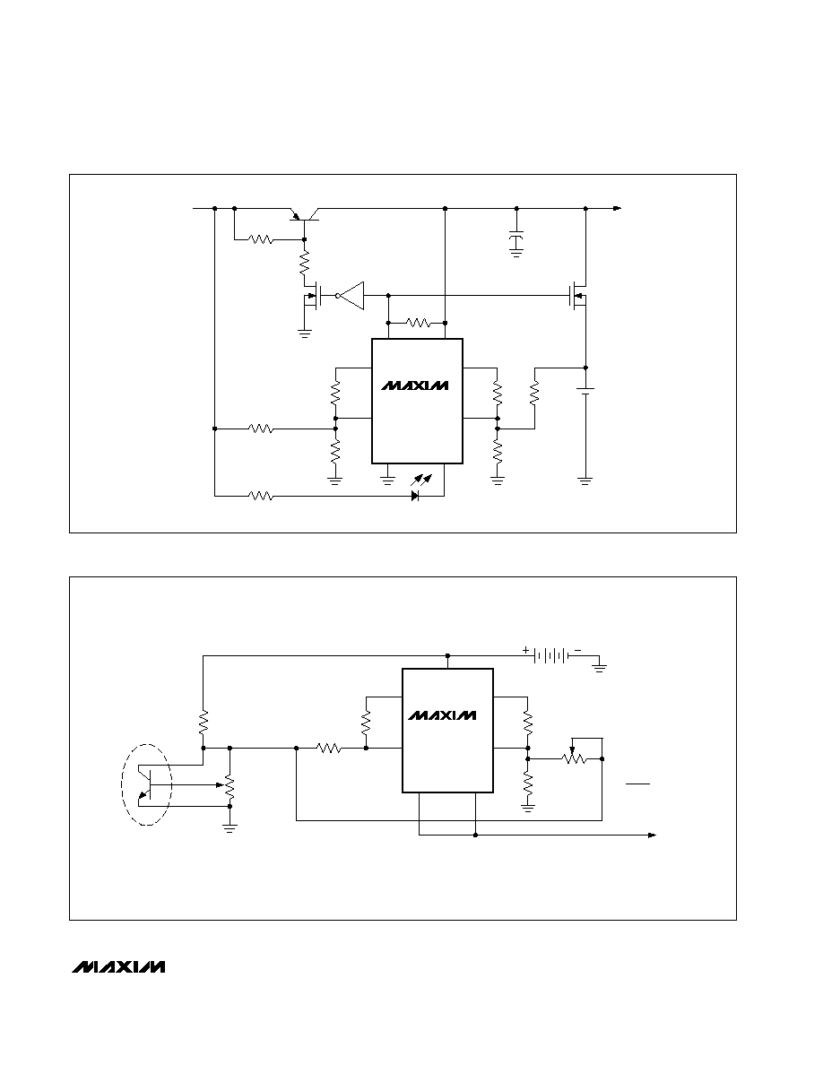
Battery Switchover Circuit
The circuit in Figure 11 performs two functions: switch-
ing the power supply of a CMOS memory to a backup
battery when the line-powered supply is turned off, and
lighting a low-battery-warning LED when the backup
battery is nearly discharged. The PNP transistor, Q1,
connects the line-powered +5V to the CMOS memory
whenever the line-powered +5V supply voltage is
greater than 3.5V. The voltage drop across Q1 will only
be a couple of hundred millivolts, since it will be satu-
rated. Whenever the input voltage falls below 3.5V,
OUT1 goes high, turns off Q1, and connects the 3V
lithium cell to the CMOS memory.
The second voltage detector of the ICL7665 monitors the
voltage of the lithium cell. If the battery voltage falls below
2.6V, OUT2 goes low and the low-battery-warning LED
turns on (assuming that the +5V is present, of course).
Another possible use for the second section of the
ICL7665 is the detection of the input voltage falling
below 4.5V. This signal could then be used to prevent
the microprocessor from writing spurious data to the
CMOS memory while its power-supply voltage is out-
side its guaranteed operating range.
Simple High/Low Temperature Alarm
The circuit in Figure 12 is a simple high/low tempera-
ture alarm, which uses a low-cost NPN transistor as the
sensor and an ICL7665 as the high/low detector. The
NPN transistor and potentiometer R1 form a Vbe multi-
plier whose output voltage is determined by the Vbe of
the transistor and the position of R1's wiper arm. The
voltage at the top of R1 will have a temperature coeffi-
cient of approximately -5mV/∞C. R1 is set so that the
voltage at V
SET2
equals the V
SET2
trip voltage when the
temperature of the NPN transistor reaches the level
selected for the high-temperature alarm. R2 can be
adjusted so that the voltage at V
SET1
is 1.3V when the
NPN transistor's temperature reaches the low-tempera-
ture limit.
ICL7665
Microprocessor Voltage Monitor with
Dual Over/Undervoltage Detection
ICL7665
OUT2
OUT1
SET1
SET2
HYST2
HYST1
R31
22M
22M
100k
POWER OK
301k
R11
49.9k
V+
+5V
-5V
-15V
787k
+5V
+15V
R21A
274k
R21B
1.02M
+5V
HYST1
SET1
HYST2
SET2
GND
OUT2
V+
V+
OUT1
OUT2
SHDN
SENSE
ICL7663
ICL7665
GND
LOW-BATTERY WARNING
LOW-BATTERY SHUTDOWN
+5V, 1A
OUTPUT
R31
OUT1
SET
R21
R11
R32
R22
R12
1M
100
Figure 8. Low-Battery Warning and Low-Battery Disconnect
Figure 7. Multiple-Supply Fault Monitor
HYST1
SET1
HYST2
SET2
ICL7665
V+
UNREGULATED
DC INPUT
BACK-UP
BATTERY
RESET
OR
WRITE
ENABLE
POWER-FAIL WARNING
4700µF
470µF
2.2M
1M
5.6M
715k
130k
22M
OUT2
OUT1
5V, 1A
OUTPUT
7805
5V REGULATOR
HYST1
SET1
HYST2
SET2
OUT1
OUT2
ICL7665
V+
7805
5V REGULATOR
10VAC
60Hz
20V CENTER
TAPPED TRANS
4700
µ
F
R2
1M
681k
Q1
R3
1M
C1
R1
+5V
POWER-FAIL
WARNING
100k
5V, 1A
Figure 9. Power-Fail Warning and Power-Up/Power-Down Reset
Figure 10. AC Power-Fail and Brownout Detector
ICL7665
OUT1
OUT2
SET2
SET1
+5V SUPPLY
HYST1
HYST2
V+
13M
5%
7.5M
5%
249k
324k
100k
100k
OVERVOLTAGE
DETECTOR
V
U
5.55V
V
L
5.45V
UNDERVOLTAGE
DETECTOR
V
U
4.55V
V
L
4.45V
POWER OK
Figure 6. Fault Monitor for a Single Supply
10
______________________________________________________________________________________
ICL7665
Microprocessor Voltage Monitor with
Dual Over/Undervoltage Detection
______________________________________________________________________________________
11
HYST1
SET1
GND
OUT2
SET2
HYST2
OUT1
V+
ICL7665
100k
2N4393
1M
LINE-POWERED
+5V INPUT
Q1
1k
1
µ
F
5.6M
1M
2.4M
220
2N7000
22M
1M
1%
1.15M
1%
3V
LITHIUM
CELL
VCC TO
CMOS
MEMORY
Figure 11. Battery Switchover Circuit
Figure 12. Simple High/Low Temperature Alarm
HYST1
SET1
OUT2
OUT1
SET2
HYST2
V+
ICL7665
R4
22M
R5
27k
R6
22M
R1, 1M
HIGH-
TEMPERATURE
LIMIT
ADJUSTMENT
ALARM
SIGNAL FOR
DRIVING LEDS,
BELLS, ETC.
TEMPERATURE
SENSOR
(GENERAL
PURPOSE NPN
TRANSISTOR)
R7
1.5M
R2
1M
LOW-TEMPERATURE
LIMIT ADJUST
9V
R3
470k
_______________________SCR Latchup
Like all junction-isolated CMOS circuits, the ICL7665 has
an inherent four-layer or SCR structure that can be
triggered into destructive latchup under certain con-
ditions. Avoid destructive latchup by following these
precautions:
1) If either V
SET
terminal can be driven to a voltage
greater than V+ or less than ground, limit the input
current to 500
µ
A maximum. Usually, an input volt-
age divider resistance can be chosen to ensure
the input current remains below 500
µ
A, even
when the input voltage is applied before the
ICL7665 V+ supply is connected.
2) Limit the rate-of-rise of V+ by using a bypass
capacitor near the ICL7665. Rate-of-rise SCRs
rarely occur unless: a) the battery has a low
impedance--as is the case with NiCd and lead
acid batteries; b) the battery is connected directly
to the ICL7665 or is switched on via a mechanical
switch with low resistance; or c) there is little or no
input filter capacitance near the ICL7665. In line-
powered systems, the rate-of-rise is usually limited
by other factors and will not cause a rate-of-rise
SCR action under normal circumstances.
3) Limit the maximum supply voltage (including tran-
sient spikes) to 18V. Likewise, limit the maximum volt-
age on OUT1 and OUT2 to +18V and the maxi-
mum voltage on HYST1 and HYST2 to 18V below V+.
ICL7665
Microprocessor Voltage Monitor with
Dual Over/Undervoltage Detection
PART
TEMP. RANGE
PIN-PACKAGE
ICL7665AC/D
0∞C to +70∞C
Dice*
ICL7665EPA
-40∞C to +85∞C
8 Plastic DIP
ICL7665AEPA
-40∞C to +85∞C
8 Plastic DIP
ICL7665ESA
-40∞C to +85∞C
8 SO
ICL7665AESA
-40∞C to +85∞C
8 SO
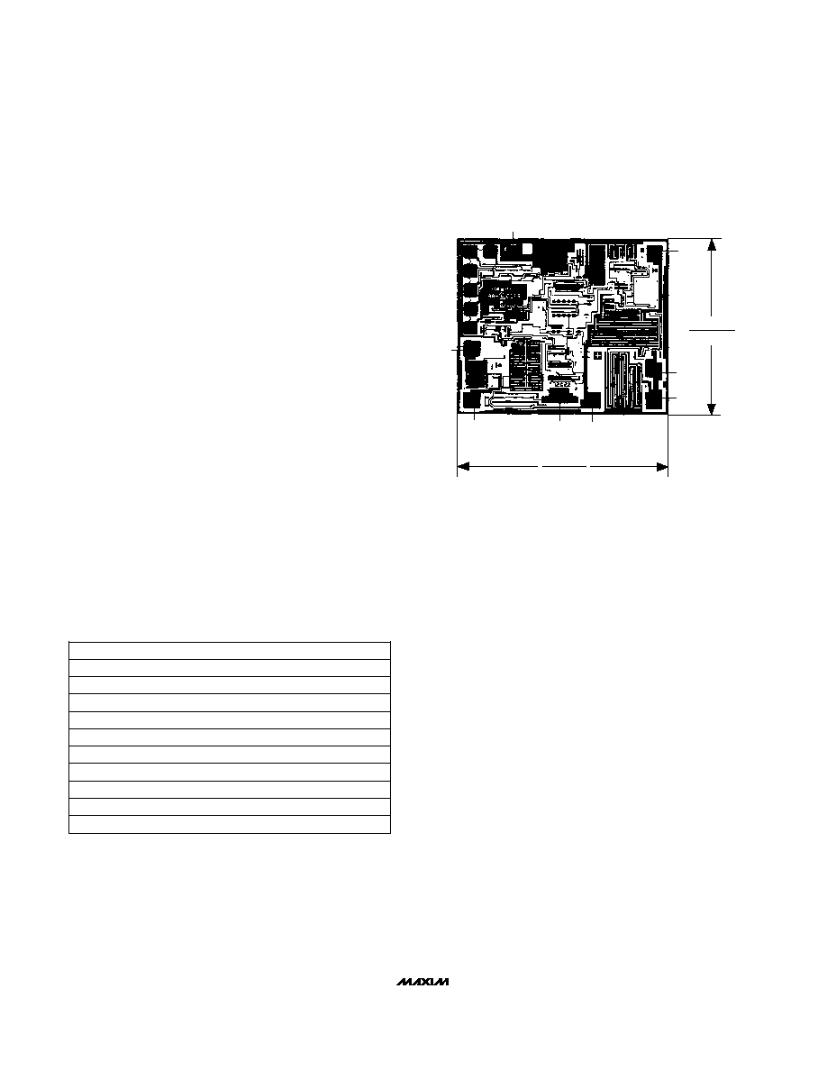
___________________Chip Topography
_Ordering Information (continued)
ICL7665IPA
-20∞C to +85∞C
8 Plastic DIP
ICL7665IJA
-20∞C to +85∞C
8 CERDIP
*Contact factory for dice specifications.
OUT2
V+
HYST1
0.066"
(1.42mm)
0.084"
(1.63mm)
SET1
V-
SET2
HYST2
OUT1
ICL7665CTV
0∞C to +70∞C
8 TO-99
ICL7665ACTV
0∞C to +70∞C
8 TO-99
ICL7665BCTV
0∞C to +70∞C
8 TO-99
TRANSISTOR COUNT: 38
SUBSTRATE CONNECTED TO V+.
Maxim cannot assume responsibility for use of any circuitry other than circuitry entirely embodied in a Maxim product. No circuit patent licenses are
implied. Maxim reserves the right to change the circuitry and specifications without notice at any time.
12
____________________Maxim Integrated Products, 120 San Gabriel Drive, Sunnyvale, CA 94086 408-737-7600
© 1997 Maxim Integrated Products
Printed USA
is a registered trademark of Maxim Integrated Products.