
SCOPE: DUAL-POWER MOSFET DRIVER
Device Type Generic Number SMD Number
01
ICL7667M(x)/883B 5962-87660
Case Outline(s). The case outlines shall be designated in Mil-Std-1835 and as follows:
Outline Letter Mil-Std-1835 Case Outline Package Code
SMD MAXIM
G TV MACY1-X8 8 LEAD CAN TO99
P JA GDIP1-T8 or CDIP2-T8 8 LEAD CERDIP J8
Absolute Maximum Ratings
V
DD
to GND .......................................................................................................................... 18V
Input Voltage ................................................................................ (V
DD
+0.3V) to ( GND
-0.3V)
Lead Temperature (soldering, 10 seconds) ........................................................................... +300
∞
C
Storage Temperature .............................................................................................. -65
∞
C to +150
∞
C
Continuous Power Dissipation ..................................................................................... T
A
=
+
70
∞
C
8 lead CERDIP(derate 8.0mW/
∞
C above +70
∞
C) ............................................................. 640mW
8 lead CAN (derate 6.7mW/
∞
C above +70
∞
C) ................................................................. 533mW
Junction Temperature T
J
............................................................................................... +150
∞
C
Thermal Resistance, Junction to Case,
JC:
Case Outline 8 lead CERDIP............................................................................ 55
∞
C/W
Case Outline 8 lead CAN................................................................................. 45
∞
C/W
Thermal Resistance, Junction to Ambient,
JA:
Case Outline 8 lead CERDIP......................................................................... 125
∞
C/W
Case Outline 8 lead CAN .............................................................................. 150
∞
C/W
Recommended Operating Conditions.
Ambient Operating Range (T
A
) .................................................................... -55
∞
C to
+
125
∞
C
V
DD
............................................................................................................ +4.5Vdc to 15.5Vdc
Stresses beyond those listed under "Absolute Maximum Ratings" may cause permanent damage to the device.
These are stress ratings only, and functional operation of the device at these or any other conditions beyond
those indicated in the operational sections of the specifications is not implied. Exposure to absolute maximum
rating conditions for extended periods may affect device reliability.
----------------------------
Electrical Characteristics of ICL7667Mxx/883B
19-0457
Rev. B
for SMD 5962-87660
Page 2 of
5
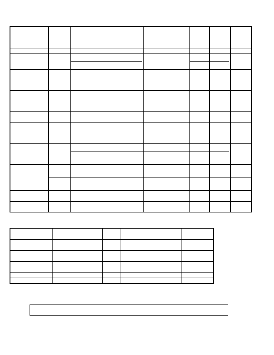
TABLE 1. ELECTRICAL TESTS
TEST
Symbol
CONDITIONS
-55
∞
C <=T
A
<= +125
∞
C
V
DD
=+15V
Unless otherwise specified
Group A
Subgroup
Device
type
Limits
Min
Limits
Max
Units
SWITCH
Logic 1 Input
Voltage
V
IH
V
DD
=4.5V
V
DD
=15V
1,2,3
All
2.0
2.0
V
Logic 0 Input
Voltage
V
IL
V
DD
=4.5V
V
DD
=15V
1
2,3
1,2,3
All
0.8
0.5
0.8
V
Input Current
I
IN
V
DD
=15V, V
IN
=0V and 15V
1,2,3
All
-0.1
0.1
µ
A
Output Voltage
High
V
OH
V
DD
=4.5V and 15V
1
2,3
All
V
CC
-.05
V
CC
-0.1
V
Output Voltage
Low
V
OL
V
DD
=4.5V and 15V
1
2,3
All
.05
0.1
V
Output Resistance
R
OUT
V
IN
=V
IL
, I
OUT
=+10mA, V
CC
=15V
1
2,3
All
10
12
Output Resistance
R
OUT
V
IN
=V
IH
, I
OUT
=-10mA, V
CC
=15V
1
2,3
All
12
13
Power-Supply
Current
I
CC
V
IN
=0V, both inputs
V
IN
=3V, both inputs
1,2,3
1
2,3
All
All
0.4
7
8
mA
Delay Time
t
D1
t
D2
Figure 1
Figure 1
9
10,11
9
10,11
All
All
30
40
50
60
ns
ns
Rise Time
t
R
Figure 1
9
10,11
All
30
40
ns
Fall Time
t
F
Figure 1
9
10,11
All
30
40
ns
FIGURE 1: Timing Diagram/Test Circuit. See Commercial Datasheet.
ORDERING
INFORMATION:
Terminal
ICL7667
ICL7667
Maxim #
Pkg.
Number
J8
TO99
5962-8766001PA
ICL7667MJA/883B
J8
1
NC
OUTA
5962-8766001GC
ICL7667MTV/883B
TO99
2
INA
NC
3
V-
INA
4
INB
V-
5
OUTB
INB
6
V
DD
NC
7
OUTA
OUTB
8
NC
V
DD
----------------------------
Electrical Characteristics of ICL7667Mxx/883B
19-0457
Rev. B
for SMD 5962-87660
Page 3 of
5
QUALITY ASSURANCE
Sampling and inspection procedures shall be in accordance with MIL-Prf-38535, Appendix A as specified in Mil-
Std-883.
Screening shall be in accordance with Method 5004 of Mil-Std-883. Burn-in test Method 1015:
1. Test Condition, A, B, C, or D.
2. TA = +125
∞
C minimum.
3. Interim and final electrical test requirements shall be specified in Table 2.
Quality conformance inspection shall be in accordance with Method 5005 of Mil-Std-883, including Groups A, B,
C, and D inspection.
Group A inspection:
1. Tests as specified in Table 2.
2. Selected subgroups in Table 1, Method 5005 of Mil-Std-883 shall be omitted.
Group C and D inspections:
a. End-point electrical parameters shall be specified in Table 1.
b. Steady-state life test, Method 1005 of Mil-Std-883:
1. Test condition A, B, C, D.
2. TA = +125
∞
C, minimum.
3. Test duration, 1000 hours, except as permitted by Method 1005 of Mil-Std-883.
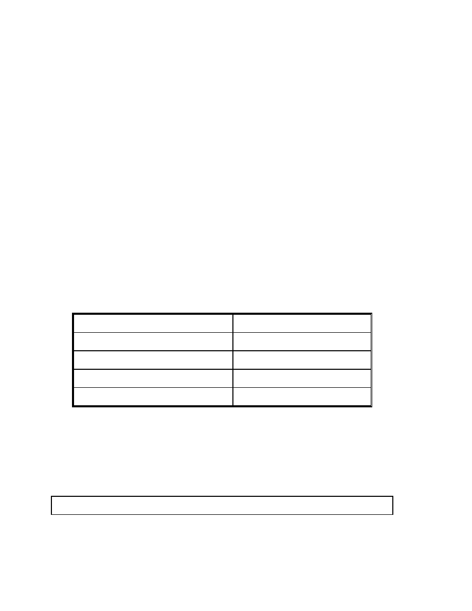
TABLE 2. ELECTRICAL TEST REQUIREMENTS
Mil-Std-883 Test Requirements
Subgroups
per Method 5005, Table 1
Interim Electric Parameters
Method 5004
1
Final Electrical Parameters
Method 5005
1*, 2, 3, 9
Group A Test Requirements
Method 5005
1, 2, 3, 9, 10, 11
Group C and D End-Point Electrical Parameters
Method 5005
1
* PDA applies to Subgroup 1 only.
----------------------------
Electrical Characteristics of ICL7667Mxx/883B
19-0457
Rev. B
for SMD 5962-87660
Page 4 of
5