 | –≠–ª–µ–∫—Ç—Ä–æ–Ω–Ω—ã–π –∫–æ–º–ø–æ–Ω–µ–Ω—Ç: MAX1002C | –°–∫–∞—á–∞—Ç—å:  PDF PDF  ZIP ZIP |
_______________General Description
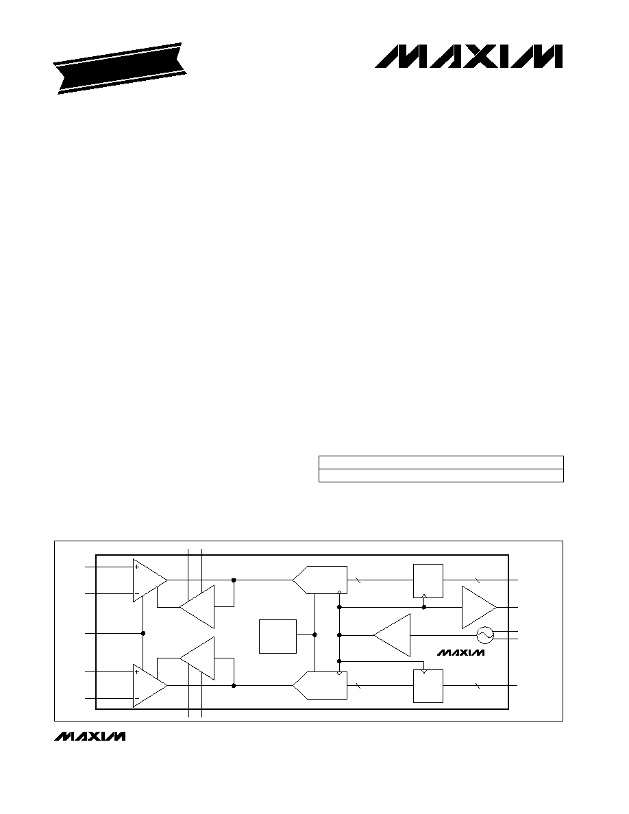
The MAX1002 is a dual, 6-bit analog-to-digital converter
(ADC) that combines high-speed, low-power operation
with a user-selectable input range, an internal refer-
ence, and a clock oscillator. The dual, parallel ADCs
are designed to convert in-phase (I) and quadrature
(Q) analog signals into two 6-bit offset-binary-coded
digital outputs at sampling rates up to 60Msps while
achieving typical integral nonlinearity (INL) and differ-
ential nonlinearity (DNL) of ±1/4LSB. The ability to
interface directly with baseband I and Q signals makes
the MAX1002 ideal for use in direct-broadcast satellite,
VSAT, and QAM16 demodulation applications.
The MAX1002 input amplifiers feature true differential
inputs, a 55MHz -0.5dB analog bandwidth, and user-
programmable input full-scale ranges of 125mVp-p,
250mVp-p, or 500mVp-p. With an AC-coupled input
signal, matching performance between input channels
is typically 0.1dB gain, 1/4LSB offset, and 0.5∞ phase.
Dynamic performance is 5.85 effective number of bits
(ENOB) with a 20MHz analog input signal, or 5.78
ENOB with a 50MHz input signal.
The MAX1002 operates with a single +5V power supply
and provides TTL-compatible digital outputs. The device
is available in the commercial temperature range (0∞C to
+70∞C) and comes in a 36-pin SSOP package.
________________________Applications
Direct Broadcast Satellite (DBS) Receivers
VSAT Receivers
Wide Local Area Networks (WLAN)
Cable Television Set-Top Boxes
____________________________Features
o
±1/4LSB INL and DNL, Typical
o
1/4LSB (typ) Channel-to-Channel Offset Matching
o
0.1dB Gain and 0.5∞ Phase Matching, Typical
o
Internal Bandgap Voltage Reference
o
Two Matched 6-Bit, 60Msps ADCs
o
Excellent Dynamic Performance:
5.85 ENOB with 20MHz Analog Input
5.7 ENOB with 50MHz Analog Input
o
Internal Oscillator with Overdrive Capability
o
55MHz (-0.5dB) Bandwidth Input Amplifiers
with True Differential Inputs
o
User-Selectable Input Full-Scale Range
(125mVp-p, 250mVp-p, or 500mVp-p)
o
Single-Ended or Differential Input Drive
o
+5V Single Supply
o
TTL Outputs
o
90Msps Upgrade with +3.3V CMOS-Compatible
Output Available (MAX1003)
MAX1002
Low-Power, 60Msps, Dual, 6-Bit ADC
________________________________________________________________
Maxim Integrated Products
1
MAX1002
DATA
BUFFER
Q
CLOCK
DRIVER
D0I≠D5I
DCLK
TNK+
TNK-
DQ0≠DQ5
INPUT
AMP
I
IIN+
IIN-
GAIN
QIN+
QIN-
CLOCK
OUT
DATA
BUFFER
I
6
ADC
I
ADC
Q
VREF
VREF
BANDGAP
REFERENCE
OFFSET
CORREC-
TION Q
OFFSET
CORREC-
TION I
INPUT
AMP
Q
QOCC+
QOCC-
IOCC+
IOCC-
6
6
6
_________________________________________________________Functional Diagram
19-1270; Rev 0; 7/97
PART
MAX1002CAX
0∞C to +70∞C
TEMP. RANGE
PIN-PACKAGE
36 SSOP
EVALUATION KIT
AVAILABLE
______________Ordering Information
Pin Configuration appears at end of data sheet.
For free samples & the latest literature: http://www.maxim-ic.com, or phone 1-800-998-8800
For small orders, phone 408-737-7600 ext. 3468.
MAX1002
Low-Power, 60Msps, Dual, 6-Bit ADC
2
_______________________________________________________________________________________
ABSOLUTE MAXIMUM RATINGS
DC ELECTRICAL CHARACTERISTICS
(V
CC
, V
CCO
= +5V ±5%; T
A
= T
MIN
to T
MAX
; unless otherwise noted.)
Stresses beyond those listed under "Absolute Maximum Ratings" may cause permanent damage to the device. These are stress ratings only, and functional
operation of the device at these or any other conditions beyond those indicated in the operational sections of the specifications is not implied. Exposure to
absolute maximum rating conditions for extended periods may affect device reliability.
V
CC
to GND .........................................................-0.3V to +6.5V
V
CCO
to OGND.........................................................-0.3V, +6.5V
GND to OGND .........................................................-0.3V, +0.3V
Digital and Clock Output Pins to OGND ........-0.3V, V
CCO
(<10sec)
All Other Pins to GND..................................................-0.3V, V
CC
Continuous Power Dissipation (T
A
= +70∞C)
SSOP (derate 45mW/∞C above +70∞C) ......................941mW
Operating Temperature Range...............................0∞C to +70∞C
Storage Temperature Range .............................-65∞C to +150∞C
Lead Temperature (soldering, <10sec)...........................+300∞C
CONDITIONS
LSB
-0.5
±0.25
0.5
INL
Integral Nonlinearity
Bits
6
RES
Resolution
UNITS
MIN
TYP
MAX
SYMBOL
PARAMETER
GAIN = open (mid gain)
GAIN = V
CC
(high gain)
No missing codes over temperature
237.5
250
262.5
V
FSM
118.75
125
131.25
V
FSH
LSB
-0.5
±0.25
0.5
DNL
Differential Nonlinearity
Other analog input driven with external source
(Note 2)
Guaranteed by design
V
1.75
2.75
V
CM
GAIN = GND (low gain)
Common-Mode Voltage Range
pF
3
5
C
IN
Input Capacitance
k
13
20
29
R
IN
Input Resistance
V
2.25
2.35
2.45
V
AOC
Input Open-Circuit Voltage
mVp-p
475
500
525
V
FSL
Full-Scale Input Range
Other oscillator input tied to V
CC
+ 0.3V
I
SOURCE
= 50µA
V
2.4
V
OH
Digital Outputs Logic-High
Voltage
k
4.8
8
12.1
R
OSC
Oscillator Input Resistance
I
SINK
= 400µA
V
0.5
V
OL
Digital Outputs Logic-Low
Voltage
V
CC
= 4.75V to 5.25V (Note 3)
20MHz, FS I & Q analog inputs,
C
LOAD
= 15pF (Note 4)
mW
380
PD
Power Dissipation
mA
24
I
CCO
Digital Outputs Supply Current
dB
-75
-40
PSRR
Power-Supply Rejection Ratio
mA
63
104
I
CC
Supply Current
DC ACCURACY
(Note 1)
INVERTING AND NONINVERTING ANALOG INPUTS
OSCILLATOR INPUTS
DIGITAL OUTPUTS (DI0≠DI5, DQ0≠DQ5)
POWER SUPPLY
MAX1002
Low-Power, 60Msps, Dual, 6-Bit ADC
_______________________________________________________________________________________
3
AC ELECTRICAL CHARACTERISTICS
(V
CC,
V
CCO
= +5V ±5%; T
A
= +25∞C; unless otherwise noted.)
Note 1:
Best straight-line linearity method.
Note 2:
A typical application will AC couple the analog input to the DC bias level present at the analog inputs (typically 2.35V).
However, it is also possible to DC couple the analog input (using differential or single-ended drive) within this common-
mode input range (Figures 4, 5).
Note 3:
PSSR is defined as the change in the mid-gain, full-scale range as a function of the variation in V
CC
supply voltage
(expressed in decibels).
Note 4:
The current in the V
CCO
supply is a strong function of the capacitive loading on the digital outputs. To minimize supply
transients and achieve the best dynamic performance, reduce the capacitive loading effects by keeping line lengths on the
digital outputs to a minimum.
Note 5:
Offset-correction compensation enabled, 0.22µF at Q and I compensation inputs (Figures 2, 3).
Note 6:
t
PD
and t
SKEW
are measured from the 1.4V level of the output clock, to the 1.4V level of either the rising or falling edge of a
data bit. t
DCLK
is measured from the 50% level of the clock overdrive signal on TNK+ to the 1.4V level of D
CLK
. The capac-
itive load on the outputs is 15pF.
Gain = GND, open, V
CC
GAIN = open (mid gain),
V
IN
= 50MHz, -1dB below FS
GAIN = open (mid gain)
5.7
ENOB
M
5.6
5.85
Effective Number of Bits
Gain = open (mid gain)
Gain = V
CC
(low gain)
Q channel
I channel
dB
CONDITIONS
MHz
55
BW
Analog Input -0.5dB Bandwidth
Msps
60
f
MAX
Maximum Sample Rate
-55
XTLK
Gain = V
CC
(high gain)
Crosstalk Between ADCs
LSB
-0.5
0.5
OFF
Input Offset (Note 5)
-0.5
0.5
dB
35.4
37
SINAD
Signal-to-Noise and Distortion
Ratio
Bits
5.85
ENOB
L
5.8
ENOB
H
(Note 5)
dB
-0.2
±0.1
0.2
AM
Amplitude Match Between
ADCs
LSB
-0.5
±0.25
0.5
OMM2
Offset Mismatch Between ADCs
(Note 6)
(Note 6)
ns
3.6
t
SKEW
Data Valid Skew
ns
7.1
t
PD
DCLK to Data-Propagation
Delay
degrees
-2
±0.5
2
PM
UNITS
MIN
TYP
MAX
SYMBOL
PARAMETER
Phase Match Between ADCs
TNK+ to DCLK (Note 6)
ns
5.3
t
DCLK
Input to DCLK Delay
ns
5.5
t
AP
Aperture Delay
clock
cycle
1
PD
Pipeline Delay
DYNAMIC PERFORMANCE
(GAIN = open; external 60MHz clock (Figure 7); V
INI
, V
INIQ
= 20MHz sine; amplitude -1dB below FS;
unless otherwise noted.)
TIMING CHARACTERISTICS
(data outputs: R
L
= 1M
, C
L
= 15pF, Figure 8)
MAX1002
Low-Power, 60Msps, Dual, 6-Bit ADC
4
_______________________________________________________________________________________
__________________________________________Typical Operating Characteristics
(V
CC,
V
CCO
= +5V ±5%; MAX1002/MAX1003 evaluation kit; T
A
= +25∞C; unless otherwise noted.)
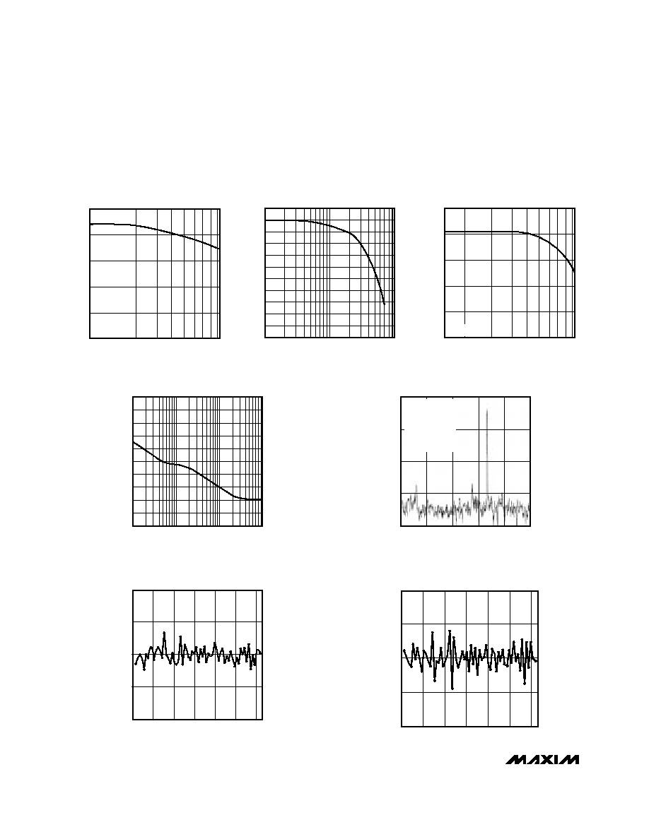
6.0
5.0
10
100
EFFECTIVE NUMBER OF BITS
vs. ANALOG INPUT FREQUENCY
5.2
MAX1002-01
ANALOG INPUT FREQUENCY (MHz)
ENOB (bits)
5.4
5.6
5.8
f
CLK
= 60Msps
-1.0
1
10
100
ANALOG INPUT BANDWIDTH
-0.8
MAX1002-02
ANALOG INPUT FREQUENCY (MHz)
MAGNITUDE (dB) -0.6
-0.2
-0.4
0
5.5
10
100
EFFECTIVE NUMBER OF BITS
vs. SAMPLING FREQUENCY
5.6
MAX1002-03
SAMPLING FREQUENCY (MHz)
ENOB
5.7
5.9
5.8
6.0
f
IN
= 20MHz
-50
-70
-150
1k
100k
1M
OPEN-LOOP PHASE NOISE
vs. FREQUENCY
-130
-90
-110
MAX1002-TOC4
FREQUENCY (Hz)
PHASE NOISE (dBc)
10k
0.50
-0.50
DIFFERENTIAL NONLINEARITY
vs. CODE
-0.25
0.25
MAX1002-06
CODE
DNL (LSB)
0
0
64
10
20
30
40
50
60
0.50
-0.50
DIFFERENTIAL NONLINEARITY
vs. CODE
-0.25
0.25
MAX1002-07
DNL (LSB)
0
0
64
10
20
30
40
50
60
-80
-40
-60
-20
0
0
6
12
18
24
30
FFT PLOT
MAX1002-05
FREQUENCY (MHz)
f
IN
= 19.930MHz
f
CLK
= 60.000MHz
1024 POINTS
AC COUPLED
SINGLE ENDED
AVERAGED
_______________Detailed Description
Converter Operation
The MAX1002 contains two 6-bit analog-to-digital con-
verters (ADCs), a buffered voltage reference, and oscil-
lator circuitry. The ADCs use a flash-conversion
technique to convert an analog input signal into a 6-bit
parallel digital output code. The MAX1002's unique
design includes 63 fully differential comparators and a
proprietary encoding scheme that ensures no more
than 1LSB dynamic encoding error. The control logic
interfaces easily to most digital signal processors
(DSPs) and microprocessors (µPs) with +5V CMOS-
compatible logic interfaces. Figure 1 shows the
MAX1002 in a typical application.
Programmable Input Amplifiers
The MAX1002 has in-phase (I) and quadrature (Q) pro-
grammable-gain input amplifiers with a 55MHz
-0.5dB bandwidth and true differential inputs. To maxi-
mize performance in high-speed systems, each amplifier
has less than 5pF of input capacitance. The input ampli-
fier gain is programmed via the GAIN pin to provide
three possible input full-scale ranges (FSR) (Table 1).
MAX1002
Low-Power, 60Msps, Dual, 6-Bit ADC
_______________________________________________________________________________________
5
______________________________________________________________Pin Description
PIN
Gain-Select Input. Sets input full-scale range: 125/250/500mVp-p (Table 1).
GAIN
1
FUNCTION
NAME
Positive I-Channel Offset-Correction Compensation. Connect 0.22µF capacitor
for AC-coupled inputs (Figures 2, 3). Ground for DC-coupled inputs (Figures 4, 5).
IOCC+
2
I-Channel Noninverting Analog Input
IIN+
4
Negative I-Channel Offset-Correction Compensation. Connect 0.22µF capacitor
for AC-coupled inputs (Figures 2, 3). Ground for DC-coupled inputs (Figures 4, 5).
IOCC-
3
+5V ±5% Supply. Bypass with 0.01µF capacitor to GND (Pin 7).
V
CC
6
+5V ±5% Supply. Bypass with 0.01µF capacitor to GND (Pin 11).
V
CC
8
Analog Ground
GND
7, 11, 12,
18, 19
I-Channel Inverting Analog Input
IIN-
5
Negative Oscillator/Clock Input
TNK-
10
Q-Channel Inverting Analog Input
QIN-
14
+5V ±5% Supply. Bypass with 0.01µF capacitor to GND (Pin 12).
V
CC
13
Negative Q-Channel Offset-Correction Compensation. Connect 0.22µF capacitor
for AC-coupled inputs (Figures 2, 3). Ground for DC-coupled inputs (Figures 4, 5).
QOCC-
16
Q-Channel Digital Outputs 0≠5. DQ5 is the most significant bit (MSB).
DQ5≠DQ0
20≠25
Positive Q-Channel Offset-Correction Compensation. Connect 0.22µF capacitor
for AC-coupled inputs (Figures 2, 3). Ground for DC-coupled inputs (Figures 4, 5).
QOCC+
17
Q-Channel Noninverting Analog Input
QIN+
15
Positive Oscillator/Clock Input
TNK+
9
Digital Output Ground
OGND
27
I-Channel Digital Outputs 0≠5. DI5 is the most significant bit (MSB).
DI0≠DI5
30≠35
Digital Clock Output. Frames the output data.
DCLK
29
+5V ±5% Digital Supply. Bypass each with 47pF to OGND (Pin 27).
V
CCO
26, 28
+5V ±5% Supply. Bypass with 0.01µF to GND (Pin 19).
V
CC
36
250
Open
125
V
CC
GAIN
500
GND
INPUT FULL-SCALE RANGE
(mVp-p)
Table 1. Input Amplifier Programming