
For free samples & the latest literature: http://www.maxim-ic.com, or phone 1-800-998-8800.
For small orders, phone 408-737-7600 ext. 3468.
_______________General Description
The MAX1005 is a combined digitizer and reconstruc-
tion integrated circuit designed to work in systems that
demodulate and modulate communications signals. It
integrates IF undersampling and signal synthesis func-
tions into a single, low-power circuit. Its analog-to-
digital converter (ADC) is used to directly sample or
undersample a downconverted RF signal, while its
digital-to-analog converter (DAC) recreates the IF sub-
carrier and transmission data. The MAX1005's ADC is
ideal for undersampling applications, due to the analog
input amplifier's wide (15MHz) bandwidth. The DAC
has very low glitch energy, which minimizes the trans-
mission of unwanted spurious signals. An on-chip
reference provides for low-noise ADC and DAC conver-
sions.
The MAX1005 provides a high level of signal integrity
from a low power budget. It operates from a single
power supply, or from separate analog and digital sup-
plies with independent voltages ranging from +2.7V to
+5.5V. The MAX1005 can operate with an unregulated
analog supply of 5.5V and a regulated digital supply
down to 2.7V. This flexible power-supply operation
saves additional power in complex digital systems.
The MAX1005 has three operating modes: transmit
(DAC active), receive (ADC active), and shutdown
(ADC and DAC inactive). In shutdown mode, the total
supply current drops below 1µA. The device requires
only 2.4µs to wake up from shutdown mode. The
MAX1005 is ideal for hand-held, as well as base-station
applications. It is available in a tiny 16-pin QSOP pack-
age specified for operation over both the commercial
and extended temperature ranges.
________________________Applications
PWT1900
PHS/P
Wireless Loops
PCS/N
____________________________Features
o
Differential-Input, 5-Bit ADC
o
Differential-Output, 7-Bit DAC
o
15Msps Min Conversion Rate
o
25MHz -1dB Full-Power Bandwidth
o
44dB SFDR for ADC
39dB at 10.7MHz SFDR (Imaged) for DAC
o
Internal Voltage Reference
o
Parallel Logic Interface
o
Single-Supply Operation (+2.7V to +5.5V)
o
0.1µA Low-Power Shutdown Mode
MAX1005
IF Undersampler
________________________________________________________________
Maxim Integrated Products
1
16
15
14
13
12
11
10
9
1
2
3
4
5
6
7
8
VCCD
CLK
D0
D1
D2
D3
D4
D5
D6
TOP VIEW
MAX1005
QSOP
DGND
RXEN
TXEN
AIO+
AIO-
AGND
VCCA
__________________Pin Configuration
19-1291; Rev 0; 9/97
PART
MAX1005CEE
MAX1005EEE
-40∞C to +85∞C
0∞C to +70∞C
TEMP. RANGE
PIN-PACKAGE
16 QSOP
16 QSOP
______________Ordering Information
Functional Diagram appears at end of data sheet.

MAX1005
IF Undersampler
2
_______________________________________________________________________________________
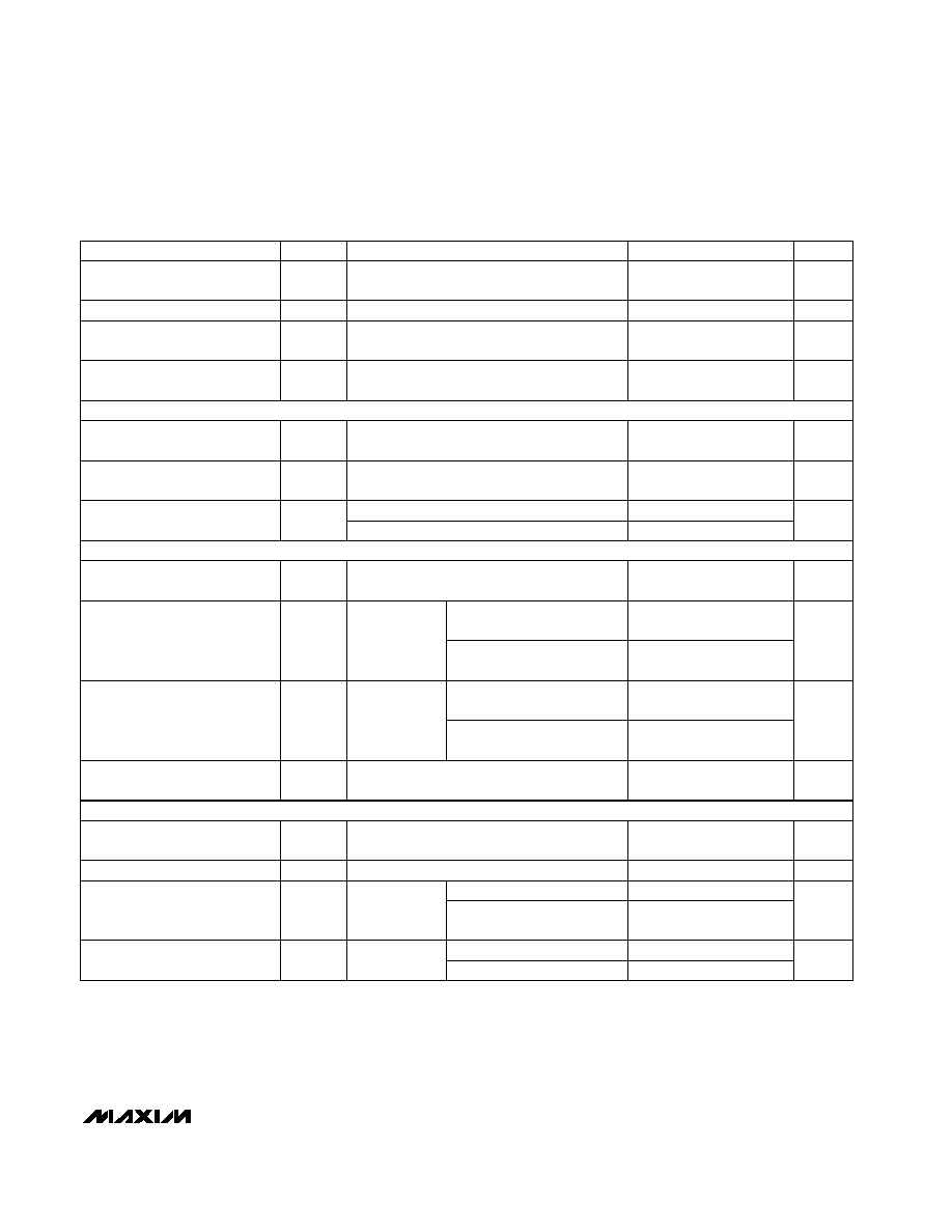
ABSOLUTE MAXIMUM RATINGS
ELECTRICAL CHARACTERISTICS
(VCCA = VCCD = 3.0V, f
CLK
= 15MHz, R
L
=
, T
A
= T
MIN
to T
MAX
, unless otherwise noted.)
Stresses beyond those listed under "Absolute Maximum Ratings" may cause permanent damage to the device. These are stress ratings only, and functional
operation of the device at these or any other conditions beyond those indicated in the operational sections of the specifications is not implied. Exposure to
absolute maximum rating conditions for extended periods may affect device reliability.
VCCA to AGND ........................................................-0.3V, +6.0V
VCCD to DGND ........................................................-0.3V, +6.0V
VCCA to VCCD ...................................................................±6.3V
Digital I/O Pins (D0≠D6, CLK, RXEN, TXEN)
to DGND .................................-0.3V to (VCCD + 0.3V) or 6.0V
(whichever is smaller)
Analog I/O Pins (AIO+, AIO-)
to AGND................................(VCCA - 1.5V) to (VCCA + 0.3V)
AGND to DGND........................................................-0.3V, +0.3V
Power Dissipation (T
A
= +70∞C)
QSOP (derate 5.90mW/∞C above 70∞C) ......................470mW
Operating Temperature Ranges
MAX1005CEE .....................................................0∞C to +70∞C
MAX1005EEE...................................................-40∞C to +85∞C
Storage Temperature Range .............................-65∞C to +150∞C
Lead Temperature (soldering, <10sec)...........................+300∞C
(Notes 9, 10)
AIO+ = AIO-
(Note 4)
(Notes 6, 7)
(Note 3)
(Note 5)
CONDITIONS
-42
dB
-42
-24
THD
Total Harmonic Distortion
mV
368
400
432
V
IN
Full-Scale Input Range
LSB
±2
Offset Error
LSB
±0.2
DNL
Differential Nonlinearity
LSB
±0.2
INL
Integral Nonlinearity
Bits
5
N
Resolution
dB
67
PSR
Power-Supply Rejection
CLK
period
0.5
DAC Latency
dBc
-50
Clock Feedthrough
µs
0.7
2.4
t
WAKE
Wakeup Time Exiting Shutdown
LSB
±0.2
±1
INL
Integral Nonlinearity
Bits
7
N
Resolution
-28
dBc
THD+N
Total Harmonic Distortion plus
Noise
39
dBc
28
39
SFDR
Spurious-Free Dynamic Range
LSB
±0.2
±1
DNL
Differential Nonlinearity
LSB
±1
Offset Error
mVp-p
736
800
864
V
OUT
Transmit Full-Scale Output Voltage
UNITS
MIN
TYP
MAX
SYMBOL
PARAMETER
VCCA = VCCD = 2.7V to 5.5V
VCCA = VCCD = 3.0V
VCCA = VCCD = 3.0V
VCC_ (A or D or both) = 3.0V ±100mVp-p at
100kHz
VCCA = VCCD = 2.7V to 5.5V
VCCA = VCCD = 3.0V
(Note 9)
(Note 9)
4.9
Bits
4.5
4.9
ENOB
Effective Number of Bits
44
dB
24
44
SFDR
Spurious-Free Dynamic Range
VCCA = VCCD = 2.7V to 5.5V
VCCA = VCCD = 3.0V
VCCA = VCCD = 2.7V to 5.5V
VCCA = VCCD = 3.0V
TRANSMIT DAC DC ACCURACY
(Note 1)
TRANSMIT DAC DYNAMIC PERFORMANCE
(T
A
= +25∞C) (Note 2)
TRANSMIT ADC DC ACCURACY
(Note 8)
RECEIVE ADC DYNAMIC PERFORMANCE
(T
A
= +25∞C) (Note 8)
MAX1005
IF Undersampler
_______________________________________________________________________________________
3
ELECTRICAL CHARACTERISTICS (continued)
(VCCA = VCCD = 3.0V, f
CLK
= 15MHz, R
L
=
, T
A
= T
MIN
to T
MAX
, unless otherwise noted.)
VCCD = 2.7V
to 5.5V
VCCD = 2.7V
to 5.5V
D0≠D4, VCCD = 2.7V to 5.5V, I
SINK
= 50µA
D0≠D4, VCCD = 2.7V to 5.5V,
I
SOURCE
= 200µA
VCCA = VCCD = 3.0V, C
L
12.5pF,
RXEN = TXEN
VCCA = VCCD
= 3.0V,
C
L
12.5pF
AIO+ or AIO- to GND
Differential between AIO+ and AIO-
VCCA = VCCD
= 3.0V,
C
L
12.5pF
CONDITIONS
-0.1
0.5
V
0.3VCCD
V
IL
Input Low Voltage
VCCD -
VCCD +
0.5
0.1
V
0.7VCCD
V
IH
Input High Voltage
V
0
0.5
V
OL
Output Low Voltage
V
VCCD - 1.0
VCCD
V
OH
Output High Voltage
µA
<0.1
5
ICCA +
ICD
Shutdown Supply Current
3.0
5.6
mA
4.0
6.4
ICCD
Digital Supply Current
2.5
3.8
mA
9.0
14.8
ICCA
Analog Supply Current
µs
0.6
2.4
t
WAKE
Wakeup Time Exiting Shutdown
Mode
Msps
15
MHz
15
25
Input Full-Power Bandwidth
(-1dB)
Conversion Rate
V
2.7
5.5
VCCA,
VCCD
Supply Voltage
pF
4
C
IN
Input Capacitance (Note 6)
LSB
<0.1
PSR
Power-Supply Rejection
k
1.56
2.00
2.44
R
IN
Input Resistance
ppm/∞C
-2000
TCR
IN
Input Resistance Temperature
Coefficient
UNITS
MIN
TYP
MAX
SYMBOL
PARAMETER
RXEN, TXEN
D0≠D6, CLK
RXEN, TXEN
D0≠D6, CLK
V
IN
= 90% of full scale
RXEN = 0, TXEN = 1,
ADC off, DAC on
RXEN = 1, TXEN = 0,
ADC on, DAC off
VCC_ (A or D or both) = 3.0V ±100mVp-p at
100kHz
T
A
= +25∞C, differential between AIO+ and
AIO-
RXEN = 0, TXEN = 1,
ADC off, DAC on
RXEN = 1, TXEN = 0,
ADC on, DAC off
4
DIGITAL INPUTS/OUTPUTS (D0≠D6, RXEN, TXEN, CLK)
(Note 12)
POWER REQUIREMENTS
ANALOG INPUT/OUTPUT (AIO+, AIO-)
(Note 11)

CONDITIONS
MAX1005
IF Undersampler
4
_______________________________________________________________________________________
ELECTRICAL CHARACTERISTICS (continued)
(VCCA = VCCD = 3.0V, f
CLK
= 15MHz, R
L
=
, T
A
= T
MIN
to T
MAX
, unless otherwise noted.)
RXEN, TXEN;
VCCD = 2.7V
to 3.6V
D0≠D6, CLK; VCCD = 2.7V to 5.5V
C
L
12.5pF
T
A
= +25∞C (Note 6)
T
A
= +25∞C (Note 6)
RXEN, TXEN;
VCCD = 3.6V
to 5.5V
D0≠D6, CLK; TXEN = 1, RXEN = 0 (Note 6)
CONDITIONS
±2
±1
µA
-1
7
I
IN
Input Current
ns
13
20
t
DO
ADC CLK to Output Data Valid
%
45
55
CLK Duty Cycle
ns
5
0.3
t
HOLD
DAC Data Hold Time
ns
5
0.6
t
DS
DAC Data Setup Time
±1
±4
pF
8
C
IN
Input Capacitance
UNITS
MIN
TYP
MAX
SYMBOL
PARAMETER
TXEN = 0 and RXEN = 1, or
TXEN = 1 and RXEN = 0
TXEN = RXEN
TXEN = RXEN
TXEN = 0 and RXEN = 1, or
TXEN = 1 and RXEN = 0
Note 1:
TXEN = 1, RXEN = 0. All DAC transfer function parameters are measured differentially from AIO+ to AIO- using the End-
Point Linearity method.
Note 2:
f
IN
= 4.3MHz digital sine wave applied to DAC data inputs; f
CLK
= 15MHz. The reference frequency (f
REF
) is defined to be
10.7MHz (f
CLK
- f
IN
). All frequency components present in the DAC output waveform except for f
REF
and f
IN
are consid-
ered spurious.
Note 3:
For DAC SFDR measurements, the amplitude of f
REF
(10.7MHz) is compared to the amplitudes of all frequency compo-
nents of the output waveform except for f
IN
(4.3MHz).
Note 4:
For DAC measurements, THD+N is defined as the ratio of the square-root of the sum-of-the-squares of the RMS values of
all harmonic and noise components of the output waveform (except for f
IN
and f
REF
) to the RMS amplitude of the f
REF
com-
ponent.
Note 5:
Clock feedthrough is defined as the difference in amplitude between the f
REF
component and the f
CLK
component when
measured differentially from AIO+ to AIO-.
Note 6:
Guaranteed by design. Not production tested.
Note 7:
The DAC input interface is a master/slave register. An additional half clock cycle is required for data at the digital inputs to
propagate through to the DAC switches.
Note 8:
RXEN = 1, TXEN = 0. Unless otherwise noted, for all receive ADC measurements, the analog input signal is applied differ-
entially from AIO+ to AIO-, specified using the Best-Fit Straight-Line Linearity method.
Note 9:
f
IN
= 10.7MHz, f
CLK
= 15MHz. Amplitude is 1dB below full-scale. The reference frequency (f
REF
) is defined to be 4.3MHz
(f
CLK
- f
IN
). All components except for f
REF
and f
IN
are considered spurious.
Note 10:
Receive ADC THD measurements include the first five harmonics.
Note 11:
CAUTION: Operation of the analog inputs AIO+ and AIO- (pins 4 and 5) at more than 1.5V below VCCA could cause
latchup and possible destruction of the part. Avoid shunt capacitances to GND on these pins. If shunt capacitances are
required, then bypass these pins only to VCCA.
Note 12:
All digital input signals are measured from 50% amplitude reference points. All digital output signal propagation delays are
measured to V
OH(AC)
for rising output signals and to V
OL(AC)
for falling output signals. The values for V
OH(AC)
and V
OL(AC)
as a function of the VCCD supply are shown in the following table:
VCCD (V)
V
OH(AC)
(V)
V
OL(AC)
(V)
2.7 to 3.3
VCCD - 1.1
0.5
3.3 to 5.5
2/3 x VCCD
0.5
TIMING CHARACTERISTICS
(Data Outputs: R
L
= 1M
, C
L
= 15pF, T
A
= T
MIN
to T
MAX
, unless otherwise noted.) (Note 12)

MAX1005
IF Undersampler
_______________________________________________________________________________________
5
-0.50
-0.30
-0.40
-0.10
-0.20
0.10
0.00
0.20
0.40
0.30
0.50
-15
-9
-6
-3
-12
0
3
6
12
9
15
RECEIVE ADC
INTEGRAL NONLINEARITY
MAX1005-01
CODE
INL (LSB)
-0.50
-0.30
-0.40
-0.10
-0.20
0.10
0.00
0.20
0.40
0.30
0.50
-15
-9
-6
-3
-12
0
3
6
12
9
15
RECEIVE ADC
DIFFERENTIAL NONLINEARITY
MAX1005-02
CODE
DNL (LSB)
-0.5
-0.3
-0.4
-0.1
-0.2
0.1
0
0.2
0.4
0.3
0.5
-64
-32
-16
-48
0
16
32
48
64
TRANSMIT DAC
INTEGRAL NONLINEARITY
MAX1005-03
CODE
INL (LSB)
-0.5
-0.3
-0.4
-0.1
-0.2
0.1
0
0.2
0.4
0.3
0.5
-64
-32
-16
-48
0
16
32
48
64
TRANSMIT DAC
DIFFERENTIAL NONLINEARITY
MAX1005-04
CODE
DNL (LSB)
-70
-40
-50
-60
-30
-20
-10
0
10
20
30
0
2.930
1.465
4.395
5.860
7.325
RECEIVE ADC FFT PLOT
MAX1005-05
FREQUENCY (MHz)
AMPLITUDE (dB)
f
IN
= 10.7MHz
f
CLK
= 15MHz
256 POINTS
-7
-6
-5
1
10
100
FULL POWER ANALOG
INPUT BANDWIDTH
MAX1005-06
ANALOG INPUT FREQUENCY (MHz)
AMPLITUDE (dB)
-4
-3
-2
-1
0
V
IN
= 90% OF FULL SCALE
__________________________________________Typical Operating Characteristics
(VCCA = VCCD = 3.0V, T
A
= +25∞C, unless otherwise noted.)