 | –≠–ª–µ–∫—Ç—Ä–æ–Ω–Ω—ã–π –∫–æ–º–ø–æ–Ω–µ–Ω—Ç: MAX1007 | –°–∫–∞—á–∞—Ç—å:  PDF PDF  ZIP ZIP |
________________General Description
The MAX1007 is a multifunctional integrated circuit
designed for high-performance mobile radios. It
includes one 8-bit analog-to-digital converter (ADC),
and two 7-bit and two 6-bit digital-to-analog converters
(DACs) for functions including radio-frequency (RF)
power sensing and antenna-diversity selection.
The ADC provides for power sense, receive-signal
strength intensity (RSSI) measurements and system
supervision. In the power-sense mode, the ADC con-
verts the power-sensing circuitry signal (representing
either the transmitted (Tx) or received (Rx) RF power)
into a digital code, ensuring optimum Tx power setting
and Rx signal analysis. An additional direct input to the
ADC provides for system-supervision measurements,
such as power-supply voltages, battery voltage, and
temperature.
Four DAC blocks typically control DC levels in radios.
As part of the Maxim PWT1900 chip set, the two 7-bit
DACs control the gain settings and the two 6-bit DACs
control the varactor diodes to tune a TCXO and bias a
GaAs amplifier. Each DAC register and output can be
updated independently, providing maximum flexibility.
For antenna diversity, a magnitude-comparison circuit
captures and compares two peak signals. A latched
logic-comparator output reveals which signal has the
largest magnitude. The MAX1007 also includes an on-
board voltage reference for the ADC and DACs.
The MAX1007 offers a high level of signal integrity with
minimal power dissipation. Single-supply operation
ranges from +2.85V to +3.6V. To further save power, there
are two shutdown modes: standby and total shutdown.
Standby is a partial shutdown that keeps the bandgap
reference and the 2.4V reference generator active. Total
shutdown disables all circuit blocks except the serial
interface, reducing supply current to less than 1µA.
The MAX1007 is available in a 24-pin SSOP and is
specified for commercial and extended temperature
ranges.
________________________Applications
PWT1900
Wireless Communications:
Cellular Radios
PMR/SMR
PCS Radios
WLL
____________________________Features
o
Multi-Input 8-Bit ADC
o
Two 7-Bit DACs with Buffered Outputs
o
Two 6-Bit DACs: Buffered/Unbuffered
o
Power-Sense Conditioning Circuitry
o
RSSI Measurement
o
Antenna-Diversity Circuitry
o
Internal Reference
o
Serial-Logic Interface
o
+2.85V to +3.6V Single-Supply Operation
o
Two Shutdown Modes
MAX1007
Mobile-Radio Analog Controller
________________________________________________________________
Maxim Integrated Products
1
19-1180; Rev 0; 6/98
PART
MAX1007CAG
MAX1007EAG
-40∞C to +85∞C
0∞C to +70∞C
TEMP. RANGE
PIN-PACKAGE
24 SSOP
24 SSOP
Ordering Information
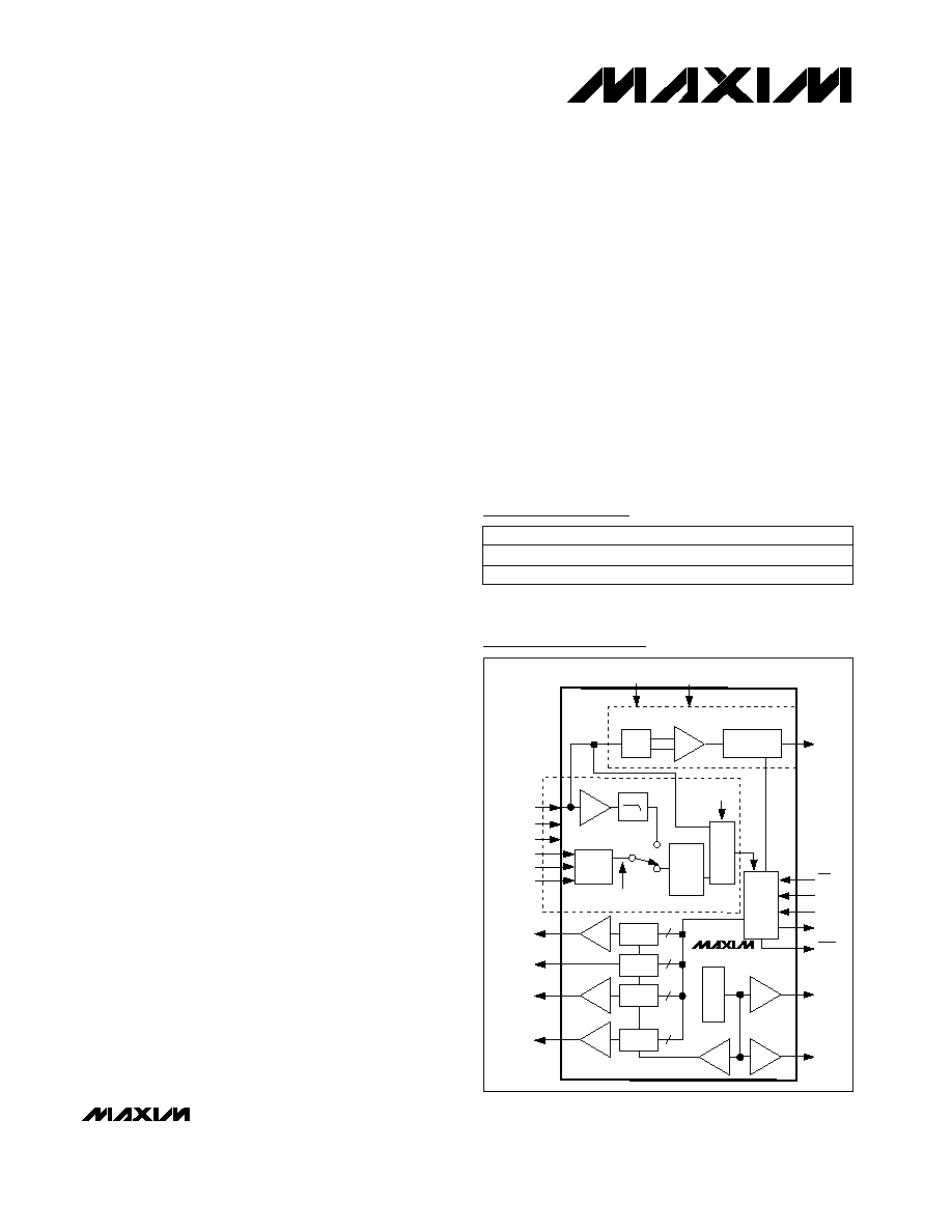
Pin Configuration appears at end of data sheet.
CS
SCLK
DIN
7
DOUT
SDAC
CH0
ADC
PEAK
DETECTOR
POWER
SENSE
RPS
RSSI
FPS1
FPS2
SDAC
XDAC
SDG
GDAC
KDAC
CH1
REFERENCE
PSBIAS
SERIAL
INTERFACE
PSDCTRL
PREAMBLE-SWITCHED DIVERSITY
POWER SENSE CIRCUITRY
PSDWDW
DUAL
T/H
VREF
XDAC
GDAC
KDAC
REF
PSOUT
BANT
ADC CTRL
PKWDW
6
6
7
D FLIP-FLOP
MAX1007
Functional Diagram
For free samples & the latest literature: http://www.maxim-ic.com, or phone 1-800-998-8800.
For small orders, phone 408-737-7600 ext. 3468.
MAX1007
Mobile-Radio Analog Controller
2
_______________________________________________________________________________________
ABSOLUTE MAXIMUM RATINGS
ELECTRICAL CHARACTERISTICS
(AV
DD
= DV
DD
= +2.85V to +3.6V, f
SCLK
= 1.152MHz, T
A
= T
MIN
to T
MAX
, unless otherwise noted.)
Stresses beyond those listed under "Absolute Maximum Ratings" may cause permanent damage to the device. These are stress ratings only, and functional
operation of the device at these or any other conditions beyond those indicated in the operational sections of the specifications is not implied. Exposure to
absolute maximum rating conditions for extended periods may affect device reliability.
AV
DD
or DV
DD
to AGND or DGND ...........................-0.3V to +6V
Digital Inputs to DGND.............................................-0.3V to +6V
Analog Inputs to AGND............................................-0.3V to +6V
REF to AGND............................................................-0.3V to +6V
AGND to DGND .................................................................± 0.3V
AV
DD
to DV
DD
....................................................................± 0.3V
Maximum Current into Any Pin............................................50mA
Continuous Power Dissipation (T
A
= +70∞C)
SSOP (derate 8.0mW/∞C above +70∞C) ......................640mW
Operating Temperature Ranges
MAX1007CAG.....................................................0∞C to +70∞C
MAX1007EAG ..................................................-40∞C to +85∞C
Storage Temperature Range .............................-65∞C to +150∞C
Lead Temperature (soldering, 10sec) .............................+300∞C
AV
DD
, DV
DD
RxEN = 1, TxEN = 1; AV
DD
= DV
DD
= 3V
RxEN = 1, TxEN = 0; AV
DD
= DV
DD
= 3V; PKWDW and
ADCCTRL as per state B on Figure 1
RxEN = 1, TxEN = 0; AV
DD
= DV
DD
= 3V;
PKWDW = ADCCTRL = DGND
RxEN = 1, TxEN = 0; AV
DD
= DV
DD
= 3V; PKWDW and
ADCCTRL as per state B on Figure 1. PSDWDW and PSD-
CNTRL as per state D on Figure 2
RxEN = 0, TxEN = 1; AV
DD
= DV
DD
= 3V;
PKWDW = ADCCTRL = DGND
RxEN = 0, TxEN = 1; AV
DD
= DV
DD
= 3V;
PKWDW and ADCCTRL as per state B on Figure 1
RxEN = 1, TxEN = 0; AV
DD
= DV
DD
= 3V; PKWDW and
ADCCTRL as per state C on Figure 1
RxEN = 0, TxEN = 1; AV
DD
= DV
DD
= 3V;
PKWDW and ADCCTRL as per state C on Figure 1
CONDITIONS
mA
1.24
3.5
Standby:
XDAC, GDAC, Ref, RefBuf Active
mA
4.07
10.5
Receive Mode 4:
KDAC, XDAC, ADC, RSSI
Buffer, Ref, RefBuf, PSD
Circuit Active
mA
11.2
31
Receive Mode 3:
KDAC, XDAC, ADC, Peak
Detector RSSI Buffer, Ref,
RefBuf Active
V
2.85
3.0
3.6
Supply Voltages
mA
2.95
Receive Mode 2:
KDAC, XDAC, Peak Detector,
RSSI Buffer, Ref, RefBuf Active
mA
1.24
3.5
Receive Mode 1:
KDAC, XDAC, Ref, RefBuf
Active
mA
1.8
5.0
Transmit Mode 1:
All DACs, Ref, RefBuf Active
mA
4.7
Transmit Mode 2:
All DACs, PGA, REF, Peak
Detector, PSBIAS, I
SOURCE
,
RefBuf Active
mA
12.2
32
Transmit Mode 3:
All DACs, PGA, REF, Peak
Detector, PSBIAS, I
SOURCE
,
RefBuf, ADC Active
UNITS
MIN
TYP
MAX
PARAMETER
RxEN = 0, TxEN = 0; AV
DD
= DV
DD
= 3V;
ADCCTRL = PSDCTRL = PKWDW = PSDWDW = DGND;
SCLK not active, either high or low
µA
1
10
Total Shutdown
POWER-SUPPLY REQUIREMENTS
SUPPLY CURRENTS
[I(AV
DD
) + I(DV
DD
)] (Note 1)

MAX1007
Mobile-Radio Analog Controller
_______________________________________________________________________________________
3
ELECTRICAL CHARACTERISTICS (continued)
(AV
DD
= DV
DD
= +2.85V to +3.6V, f
SCLK
= 1.152MHz, T
A
= T
MIN
to T
MAX
, unless otherwise noted.)
(Note 2)
2 < code
FS
2 < code
FS
2 < code
FS
C
L
= 30pF, R
L
= 40k
, settling to 5% of final value
R
L
= 40k
2 < code
FS
(Note 2)
2 < code
FS
(Note 2)
C
L
= 30pF, R
L
= 40k
No resistive load
2 < code
FS
CONDITIONS
%FSR
±10
Gain Error
LSB
±1
Offset Error
LSB
±1
Integral Nonlinearity
LSB
±1
Differential Nonlinearity
Bits
7
Resolution
µs
4
Full-Scale Step Response Time
V
2.1
2.42
2.75
Full-Scale Output Swing
V/µs
0.1
Output Slew Rate
%FSR
±10
Gain Error
LSB
±1
Offset Error
LSB
±1
Integral Nonlinearity
LSB
±1
Differential Nonlinearity
Bits
6
Resolution
LSB
±1
Differential Nonlinearity
Bits
6
Resolution
k
30
Output Resistance
LSB
±1/2
Integral Nonlinearity
LSB
±1
Offset Error
%FSR
±10
Gain Error
V
2.1
2.42
2.75
Full-Scale Output Swing
UNITS
MIN
TYP
MAX
PARAMETER
C
L
= 30pF, R
L
= 40k
, settling to 2% of final value
R
L
= 40k
C
L
= 30pF, R
L
= 40k
µs
4
Full-Scale Step Response Time
V
2.1
2.42
2.75
Full-Scale Output Swing
V/µs
0.1
Output Slew Rate
C
L
= 30pF, R
L
= 40k
, settling to within 2% of final value
µs
4
Power-Up Time from Standby
With respect to V
REF
V
REF
= 1.028V (typ)
V
REF
= 1.028V (typ)
LSB
±5
Gain Error
LSB
±2
Offset Error
µs
5.2
Conversion Time
LSB
±1
Integral Nonlinearity
LSB
±1
Differential Nonlinearity
V
0
V
REF
Input Signal Range
Bits
8
Resolution
µs
1.74
ADC Power-Up Time from Standby
V
1.028
Reference Voltage
XDAC
GDAC
SDAC, KDAC
ADC
MAX1007
Mobile-Radio Analog Controller
4
_______________________________________________________________________________________
ELECTRICAL CHARACTERISTICS (continued)
(AV
DD
= DV
DD
= +2.85V to +3.6V, f
SCLK
= 1.152MHz, T
A
= T
MIN
to T
MAX
, unless otherwise noted.)
V
IL
V
IH
SYMBOL
V
0.3V
DD
Input Voltage Low
V
0.7V
DD
Input Voltage High
V
2.42
Internal DAC Reference
µA
200
PS Bias Sink Current
V
1.87
PS Bias Voltage Output
V
0.96
1.028
1.1
Output Voltage
mV
100
300
Minimum Peak Level Detected
µs
10
20
Lowpass-Filter Time Constant
200
Pull-Down Input Resistance
µA
50
100
180
Current Source
-0.44
-6
V
V
REF
Maximum Peak Level Detected
mV
150
Offset Voltage
V/V
-0.53
Power-Sense Amp Gain (PGA)
UNITS
MIN
TYP
MAX
PARAMETER
C
IN
R
IN
I
IN
pF
10
Inpt Capacitance
k
20
Input Resistance
µA
±1
Input Current
t
8
t
7
t
6
t
5
t
4
t
3
t
2
t
1
ns
100
CS High to DOUT Disable
ns
200
434
SCLK Pulse Width Low
ns
200
434
SCLK Pulse Width High
ns
150
SCLK High to DOUT Valid
ns
100
CS Low to DOUT Valid
ns
20
CS Low to SCLK High
ns
0
DIN to SCLK Hold
ns
100
DIN Valid to SCLK Setup
t
9
ns
500
ADC Data Output Delay After
End of ADC Conversion
(Figure 4b)
V
OL
V
OH
V
0.4
Output Voltage Low
V
V
DD
- 0.4
Output Voltage High
C
L
= 20pF, R
L
= 100k
R
S
in series with C
L
, C
L
= 1nF, 200
R
S
1k
RPS, FPS1, FPS2 pulled to AGND when not
selected
Figure 3b
R
S
in series with C
L
, C
L
= 1nF, 200
R
S
1k
Reflected transmit, classes 2, 3, 4
Reflected transmit, class 1
RPS, FPS1, FPS2 to ADC input
Forward transmit
CONDITIONS
C
L
= 20pF, R
L
= 100k
Digital inputs
PSDCTRL, PSDWDW
Excluding PSDCTRL, PSDWDW
C
L
= 20pF
Digital Outputs (DOUT, BANT,
SDG
)
TIMING SPECIFICATIONS (Figure 4)
Digital Inputs (
CS
, SCLK, DIN, PKWDW, ADCCTRL, PSDWDW, PSDCTRL)
SERIAL-LOGIC INTERFACE
REFERENCE
TRANSMIT POWER SENSE
RSSI CIRCUIT
-0.5
-0.2
-0.3
-0.4
-0.1
0
0.1
0.2
0.3
0.4
0.5
0
100
50
150
200
250
300
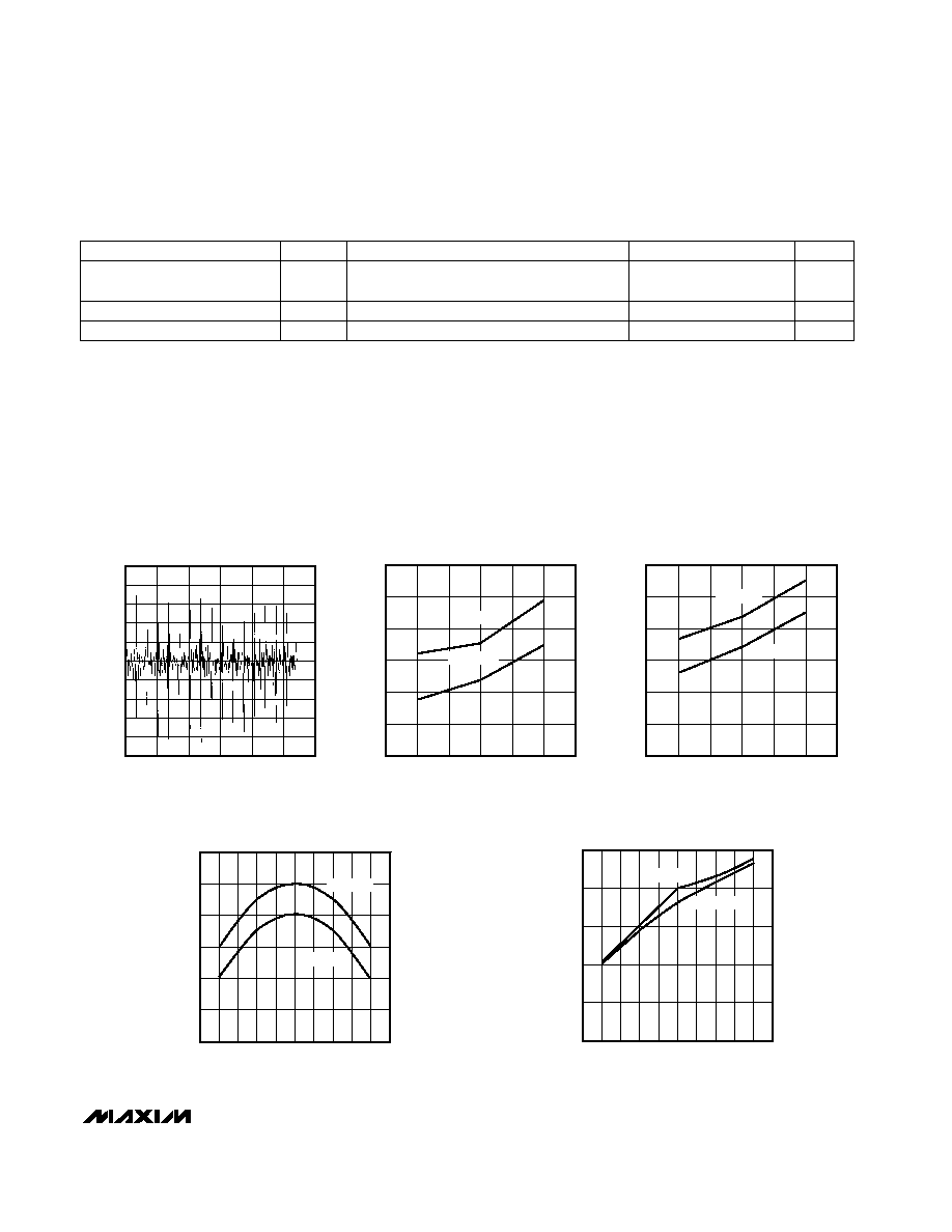
DIFFERENTIAL NONLINEARITY
MAX1007-01
CODES
DNL (LSBs)
1.25
1.35
1.30
1.45
1.40
1.50
1.55
-40
25
85
SUPPLY CURRENT vs. TEMPERATURE
(Tx MODE)
MAX1007-02
TEMPERATURE (∞C)
SUPPLY CURRENT (mA)
V
DD
= 3.6V
V
DD
= 2.85V
1.80
2.00
1.90
2.20
2.10
2.30
2.40
25
-40
85
SUPPLY CURRENT vs. TEMPERATURE
(Rx MODE)
MAX1007-03
TEMPERATURE (∞C)
SUPPLY CURRENT (mA)
V
DD
= 3.6V
V
DD
= 2.85V
1.019
1.022
1.021
1.020
1.023
1.024
1.025
-5
-40
25
55
85
REFERENCE VOLTAGE
vs. TEMPERATURE
MAX1007-04
TEMPERATURE (∞C)
REFERENCE VOLTAGE (V)
V
DD
= 3.6V
V
DD
= 2.85V
1.76
1.82
1.80
1.78
1.84
1.86
-5
-40
25
55
85
PS BIAS VOLTAGE vs. TEMPERATURE
MAX1007-05
TEMPERATURE (∞C)
PS BIAS VOLTAGE (V)
V
DD
= 3.6V
V
DD
= 2.85V
MAX1007
Mobile-Radio Analog Controller
_______________________________________________________________________________________
5
ELECTRICAL CHARACTERISTICS (continued)
(AV
DD
= DV
DD
= +2.85V to +3.6V, f
SCLK
= 1.152MHz, T
A
= T
MIN
to T
MAX
, unless otherwise noted.)
__________________________________________Typical Operating Characteristics
(T
A
= +25∞C, unless otherwise noted.)
Note 1:
All digital inputs at DV
DD
or DGND.
Note 2:
All DACs use an internal reference voltage of 2.42V.
PARAMETER
MIN
TYP
MAX
UNITS
PSDWDW Low to BANT Valid
ADCCTRL Low to RF input
200
ns
100
ns
SCLK Duty Cycle
50
%
SYMBOL
t
10
t
11
CONDITIONS
RF input on RSSI, RPS, FPS1, FPS2, or
PSBIAS, (Figure 4c)
C
L
= 20pF (Figure 4c)