For free samples & the latest literature: http://www.maxim-ic.com, or phone 1-800-998-8800
_______________General Description
The MAX101A evaluation kit (EV kit) was developed to
assist in the initial evaluation of the MAX101A high-
speed analog-to-digital converters (ADCs). The EV kit is
a two-board set comprised of a main board and a ter-
mination board.
The main board contains all the circuitry needed to
evaluate the initial performance of this flash converter,
which combines high-speed analog and digital circuitry
and requires special attention to circuit layout. In con-
junction with the MAX101A, the main board allows digi-
tizing of analog signals at up to 500Msps. It has provi-
sions for an external clock source, which is supplied
through an SMA connector. The analog inputs to the
converter are through two SMA connectors (AIN+ and
AIN-). There are 16 data outputs (two 8-bit words) plus
the data clock output.
A separate termination board with 50
ECL pull-down
resistors is provided with the kit and is connected to the
main board with a 3x32 pin EURO-card connector. It
provides access to the converter output data, as well
as proper ECL termination. The termination board also
has two ranks of square pins, each providing eight data
outputs, plus data clock outputs. Either AData or BData
can be observed with a high-speed logic analyzer.
Standard power supplies of +5V and -5.2V are needed
to operate the MAX101A main board. Power can be
supplied through the 3x32 EURO-card connector or
through the pads on the edge of the board. Nominal
power dissipation for both boards is 17W. The board
set comes fully assembled and tested, with the
MAX101A installed.
The MAX101A EV kit comes with a MAX101A installed
on the board, but it can also be used to evaluate the
MAX101. Refer to instructions for setting references
and input conditions for the appropriate device version
throughout this document.
____________________________Features
o
7.0 Effective Bits at 250MHz
o
On-Board Reference Generator/Buffer
o
50
Input through SMA Coaxial Connectors
o
Dual Differential-Output Data Paths
o
�270mV Input Signal Range (MAX101)
�250mV Input Signal Range (MAX101A)
o
Buffered Differential 100k ECL Outputs
o
3x32 Pin EURO-Card Connector
Evaluates: MAX101/MAX101A
MAX101A Evaluation Kit
________________________________________________________________
Maxim Integrated Products
1
19-0342; Rev 1; 7/96
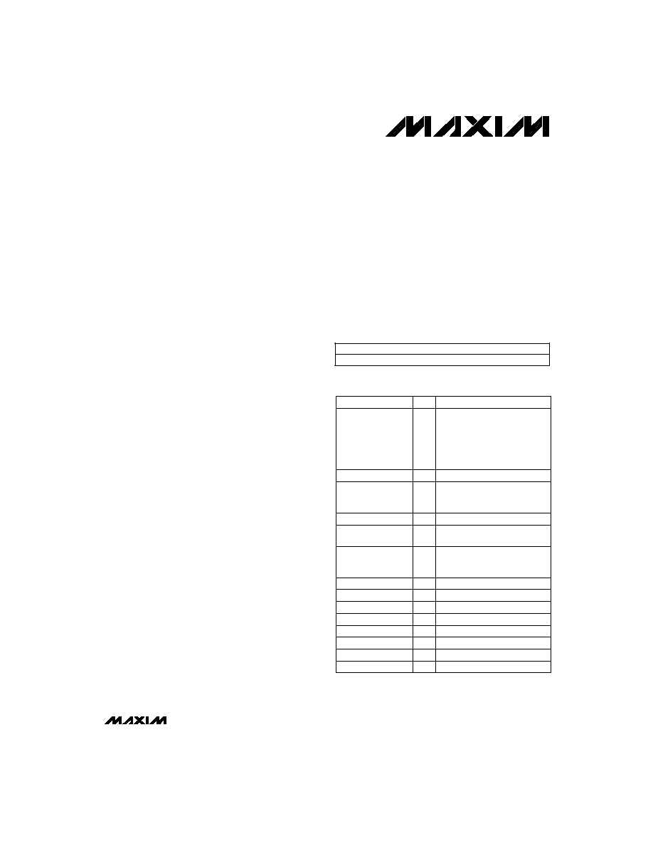
PART
TEMP. RANGE
BOARD TYPE
MAX101AEVKIT-CFR
0�C to +70�C
Surface Mount
______________Ordering Information
____________________Component List
DESIGNATION
QTY
DESCRIPTION
C1, C2, C4, C6, C7,
C9, C10, C12, C14,
C15, C18, C20, C23,
C26, C27, C29, C31,
C32, C34, C36,
C38, C40, C42
23
0.01�F capacitors
C3, C5, C11, C13
4
0.22�F capacitors
C8, C16, C30, C33,
C35, C37, C39,
C41, C43
9
100pF capacitors
C17, C21, C24
3
0.1�F capacitors
C19, C22, C25
3
10�F capacitors,
AVX "D" tantalum
D1�D4
4
100mA Schottky diodes,
Central Semiconductor
CMPSH-3
DIV 10
1
3-pin jumper block
J1, J2, J3
3
Female SMA connectors
J5
1
96-pin EURO-style plug
L1, L2
2
Ferrite beads
R1, R12
2
180
, 1% resistors
R2, R13, R23
3
121
, 1% resistors
R3, R4, R14, R15
4
100
trim pots
R5, R16, R38, R39
4
51
, 5% resistors
Component List continued on next page.

Evaluates: MAX101/MAX101A
MAX101A Evaluation Kit
2
_______________________________________________________________________________________
_________________________Quick Start
1)
Plug the termination board into the 96-pin connec-
tor of the MAX101A main board.
2)
Use a fan to provide at least 200 lineal feet/min air-
flow to the heatsink of the MAX101A.
3)
Connect the power supplies. The power-supply
input pads are in the lower right-hand corner of the
MAX101A main board. The board requires a 20W
power supply that provides +5V and -5.2V with a
common ground.
4)
Turn on the -5.2V power supply first, followed by
the +5V power supply. The -5.2V power supply
should be the first supply turned on and the last
supply turned off.
5)
Connect a low-phase-jitter RF source with a level
range of -4dBm to +10dBm to the clock input.
6)
Connect a test signal to the analog inputs. Use
IN+ and IN- if the signal is differential, or IN+ if the
signal is single-ended (�270mV (MAX101),
�250mV (MAX101A) differential; see the MAX101
or MAX101A data sheet).
7)
Observe the digitized results on the termination
board pins by using a logic analyzer, such as the
HP16500 series or an equivalent data-acquisition
system. The outputs are 100k ECL compatible.
_______________Detailed Description
Board Set
The MAX101A EV kit is a two-board set. The main board
contains ECL-interface circuitry and the MAX101A ADC.
The termination board provides high-speed signal termi-
nation and access to the digital data. For further signal
processing, the main board can be plugged into a larger
system board via the provided EURO-card connector.
Clock Input
The external clock input is capacitively coupled to an on-
board bias network. Take care to ensure that the pulse
width is within the specified requirements: clock input
levels should be -4dBm to +10dBm, and clock frequency
can range from 250MHz to 500MHz. Figure 1 in the
MAX101A data sheet shows the necessary timing
requirements for the clock input, as well as the
expected output clock waveforms. The clock input
should be driven by a low-jitter RF signal source. Refer
to Figures 1, 2, and 3 of the MAX101A data sheet for
more information.
Analog Input
Analog input to the MAX101A is made through one or
both of the two SMA coaxial connectors provided (AIN+
and AIN- inputs). Each input is a direct connection to the
ADC, with internal 50
terminations provided by the
MAX101A.
Outputs
The MAX101A main board has two 8-bit-wide digital
outputs that are 100k ECL compatible. Each data out-
put is buffered by 100E116 line receivers. There is also
a data clock output (DCLK) provided for timing. All 17
outputs provided to the EURO-card connector are dif-
ferential and unterminated.
The termination board provides a termination for each
data line, through 50
to -2V.
ADC Reference Resistor String
An on-board reference supply and op-amp circuit drive
the ADC reference resistor string. The reference sup-
plies can be adjusted using the four potentiometers on
the board (see the
Calibration Procedure). It is impor-
tant to ensure that a reverse bias condition never occurs
on the reference inputs. Schottky diode clamps on the
reference amp outputs help protect the MAX101A.
DIV 10
The jumper DIV 10 selects the operating mode of the
MAX101A, which can output data either at full speed or
at 1/10 the clock rate. This feature is valuable during
initial testing. DIV 10 is usually left open for normal (full-
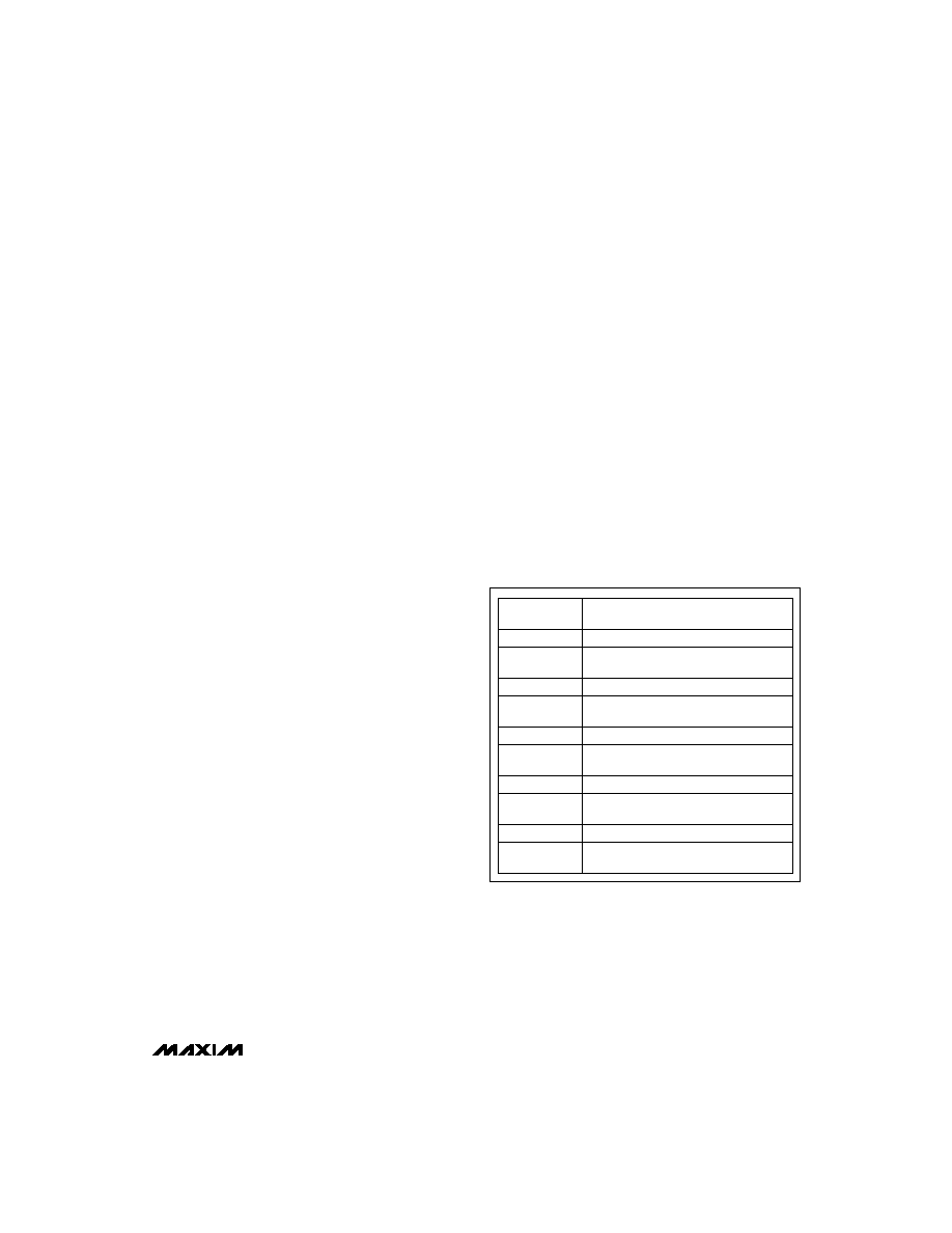
DESIGNATION
QTY
DESCRIPTION
_______Component List (continued)
R6, R7, R17, R18
4
20
, 5% resistors
R8, R9, R19, R20
4
12.1k
, 1% resistors
R10, R11, R21, R22
4
27.4
, 1% resistors
R24, R34, R36
3
82.5
, 1% resistors
R25
1
1k
, 1% resistor
R26
1
2k
trim pot
R27
1
3.16k
, 1% resistor
R28, R29, R40�R55
18
100
, 5% resistors
R35, R37
2
221
, 1% resistors
U1
1
Maxim MAX101ACFR
U2, U4
2
Maxim MAX412CPA high-
speed dual op amps
U3, U5
2
Maxim MX580KH 2.5V
references
U6
1
LM337T negative voltage
regulator
U8, U21�U24
5
MC100E116 quintuple line
receivers
speed) operation.
Power Supplies
The following supplies are required for normal opera-
tion of the main board:
V
CC
= +5V at 0.8A
V
EE
and V
AA
= -5.2V at 2.5A
These voltages should be supplied to the connector pins
for V
CC
, V
EE
, and V
AA
, respectively. V
EE
and V
AA
are
connected on the board with a ferrite bead. If system
noise must be reduced, you may remove this bead and
then provide the analog supply, V
AA
, separately from the
digital supply, V
EE
. The -5.2V power supply should be the
first supply turned on and the last supply turned off.
Board Layout
The MAX101A requires proper PC board layout for
device operation. This section explains the layout
requirements and demonstrates how the EV kit
achieves these goals.
Use power and ground planes to deliver power to the
device, keeping the digital planes separate from the
analog planes. The EV kit uses layers 3, 4, and 5 for
power and ground planes. Tie digital ground and ana-
log ground to a single point, as close to the power sup-
ply as possible. On the EV kit, digital ground ties to ana-
log ground at ferrite bead L1. Likewise, tie digital power
(V
EE
) and analog power (V
AA
) to a single point, as close
to the power supply as possible. On the EV kit, digital
power ties to analog -5.2V power at ferrite bead L2.
Use transmission lines for the analog input, clocks, and
high-speed digital outputs. The MAX101A EV kit uses
microstrip lines of two different impedances. The
MAX101A data outputs drive differential line drivers
through 100
microstrip lines. The 50
microstrip lines
occupy layers 1 and 2. The 100
microstrip lines occu-
py layers 1 and 3, with layer 2 void. The kit uses FR4
epoxy dielectric material, whose relative dielectric con-
stant is between 4.1 and 4.9. The nominal design is
0.0014 inch (0.0355mm) foil thickness for each copper
layer, and 0.011 inch (0.28mm) dielectric thickness
between layers. The 50
microstrip lines have a signal
trace width of 0.020 inch (0.50mm), and the 100
microstrip lines have a signal trace width of 0.010 inch
(0.25mm). Refer to Motorola's MECL or ECLinPS data
book for an introduction to interconnect design.
Due to the high-speed nature of this part, the propaga-
tion delay of the PC board traces becomes a significant
design consideration. For the EV kit design, the propa-
gation delay is approximately 145ps per inch
(5.7ps/mm). For best results, try to match the lengths of
the data traces to within 0.5 inch (12mm). The clock
signal must be routed on one layer only, without using
any through-hole vias. The MAX101A EV kit is a con-
trolled impedance board (50
and 100
) and has a
total board thickness of 0.062 inches (1.57mm) using
six copper layers (see Figure 1, the Layer Profile).
Evaluating the MAX101
The MAX101A EV kit also can be used to evaluate
the MAX101.
To use the MAX101, refer to specific instructions in the
Quick Start, Applications Information, and Calibration
Procedure sections.
Evaluates: MAX101/MAX101A
MAX101A Evaluation Kit
_______________________________________________________________________________________
3
Copper Layer 1
Copper thickness = 0.0007" (
1
/
2
oz
copper) (microstrip signals)
Epoxy FR4
Dielectric layer thickness = 0.011"
Copper Layer 2
Copper thickness = 0.0014" (1 oz copper)
(50
microstrip return; ground plane)
Epoxy FR4
Dielectric layer thickness = 0.011"
Copper Layer 3
Copper thickness = 0.0014" (1 oz copper)
(100
microstrip return; ground plane)
Epoxy FR4
Dielectric layer thickness = 0.011"
Copper Layer 4
Copper thickness = 0.0014" (1 oz copper)
(V
CC
/V
TT
power plane)
Epoxy FR4
Dielectric layer thickness = 0.011"
Copper Layer 5
Copper thickness = 0.0014" (1 oz copper)
(V
EE
/V
AA
power plane)
Epoxy FR4
Dielectric layer thickness = 0.011"
Copper Layer 6
Copper thickness = 0.0014" (1 oz copper)
(DC signal layer)
Figure 1. MAX101A Evaluation Board Layer Thickness Profile
__________Applications Information
Analog Input
The main board digitizes single-ended signals by choos-
ing either input and leaving the other input either open or
terminated in the system characteristic impedance. In this
mode the unused input can provide a DC offset to the
incoming signal. (See the
Electrical Characteristics in the
MAX101A data sheet for this DC voltage range.)
To obtain a digital output of all ones (11....1) with differen-
tial input drive for the MAX101, 270mV must be applied
between AIN+ and AIN-. That is, AIN+ = +135mV and
AIN- = -135mV (when no DC offset is applied). Mid-scale
digital output code occurs when there is no voltage differ-
ence across the analog inputs. Zero-scale digital output
code, with differential drive for the MAX101, occurs when
AIN+ = -135mV and AIN- = +135mV. The output of the
converter stays at all ones (full scale) or all zeros (zero
scale) when overranged or underranged, respectively.
Tables 1a and 1b show these relationships for both the
MAX101 and the MAX101A.
Digital Outputs
Data from the ADC is interleaved and is output on alter-
nate clock phases. One 8-bit word is output during one
clock phase and the other is output on the alternate clock
phase. The two 8-bit-wide data paths are buffered by
100E116 line receivers, which provide a differential output,
available at the connector. If the termination board is not
used, the user must provide proper ECL termination at the
EURO-card connector.
Input Reference-Resistor Strings
Operational amplifiers are used to drive the top and
bottom inputs of each of the ADC reference resistor
chains. A 2.5V reference is resistor-divided down
and buffered through two MAX412CPA op amps. (The
relatively low input impedance of each string, 120
,
will draw approximately 17mA.) The reference voltage
is set at the factory for either the MAX101 or MAX101A.
This reference controls the comparator input windows,
and can be adjusted between �1.20V to accommodate
input requirements. (Accuracy specifications are
guaranteed with a reference of �1.02V (MAX101) or
�0.95V (MAX101A).)
Testing
We recommend that a digital acquisition instrument like
the HP16500 series of logic analyzers be used to
acquire and process the output data. At Maxim, the
data acquired from the converter is evaluated in an
effective-bits software program developed in-house.
The effective-bits measurement is a good tool to deter-
mine and compare ADC accuracy. See the MAX101A
data sheet for more details on effective-bits testing.
_____________Calibration Procedure
The MAX101 EV kit comes calibrated and ready to
operate from the factory. If other MAX101A devices are
to be used in the same fixture, the EV kit should be
recalibrated according to the following procedure:
1)
With the ADC removed, adjust the +5V and -5.2V
power supplies.
2)
Adjust the PHASE potentiometer (R26) to a nomi-
nal voltage of 0V. A test point (TP1) for this voltage
measurement is located near the potentiometer.
3)
With the power off, insert the MAX101A into the
board. The device's heatsink fits down through the
board, and its leads rest on top of the board. Take
care to place the part in the board with Pin 1 in the
correct location. Pin 1 is indicated by a small dot
near the U1 device designation.
4)
Turn the power on, observing proper sequencing,
and let the part warm up for several minutes.
Use a fan to ensure 200 lineal feet/min airflow.
Repeat Step 2.
Evaluates: MAX101/MAX101A
MAX101A Evaluation Kit
4
_______________________________________________________________________________________
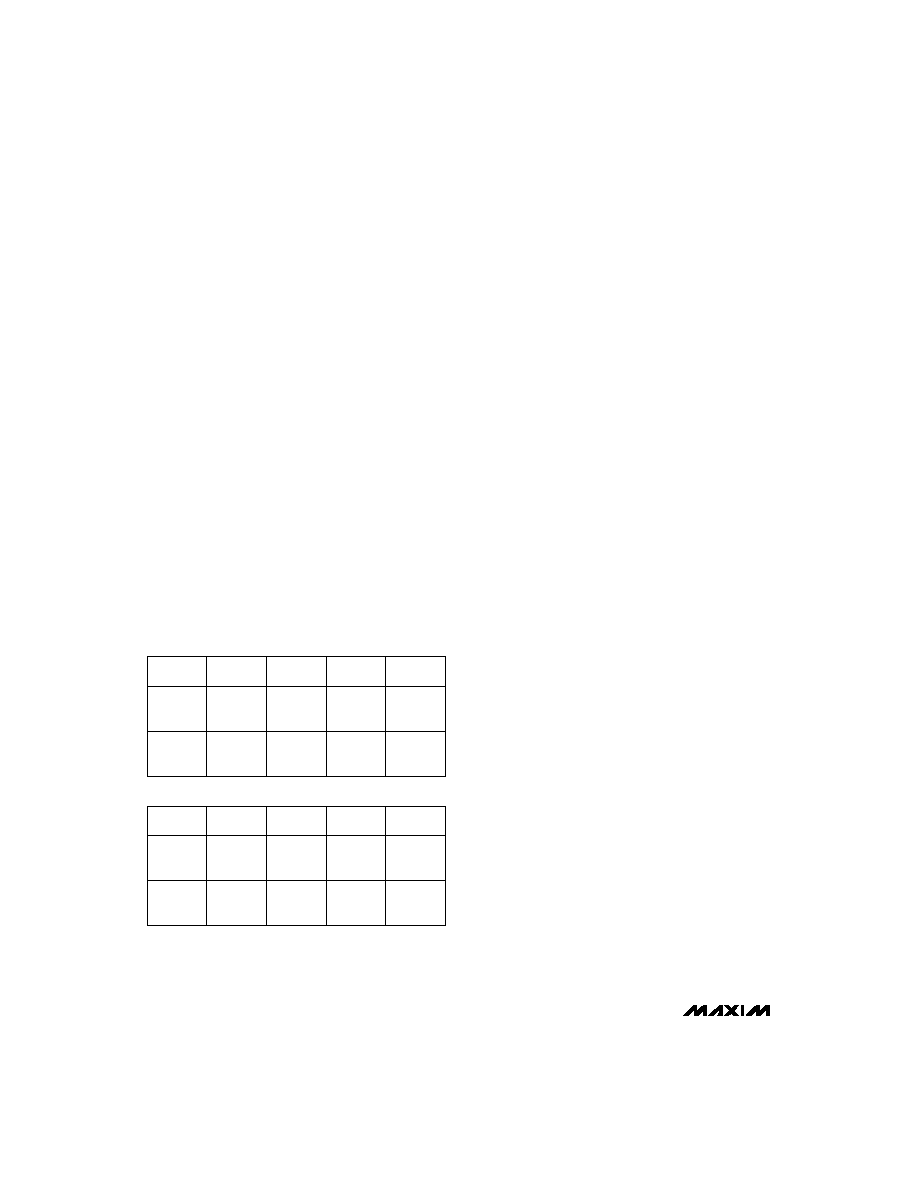
*An offset V
IO
, as specified in the
DC Electrical Characteristics,
will be present at the input. Compensate for this offset by either
adjusting the reference voltages VA
RT
, VA
RB
, VB
RT
,VB
RB
,
or introduce an offset voltage in one of the input terminals,
AIN+ or AIN-.
Table 1a. MAX101 Input Voltage Range
Table 1b. MAX101A Input Voltage Range
AIN+*
AIN-*
OUTPUT
CODE
MSB TO
LSB
INPUT
Differential
+135mV
0
-135mV
-135mV
0
+135mV
11111111
10000000
00000000
full scale
mid scale
zero scale
Single
Ended
+270mV
0
-270mV
0
0
0
11111111
10000000
00000000
full scale
mid scale
zero scale
full scale
mid scale
zero scale
AIN+*
AIN-*
OUTPUT
CODE
MSB TO
LSB
INPUT
Differential
+125mV
0
-125mV
-125mV
0
+125mV
11111111
10000000
00000000
full scale
mid scale
zero scale
Single
Ended
+250mV
0
-250mV
0
0
0
11111111
10000000
00000000
5)
After the part has warmed up for several minutes,
adjust the reference voltages to the values shown
in Tables 2a and 2b. These tables list the refer-
ence voltages, the trim pots that control the refer-
ence voltages, and the measurement points.
6)
Adjust the A converter mid-code level. With no
analog input (AIN+ - (AIN-) = 0V), the output code
should match that specified in Table 1. If there is
an offset, adjust either the positive or negative
reference (R3 or R4) until the expected code of
10 00 00 00 (MSB to LSB) is achieved. After
adjusting to the proper level, the references need
to be balanced to the proper values shown in
Tables 2a and 2b, around any offset that was
introduced. (If the negative reference was moved
by +32mV, the positive reference must be moved
by that same amount to ensure the correct LSB
size.) It may be necessary to repeat the reference
offset adjustment again after the correct differen-
tial reference voltage is re-established around a
common-mode offset.
7)
Repeat Step 6 for the B converter reference volt-
ages. (The adjustment pots of the B converter are
R14 and R15.)
8)
Adjust the phase potentiometer (R26) for best
effective bits performance (optional). While digitiz-
ing a pure sine-wave input, compute the effective-
bits performance of the interleaved output data.
Good performance can be achieved with the
PH
ADJ
voltage set to 0V (Step 2); however, maxi-
mum performance can be achieved by adjusting
the sampling delay with R26 as required.
Evaluates: MAX101/MAX101A
MAX101A Evaluation Kit
_______________________________________________________________________________________
5
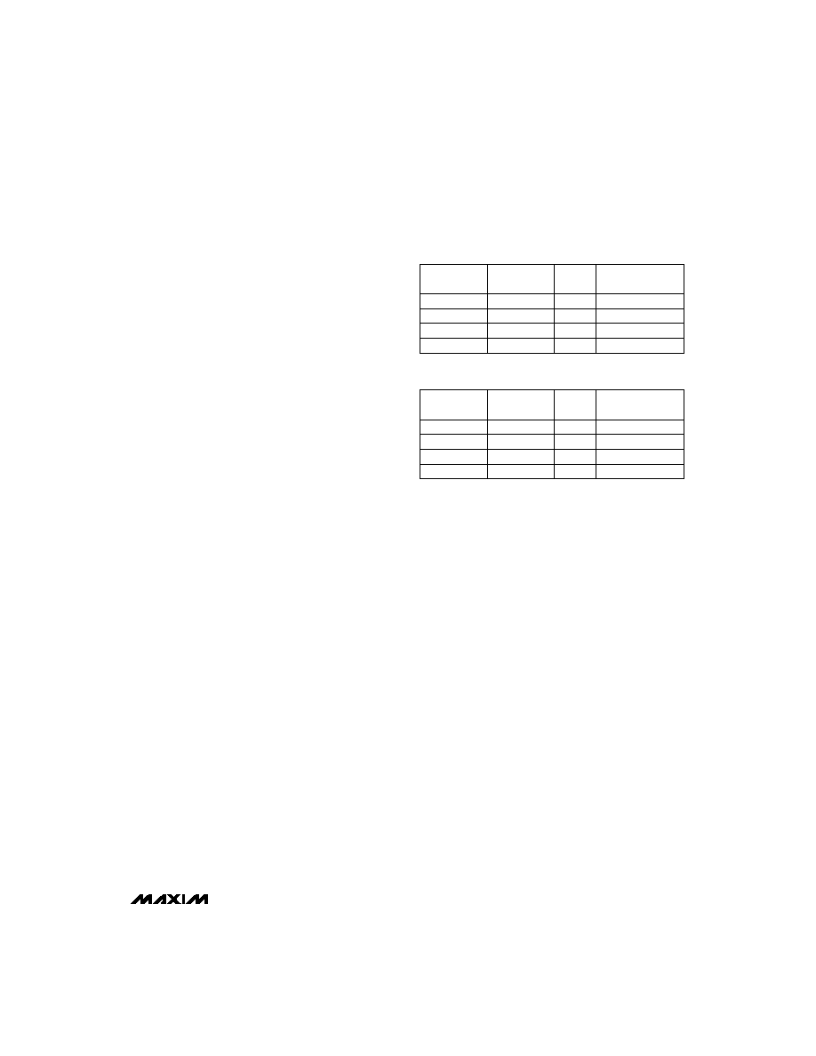
Table 2a. MAX101 Reference Adjustments
REFERENCE
VOLTAGE
TRIM
POT
MEASURE AT
DEVICE SIDE OF:
+1.02V
R3
R5
-1.02V
R4
R8
+1.02V
R14
R16
-1.02V
R15
R19
CONVERTER
A
A
B
B
Table 2b. MAX101A Reference Adjustments
CONVERTER
A
A
REFERENCE
VOLTAGE
TRIM
POT
MEASURE AT
DEVICE SIDE OF:
+0.95V
R3
R5
-0.95V
R4
R8
+0.95V
R14
R16
-0.95V
R15
R19
B
B