 | ÐлекÑÑоннÑй компоненÑ: MAX1035 | СкаÑаÑÑ:  PDF PDF  ZIP ZIP |
Äîêóìåíòàöèÿ è îïèñàíèÿ www.docs.chipfind.ru
General Description
The MAX1034/MAX1035 multirange, low-power, 14-bit,
successive-approximation, analog-to-digital converters
(ADCs) operate from a single +5V supply and achieve
throughput rates up to 115ksps. A separate digital sup-
ply allows digital interfacing with 2.7V to 5.25V systems
using the SPITM-/QSPITM-/MICROWIRETM-compatible
serial interface. Partial power-down mode reduces the
supply current to 1.3mA (typ). Full power-down mode
reduces the power-supply current to 1µA (typ).
The MAX1034 provides eight (single-ended) or four (true
differential) analog input channels. The MAX1035 pro-
vides four (single-ended) or two (true differential) analog
input channels. Each analog input channel is indepen-
dently software programmable for seven single-ended
input ranges (0 to +V
REF
/2, -V
REF
/2 to 0, 0 to +V
REF
,
-V
REF
to 0, ±V
REF
/4, ±V
REF
/2, and ±V
REF
), and three
differential input ranges (±V
REF
/2, ±V
REF
, ±2 x V
REF
).
An on-chip +4.096V reference offers a small convenient
ADC solution. The MAX1034/MAX1035 also accept an
external reference voltage between 3.800V and 4.136V.
The MAX1034 is available in a 24-pin TSSOP package
and the MAX1035 is available in a 20-pin TSSOP pack-
age. Each device is specified for operation from -40°C
to +85°C.
Applications
Industrial Control Systems
Data-Acquisition Systems
Avionics
Robotics
Features
Software-Programmable Input Range for Each
Channel
Single-Ended Input Ranges
0 to +V
REF
/2, -V
REF
/2 to 0, 0 to +V
REF
, -V
REF
to
0, ±V
REF
/4, ±V
REF
/2, and ±V
REF
Differential Input Ranges
±V
REF
/2, ±V
REF
, and ±2 x V
REF
Eight Single-Ended or Four Differential Analog
Inputs (MAX1034)
Four Single-Ended or Two Differential Analog
Inputs (MAX1035)
±6V Overvoltage Tolerant Inputs
Internal or External Reference
115ksps Maximum Sample Rate
Single +5V Power Supply
20-/24-Pin TSSOP Package
MAX1034/MAX1035
8-/4-Channel, ±V
REF
Multirange Inputs,
Serial 14-Bit ADCs
________________________________________________________________ Maxim Integrated Products
1
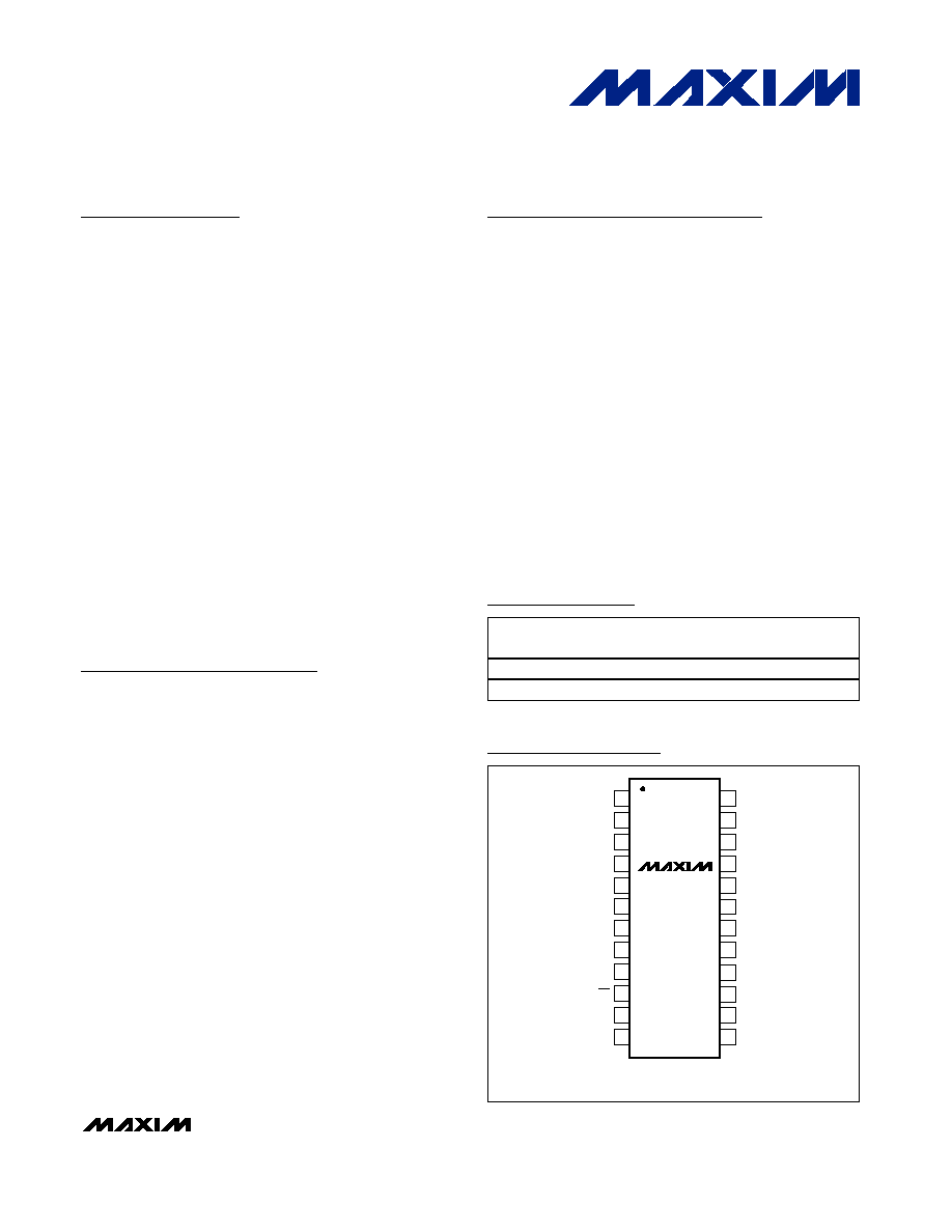
Pin Configurations
Ordering Information
24
23
22
21
20
19
18
17
1
2
3
4
5
6
7
8
AGND1
AGND2
AV
DD2
AGND3
CH2
CH1
CH0
AV
DD1
TOP VIEW
REF
REFCAP
DV
DD
DV
DDO
CH6
CH5
CH4
CH3
16
15
14
13
9
10
11
12
DGND
DGNDO
DOUT
SCLK
SSTRB
DIN
CS
CH7
TSSOP
MAX1034
19-3574; Rev 0; 5/05
For pricing, delivery, and ordering information, please contact Maxim/Dallas Direct! at
1-888-629-4642, or visit Maxim's website at www.maxim-ic.com.
PART
TEMP RANGE
PIN-
PACKAGE
CHANNELS
MAX1034EUG*
-40°C to +85°C
24 TSSOP
8
MAX1035EUP
-40°C to +85°C
20 TSSOP
4
SPI and QSPI are a trademarks of Motorola, Inc.
MICROWIRE is a trademark of National Semiconductor Corp.
Pin Configurations continued at end of data sheet.
*Future product--contact factory for availability.
MAX1034/MAX1035
8-/4-Channel, ±V
REF
Multirange Inputs,
Serial 14-Bit ADCs
2
_______________________________________________________________________________________
ABSOLUTE MAXIMUM RATINGS
ELECTRICAL CHARACTERISTICS
(AV
DD1
= AV
DD2
= DV
DD
= DV
DDO
= 5V, AGND1 = DGND = DGNDO = AGND2 = AGND3 = 0, f
CLK
= 3.5MHz (50% duty cycle), external
clock mode, V
REF
= 4.096V (external reference operation), REFCAP = AV
DD1
, maximum single-ended bipolar input range (±V
REF
), C
DOUT
= 50pF, C
SSTRB
= 50pF, T
A
= -40°C to +85°C, unless otherwise noted. Typical values are at T
A
= +25°C.)
Stresses beyond those listed under "Absolute Maximum Ratings" may cause permanent damage to the device. These are stress ratings only, and functional
operation of the device at these or any other conditions beyond those indicated in the operational sections of the specifications is not implied. Exposure to
absolute maximum rating conditions for extended periods may affect device reliability.
AVDD1 to AGND1 ....................................................-0.3V to +6V
AVDD2 to AGND2 ....................................................-0.3V to +6V
DVDD to DGND ........................................................-0.3V to +6V
DVDDO to DGNDO ..................................................-0.3V to +6V
DVDD to DVDDO......................................................-0.3V to +6V
DVDD, DVDDO to AVDD1 ........................................-0.3V to +6V
AVDD1, DVDD, DVDDO to AVDD2 ..........................-0.3V to +6V
DGND, DGNDO, AGND3, AGND2 to AGND1 ......-0.3V to +0.3V
CS, SCLK, DIN, DOUT, SSTRB to
DGNDO ............................................-0.3V to (DVDDO + 0.3V)
CH0CH7 to AGND1 ...................................................-6V to +6V
REF, REFCAP to AGND1.......................-0.3V to (AVDD1 + 0.3V)
Continuous Current (any pin) ...........................................±50mA
Continuous Power Dissipation (T
A
= +70°C)
20-Pin TSSOP (derate 11mW/°C above +70°C) ..........879mW
24-Pin TSSOP (derate 12.2mW/°C above +70°C) .......976mW
Operating Temperature Range ...........................-40°C to +85°C
Junction Temperature .....................................................+150°C
Storage Temperature Range .............................-65°C to +150°C
Lead Temperature (soldering, 10s) .................................+300°C
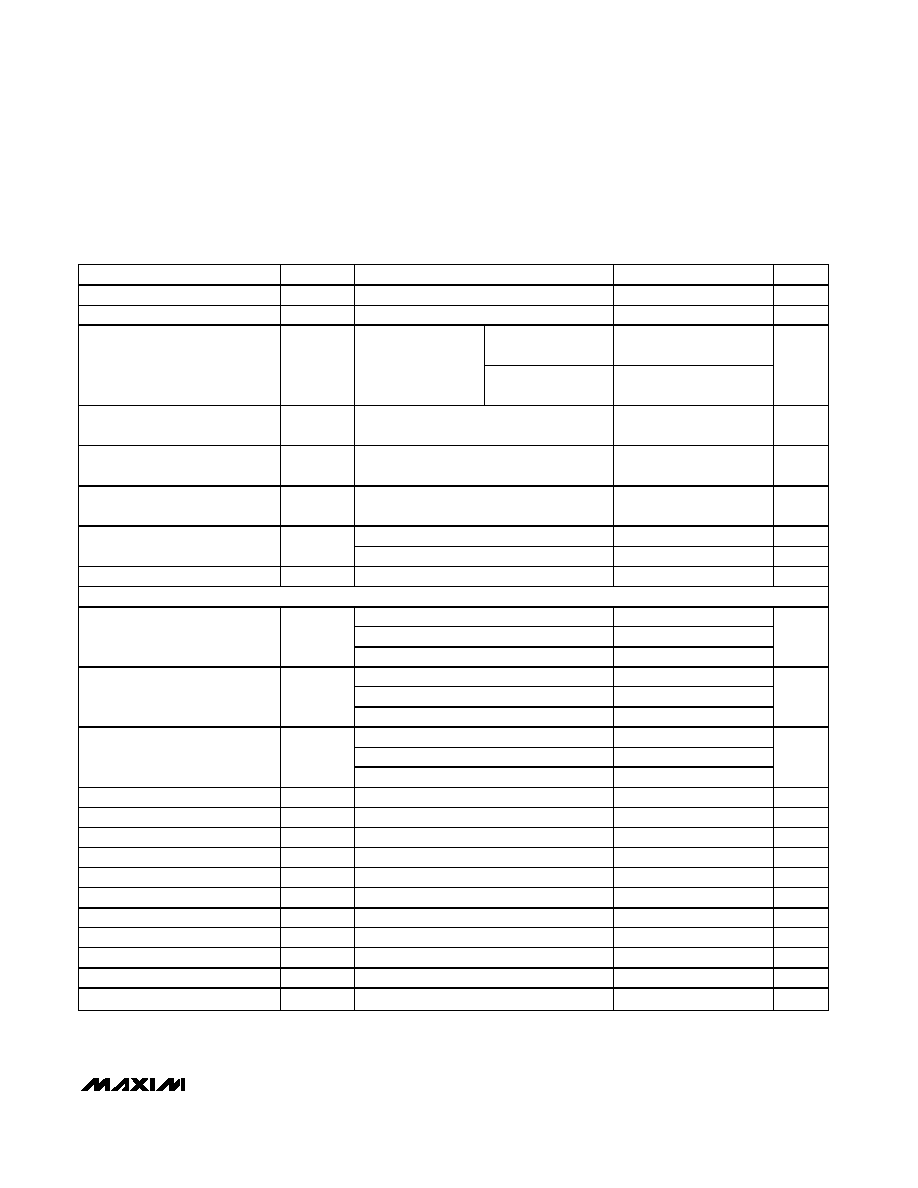
PARAMETER
SYMBOL
CONDITIONS
MIN
TYP
MAX
UNITS
DC ACCURACY (Notes 1, 2)
Resolution
14
Bits
Integral Nonlinearity
INL
±0.25
±1
LSB
Differential Nonlinearity
DNL
No missing codes
±1
LSB
0.5
Transition Noise
External or internal reference
2
LSB
RMS
Unipolar
0
±10
Single-ended inputs
Bipolar
-1.0
±10
Unipolar
0
±20
Offset Error
Differential inputs
(Note 3)
Bipolar
-2
±20
mV
Channel-to-Channel Gain
Matching
Unipolar or bipolar
0.025
%FSR
Channel-to-Channel Offset Error
Matching
Unipolar or bipolar
1.0
mV
Unipolar
10
Offset Temperature Coefficient
Bipolar
5
ppm/°C
Unipolar
±0.5
Gain Error
Bipolar
±0.3
%FSR
Unipolar
1.5
Gain Temperature Coefficient
Bipolar
1.0
ppm/°C
Unipolar Endpoint Overlap
Negative unipolar full scale to positive
unipolar zero-scale
0
5
LSB
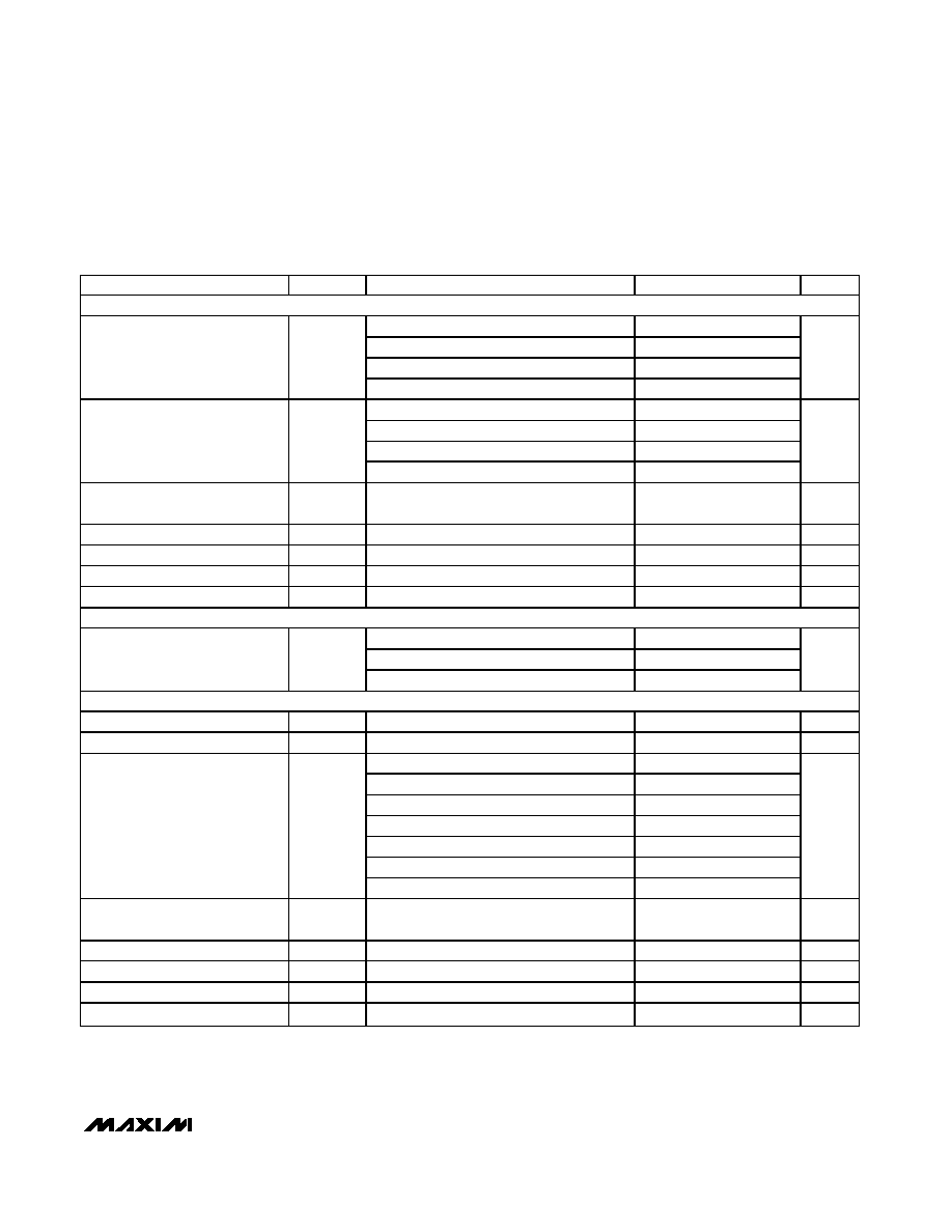
MAX1034/MAX1035
8-/4-Channel, ±V
REF
Multirange Inputs,
Serial 14-Bit ADCs
_______________________________________________________________________________________
3
PARAMETER
SYMBOL
CONDITIONS
MIN
TYP
MAX
UNITS
DYNAMIC SPECIFICATIONS f
IN(SINE-WAVE)
= 5kHz, V
IN
= FSR - 0.05dB, f
SAMPLE
= 130ksps (Notes 1, 2)
Differential inputs, FSR = 2 x V
REF
84.5
Single-ended inputs, FSR = V
REF
84
Single-ended inputs, FSR = V
REF
/ 2
82.5
Signal-to-Noise Plus Distortion
SINAD
Single-ended inputs, FSR = V
REF
/ 4
79
80.5
dB
Differential inputs, FSR = 2 x V
REF
84.5
Single-ended inputs, FSR = V
REF
84
Single-ended inputs, FSR = V
REF
/ 2
82.5
Signal-to-Noise Ratio
SNR
Single-ended inputs, FSR = V
REF
/ 4
80.5
dB
Total Harmonic Distortion
(Up to the 5th Harmonic)
THD
-98
dB
Spurious-Free Dynamic Range
SFDR
92
99
dB
Aperture Delay
t
AD
Figure 21
15
ns
Aperture Jitter
t
AJ
Figure 21
100
ps
Channel-to-Channel Isolation
105
dB
CONVERSION RATE
External clock mode, Figure 2
114
External acquisition mode, Figure 3
84
Byte-Wide Throughput Rate
f
SAMPLE
Internal clock mode, Figure 4
106
ksps
ANALOG INPUTS (CH0CH3 MAX1035, CH0CH7 MAX1034, AGND1)
Small-Signal Bandwidth
All input ranges, V
IN
= 100mV
P-P
(Note 2)
2
MHz
Full-Power Bandwidth
All input ranges, V
IN
= 4V
P-P
(Note 2)
700
kHz
R[2:1] = 001
-V
REF
/4
+V
REF
/4
R[2:1] = 010
-V
REF
/2
0
R[2:1] = 011
0
+V
REF
/2
R[2:1] = 100
-V
REF
/2
+V
REF
/2
R[2:1] = 101
-V
REF
0
R[2:1] = 110
0
+V
REF
Input Voltage Range (Table 6)
V
CH_
R[2:1] = 111
-V
REF
+V
REF
V
True-Differential Analog
Common-Mode Voltage Range
V
CMDR
DIF/SGL = 1
-4.75
+5.50
V
Common-Mode Rejection Ratio
CMRR
DIF/SGL = 1, input voltage range = ±V
REF
/4
75
dB
Input Current
I
CH_
-V
REF
< V
CH_
< +V
REF
-1500
+650
µA
Input Capacitance
C
CH_
5
pF
Input Resistance
R
CH_
6
k
ELECTRICAL CHARACTERISTICS (continued)
(AV
DD1
= AV
DD2
= DV
DD
= DV
DDO
= 5V, AGND1 = DGND = DGNDO = AGND2 = AGND3 = 0, f
CLK
= 3.5MHz (50% duty cycle), external
clock mode, V
REF
= 4.096V (external reference operation), REFCAP = AV
DD1
, maximum single-ended bipolar input range (±V
REF
), C
DOUT
= 50pF, C
SSTRB
= 50pF, T
A
= -40°C to +85°C, unless otherwise noted. Typical values are at T
A
= +25°C.)
MAX1034/MAX1035
8-/4-Channel, ±V
REF
Multirange Inputs,
Serial 14-Bit ADCs
4
_______________________________________________________________________________________
PARAMETER
SYMBOL
CONDITIONS
MIN
TYP
MAX
UNITS
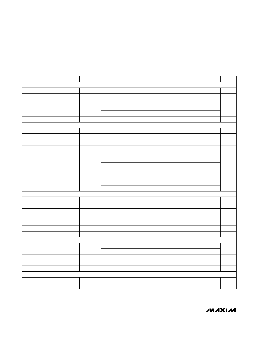
INTERNAL REFERENCE (Bypass REFCAP with 0.1µF to AGND1 and REF with 1.0µF to AGND1)
Reference Output Voltage
V
REF
4.056
4.096
4.136
V
Reference Temperature
Coefficient
TC
REF
±30
ppm/°C
REF shorted to AGND1
10
Reference Short-Circuit Current
I
REFSC
REF shorted to AV
DD
-1
mA
Reference Load Regulation
I
REF
= 0 to 0.5mA
0.1
10
mV
EXTERNAL REFERENCE (REFCAP = AV
DD
)
Reference Input Voltage Range
V
REF
3.800
4.136
V
REFCAP Buffer Disable
Threshold
V
RCTH
(Note 4)
AV
DD1
- 0.4
AV
DD1
- 0.1
V
V
REF
= +4.096V, external clock mode,
external acquisition mode, internal clock
mode, or partial power-down mode
90
200
Reference Input Current
I
REF
V
REF
= +4.096V, full power-down mode
±0.1
±10
µA
External clock mode, external acquisition
mode, internal clock mode, or partial
power-down mode
20
45
Reference Input Resistance
R
REF
Full power-down mode
40
k
DIGITAL INPUTS (DIN, SCLK, CS)
Input High Voltage
V
IH
0.7 x
DV
DDO
V
Input Low Voltage
V
IL
0.3 x
DV
DDO
V
Input Hysteresis
V
HYST
0.2
V
Input Leakage Current
I
IN
V
IN
= 0 to DV
DDO
-10
+10
µA
Input Capacitance
C
IN
10
pF
DIGITAL OUTPUTS (DOUT, SSTRB)
DV
DDO
= 4.75V, I
SINK
= 10mA
0.4
Output Low Voltage
V
OL
DV
DDO
= 2.7V, I
SINK
= 5mA
0.4
V
Output High Voltage
V
OH
I
SOURCE
= 0.5mA
DV
DDO
- 0.4
V
DOUT Tri-State Leakage Current
I
DDO
CS = DV
DDO
-10
+10
µA
POWER REQUIREMENTS (AV
DD1
and AGND1, AV
DD2
and AGND2, DV
DD
and DGND, DV
DDO
and DGNDO)
Analog Supply Voltage
AV
DD1
4.75
5.25
V
Digital Supply Voltage
DV
DD
4.75
5.25
V
ELECTRICAL CHARACTERISTICS (continued)
(AV
DD1
= AV
DD2
= DV
DD
= DV
DDO
= 5V, AGND1 = DGND = DGNDO = AGND2 = AGND3 = 0, f
CLK
= 3.5MHz (50% duty cycle), external
clock mode, V
REF
= 4.096V (external reference operation), REFCAP = AV
DD1
, maximum single-ended bipolar input range (±V
REF
), C
DOUT
= 50pF, C
SSTRB
= 50pF, T
A
= -40°C to +85°C, unless otherwise noted. Typical values are at T
A
= +25°C.)
MAX1034/MAX1035
8-/4-Channel, ±V
REF
Multirange Inputs,
Serial 14-Bit ADCs
_______________________________________________________________________________________
5
PARAMETER
SYMBOL
CONDITIONS
MIN
TYP
MAX
UNITS
Preamplifier Supply Voltage
AV
DD2
4.75
5.25
V
Digital I/O Supply Voltage
DV
DDO
2.70
5.25
V
Internal reference
3
3.5
AV
DD1
Supply Current
I
AVDD1
External clock mode,
external acquisition
mode, or internal
clock mode
External reference
2.5
3
mA
DV
DD
Supply Current
I
DVDD
External clock mode, external acquisition
mode, or internal clock mode
0.9
2
mA
AV
DD2
Supply Current
I
AVDD2
External clock mode, external acquisition
mode, or internal clock mode
17.5
25
mA
DV
DDO
Supply Current
I
DVDDO
External clock mode, external acquisition
mode, or internal clock mode
0.2
1
mA
Partial power-down mode
1.3
mA
Total Supply Current
Full power-down mode
1
µA
Power-Supply Rejection Ratio
PSRR
All analog input ranges
±0.125
LSB
TIMING CHARACTERISTICS (Figures 15 and 16)
External clock mode
272
62
External acquisition mode
228
62
SCLK Period
t
CP
Internal clock mode
100
83
µs
External clock mode
109
External acquisition mode
92
SCLK High Pulse Width (Note 5)
t
CH
Internal clock mode
40
ns
External clock mode
109
External acquisition mode
92
SCLK Low Pulse Width (Note 5)
t
CL
Internal clock mode
40
ns
DIN to SCLK Setup
t
DS
40
ns
DIN to SCLK Hold
t
DH
0
ns
SCLK Fall to DOUT Valid
t
DO
40
ns
CS Fall to DOUT Enable
t
DV
40
ns
CS Rise to DOUT Disable
t
TR
40
ns
CS Fall to SCLK Rise Setup
t
CSS
40
ns
CS High Minimum Pulse Width
t
CSPW
40
ns
SCLK Fall to CS Rise Hold
t
CSH
0
ns
SSTRB Rise to CS Fall Setup
40
ns
DOUT Rise/Fall Time
C
L
= 50pF
10
ns
SSTRB Rise/Fall Time
C
L
= 50pF
10
ns
ELECTRICAL CHARACTERISTICS (continued)
(AV
DD1
= AV
DD2
= DV
DD
= DV
DDO
= 5V, AGND1 = DGND = DGNDO = AGND2 = AGND3 = 0, f
CLK
= 3.5MHz (50% duty cycle), external
clock mode, V
REF
= 4.096V (external reference operation), REFCAP = AV
DD1
, maximum single-ended bipolar input range (±V
REF
), C
DOUT
= 50pF, C
SSTRB
= 50pF, T
A
= -40°C to +85°C, unless otherwise noted. Typical values are at T
A
= +25°C.)