 | ÐлекÑÑоннÑй компоненÑ: MAX1039 | СкаÑаÑÑ:  PDF PDF  ZIP ZIP |
Äîêóìåíòàöèÿ è îïèñàíèÿ www.docs.chipfind.ru
General Description
The MAX1036MAX1039 low-power, 8-bit, multichannel,
analog-to-digital converters (ADCs) feature internal
track/hold (T/H), voltage reference, clock, and an
I
2
C-compatible 2-wire serial interface. These devices
operate from a single supply and require only 350µA at
the maximum sampling rate of 188ksps. Auto-
ShutdownTM powers down the devices between conver-
sions reducing supply current to less than 1µA at low
throughput rates. The MAX1036/MAX1037 have four ana-
log input channels each, while the MAX1038/MAX1039
have twelve analog input channels. The analog inputs are
software configurable for unipolar or bipolar and single-
ended or pseudo-differential operation.
The full-scale analog input range is determined by the
internal reference or by an externally applied reference
voltage ranging from 1V to V
DD
. The MAX1037/
MAX1039 feature a 2.048V internal reference and the
MAX1036/MAX1038 feature a 4.096V internal reference.
The MAX1036/MAX1037 are available in 8-pin SOT23
packages. The MAX1038/MAX1039 are available in 16-
pin QSOP packages. The MAX1036MAX1039 are guar-
anteed over the extended industrial temperature range
(-40°C to +85°C). Refer to MAX1136MAX1139 for 10-bit
devices and to the MAX1236MAX1239 for 12-bit
devices.
Applications
Hand-Held Portable Applications
Medical Instruments
Battery-Powered Test Equipment
Solar-Powered Remote Systems
Received-Signal-Strength Indicators
System Supervision
Features
o High-Speed I
2
C-Compatible Serial Interface
400kHz Fast Mode
1.7MHz High-Speed Mode
o Single Supply
2.7V to 3.6V (MAX1037/MAX1039)
4.5V to 5.5V (MAX1036/MAX1038)
o Internal Reference
2.048V (MAX1037/MAX1039)
4.096V (MAX1036/MAX1038)
o External Reference: 1V to V
DD
o Internal Clock
o 4-Channel Single-Ended or 2-Channel Pseudo-
Differential (MAX1036/MAX1037)
o 12-Channel Single-Ended or 6-Channel Pseudo-
Differential (MAX1038/MAX1039)
o Internal FIFO with Channel-Scan Mode
o Low Power
350µA at 188ksps
110µA at 75ksps
8µA at 10ksps
1µA in Power-Down Mode
o Software Configurable Unipolar/Bipolar
o Small Packages
8-Pin SOT23 (MAX1036/MAX1037)
16-Pin QSOP (MAX1038/MAX1039)
MAX1036MAX1039
2.7V to 5.5V, Low-Power, 4-/12-Channel
2-Wire Serial 8-Bit ADCs
________________________________________________________________ Maxim Integrated Products
1
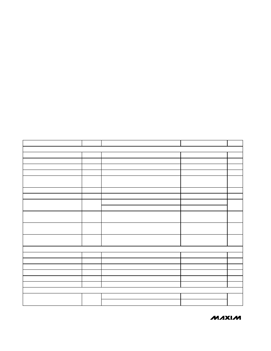
Ordering Information
19-2442; Rev 1; 10/02
For pricing, delivery, and ordering information, please contact Maxim/Dallas Direct! at
1-888-629-4642, or visit Maxim's website at www.maxim-ic.com.
PART
TEMP RANGE
PIN-PACKAGE
TUE
(LSB)
INPUT
CHANNELS
INTERNAL
REFERENCE (V)
TOP
MARK
MAX1036EKA-T
-40
°C to +85°C
8 SOT23-8
±2
4
4.096
AAJE
MAX1037EKA-T
-40
°C to +85°C
8 SOT23-8
±2
4
2.048
AAJG
MAX1038AEEE
-40
°C to +85°C
16 QSOP
±1
12
4.096
--
MAX1039AEEE
-40
°C to +85°C
16 QSOP
±1
12
2.048
--
AutoShutdown is a trademark of Maxim Integrated Products, Inc.
Pin Configurations and Typical Operating Circuit appear
at end of data sheet.
MAX1036MAX1039
2.7V to 5.5V, Low-Power, 4-/12-Channel
2-Wire Serial 8-Bit ADCs
2
_______________________________________________________________________________________
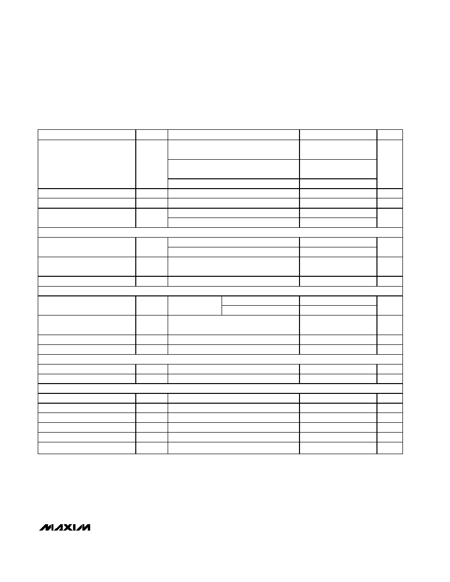
ABSOLUTE MAXIMUM RATINGS
ELECTRICAL CHARACTERISTICS
(V
DD
= 2.7V to 3.6V (MAX1037/MAX1039), V
DD
= 4.5V to 5.5V (MAX1036/MAX1038). External reference, V
REF
= 2.048V
(MAX1037/MAX1039), V
REF
= 4.096V (MAX1036/MAX1038). External clock, f
SCL
= 1.7MHz, T
A
= T
MIN
to T
MAX
, unless otherwise
noted. Typical values are at T
A
= +25°C.)
Stresses beyond those listed under "Absolute Maximum Ratings" may cause permanent damage to the device. These are stress ratings only, and functional
operation of the device at these or any other conditions beyond those indicated in the operational sections of the specifications is not implied. Exposure to
absolute maximum rating conditions for extended periods may affect device reliability.
V
DD
to GND ..............................................................-0.3V to +6V
AIN0AIN11, REF to
GND ......................-0.3V to the lower of (V
DD
+ 0.3V) and +6V
SDA, SCL to GND.....................................................-0.3V to +6V
Maximum Current Into Any Pin .........................................±50mA
Continuous Power Dissipation (T
A
= +70°C)
8-Pin SOT23 (derate 7.1mW/°C above +70°C).............567mW
16-Pin QSOP (derate 8.3mW/°C above +70°C).........666.7mW
Operating Temperature Range ...........................-40°C to +85°C
Junction Temperature ......................................................+150°C
Storage Temperature Range .............................-60°C to +150°C
Lead Temperature (soldering, 10s) .................................+300°C
PARAMETER
SYMBOL
CONDITIONS
MIN
TYP
MAX
UNITS
DC ACCURACY (Note 1)
Resolution
8
Bits
Relative Accuracy
INL
(Note 2)
±1
LSB
Differential Nonlinearity
DNL
No missing codes over temperature
±1
LSB
Offset Error
±1.5
LSB
Offset Error Temperature
Coefficient
3
ppm/
°C
Gain Error
(Note 3)
±1
LSB
Gain Temperature Coefficient
±1
ppm/
°C
MAX1036/MAX1037
±0.5
±2
Total Unadjusted Error
TUE
MAX1038A/MAX1039A
±0.5
±1
LSB
Channel-to-Channel Offset
Matching
±0.1
LSB
Channel-to-Channel Gain
Matching
±0.5
LSB
Input Common-Mode Rejection
Ratio
CMRR
Pseudo-differential input mode
75
dB
DYNAMIC PERFORMANCE (f
IN(sine wave)
= 25kHz, V
IN
= V
REF(P-P)
, f
SAMPLE
= 188ksps, R
IN
= 100
)
Signal-to-Noise Plus Distortion
SINAD
49
dB
Total Harmonic Distortion
THD
Up to the 5th harmonic
-69
dB
Spurious-Free Dynamic Range
SFDR
69
dB
Channel-to-Channel Crosstalk
(Note 4)
75
dB
Full-Power Bandwidth
-3dB point
2.0
MHz
Full-Linear Bandwidth
SINAD > 49dB
200
kHz
CONVERSION RATE
Internal clock
6.1
Conversion Time (Note 5)
t
CONV
External clock
4.7
µs
MAX1036MAX1039
2.7V to 5.5V, Low-Power, 4-/12-Channel
2-Wire Serial 8-Bit ADCs
_______________________________________________________________________________________
3
ELECTRICAL CHARACTERISTICS (continued)
(V
DD
= 2.7V to 3.6V (MAX1037/MAX1039), V
DD
= 4.5V to 5.5V (MAX1036/MAX1038). External reference, V
REF
= 2.048V
(MAX1037/MAX1039), V
REF
= 4.096V (MAX1036/MAX1038). External clock, f
SCL
= 1.7MHz, T
A
= T
MIN
to T
MAX
, unless otherwise
noted. Typical values are at T
A
= +25°C.)
PARAMETER
SYMBOL
CONDITIONS
MIN
TYP
MAX
UNITS
Internal clock, SCAN[1:0] = 01
(MAX1036/MAX1037)
76
Internal clock, SCAN[1:0] = 00
CS[3:0] = 1011 (MAX1038/MAX1039)
77
Throughput Rate
f
SAMPLE
External clock
188
ksps
Track/Hold Acquisition Time
588
ns
Internal Clock Frequency
2.25
MHz
External clock, fast mode
45
Aperture Delay
t
AD
External clock, high-speed mode
30
ns
ANALOG INPUT (AIN0AIN11)
Unipolar
0
V
REF
Input Voltage Range, Single
Ended and Differential (Note 6)
Bipolar
±V
REF
/ 2
V
Input Multiplexer Leakage Current
On/off-leakage current, V
AIN
_= 0 or V
DD,
no clock, f
SCL
= 0
±0.01
±1
µA
Input Capacitance
C
IN
18
pF
INTERNAL REFERENCE (Note 7)
MAX1037/MAX1039
1.925
2.048
2.171
Reference Voltage
V
REF
T
A
= +25°C
MAX1036/MAX1038
3.850
4.096
4.342
V
Reference Temperature
Coefficient
TC
REF
120
ppm/
°C
Reference Short-Circuit Current
10
mA
Reference Source Impedance
(Note 8)
675
EXTERNAL REFERENCE
Reference Input Voltage Range
V
REF
(Note 9)
1.0
V
DD
V
REF Input Current
I
REF
f
SAMPLE
= 188ksps
14
30
µA
DIGITAL INPUTS/OUTPUTS (SCL, SDA)
Input High Voltage
V
IH
0.7 x V
DD
V
Input Low Voltage
V
IL
0.3 x V
DD
V
Input Hysteresis
V
HYST
0.1 x V
DD
V
Input Current
I
IN
V
IN
= 0 to V
DD
±10
µA
Input Capacitance
C
IN
15
pF
Output Low Voltage
V
OL
I
SINK
= 3mA
0.4
V
MAX1036MAX1039
2.7V to 5.5V, Low-Power, 4-/12-Channel
2-Wire Serial 8-Bit ADCs
4
_______________________________________________________________________________________
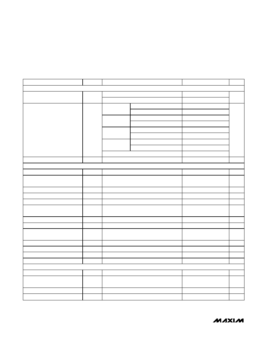
ELECTRICAL CHARACTERISTICS (continued)
(V
DD
= 2.7V to 3.6V (MAX1037/MAX1039), V
DD
= 4.5V to 5.5V (MAX1036/MAX1038). External reference, V
REF
= 2.048V
(MAX1037/MAX1039), V
REF
= 4.096V (MAX1036/MAX1038). External clock, f
SCL
= 1.7MHz, T
A
= T
MIN
to T
MAX
, unless otherwise
noted. Typical values are at T
A
= +25°C.)
PARAMETER
SYMBOL
CONDITIONS
MIN
TYP
MAX
UNITS
POWER REQUIREMENTS
MAX1037/MAX1039
2.7
3.6
Supply Voltage (Note 10)
V
DD
MAX1036/MAX1038
4.5
5.5
V
Internal REF, external clock
350
650
f
SAMPLE
=
188ksps
External REF, external clock
250
External REF, external clock
110
f
SAMPLE
=
75ksps
External REF, internal clock
150
External REF, external clock
8
f
SAMPLE
=
10ksps
External REF, internal clock
10
External REF, external clock
2
f
SAMPLE
=
1ksps
External REF, internal clock
2.5
Supply Current
I
DD
Power-down
1
10
µA
Power-Supply Rejection Ratio
PSRR
(Note 11)
±0.25
±1
LSB/V
TIMING CHARACTERISTICS FOR 2-WIRE FAST MODE (Figures 1A and 2)
Serial Clock Frequency
f
SCL
400
kHz
Bus Free Time Between a STOP
and a START Condition
t
BUF
1.3
µs
Hold Time for Start Condition
t
HD,
STA
0.6
µs
Low Period of the SCL Clock
t
LOW
1.3
µs
High Period of the SCL Clock
t
HIGH
0.6
µs
Setup Time for a Repeated START
Condition (Sr)
t
SU,
STA
0.6
µs
Data Hold Time
t
HD,
DAT
(Note 12)
0
150
ns
Data Setup Time
t
SU,
DAT
100
ns
Rise Time of Both SDA and SCL
Signals, Receiving
t
R
(Note 13)
20 + 0.1C
B
300
ns
Fall Time of SDA Transmitting
t
F
(Note 13)
20 + 0.1C
B
300
ns
Setup Time for STOP Condition
t
SU,
STO
0.6
µs
Capacitive Load for Each Bus Line
C
B
400
pF
Pulse Width of Spike Suppressed
t
SP
50
ns
TIMING CHARACTERISTICS FOR 2-WIRE HIGH-SPEED MODE (Figures 1B and 2)
Serial Clock Frequency
f
SCLH
(Note 14)
1.7
MHz
Hold Time (Repeated) Start
Condition
t
HD,
STA
160
ns
Low Period of the SCL Clock
t
LOW
320
ns
High Period of the SCL Clock
t
HIGH
120
ns
MAX1036MAX1039
2.7V to 5.5V, Low-Power, 4-/12-Channel
2-Wire Serial 8-Bit ADCs
_______________________________________________________________________________________
5
ELECTRICAL CHARACTERISTICS (continued)
(V
DD
= 2.7V to 3.6V (MAX1037/MAX1039), V
DD
= 4.5V to 5.5V (MAX1036/MAX1038). External reference, V
REF
= 2.048V
(MAX1037/MAX1039), V
REF
= 4.096V (MAX1036/MAX1038). External clock, f
SCL
= 1.7MHz, T
A
= T
MIN
to T
MAX
, unless otherwise
noted. Typical values are at T
A
= +25°C.)
PARAMETER
SYMBOL
CONDITIONS
MIN
TYP
MAX
UNITS
Setup Time for a Repeated START
Condition (Sr)
t
SU
,
STA
160
ns
Data Hold Time
t
HD
,
DAT
(Note 12)
0
150
ns
Data Setup Time
t
SU
,
DAT
10
ns
Rise Time of SCL Signal
(Current Source Enabled)
t
RCL
(Note 13)
20
80
ns
Rise Time of SCL Signal After
Acknowledge Bit
t
RCL1
(Note 13)
20
160
ns
Fall Time of SCL Signal
t
FCL
(Note 13)
20
80
ns
Rise Time of SDA Signal
t
RDA
(Note 13)
20
160
ns
Fall Time of SDA Signal
t
FDA
(Note 13)
20
160
ns
Setup Time for STOP Condition
t
SU
,
STO
160
ns
Capacitive Load for Each Bus Line
C
B
400
pF
Pulse Width of Spike Suppressed
t
SP
0
10
ns
Note 1: The MAX1036/MAX1038 are tested at V
DD
= 5V and the MAX1037/MAX1039 are tested at V
DD
= 3V. All devices are config-
ured for unipolar, single-ended inputs.
Note 2: Relative accuracy is the deviation of the analog value at any code from its theoretical value after the full-scale range and
offsets have been calibrated.
Note 3: Offset nulled.
Note 4: Ground ON channel; sine wave applied to all OFF channels.
Note 5: Conversion time is defined as the number of clock cycles (8) multiplied by the clock period. Conversion time does not
include acquisition time. SCL is the conversion clock in the external clock mode.
Note 6: The absolute voltage range for the analog inputs (AIN0AIN11) is from GND to V
DD
.
Note 7: When AIN_/REF is configured to be an internal reference (SEL[2:1] = 11), decouple AIN_/REF to GND with a 0.01µF capacitor.
Note 8: The switch connecting the reference buffer to AIN_/REF has a typical on-resistance of 675
.
Note 9: ADC performance is limited by the converter's noise floor, typically 1.4mV
P-P
.
Note 10: Electrical characteristics are guaranteed from V
DD(min)
to V
DD(max)
. For operation beyond this range, see the Typical
Operating Characteristics.
Note 11: Power-supply rejection ratio is measured as:
, for the MAX1037/MAX1039 where N is the number of bits (8) and V
REF
= 2.048V.
Power-supply rejection ratio is measured as:
, for the MAX1036/MAX1038 where N is the number of bits (8) and V
REF
= 2.048V.
Note 12: A master device must provide a data hold time for SDA (referred to V
IL
of SCL) in order to bridge the undefined region of
SCL's falling edge (Figure 1).
Note 13: C
B
= total capacitance of one bus line in pF. t
R
and t
F
measured between 0.3V
DD
and 0.7V
DD
. Minimum specification is
tested at +25°C with C
B
= 400pF.
Note 14: f
SCLH
must meet the minimum clock low time plus the rise/fall times.
V
V
V
V
V
V
V
FS
FS
N
REF
5 5
4 5
2
5 5
4 5
.
.
.
.
(
)
-
(
)
[
]
×
-
V
V
V
V
V
V
V
FS
FS
N
REF
3 3
2 7
2
3 3
2 7
.
.
.
.
(
)
-
(
)
[
]
×
-