General Description
The MAX1020≠MAX1023/MAX1057/MAX1058 integrate a
multichannel, 10-bit, analog-to-digital converter (ADC)
and an octal, 10-bit, digital-to-analog converter (DAC) in a
single IC. These devices also include a temperature sen-
sor and configurable general-purpose I/O ports (GPIOs)
with a 25MHz SPITM-/QSPITM-/MICROWIRETM-compatible
serial interface. The ADC is available in 8/12/16 input-
channel versions. The octal DAC outputs settle within
2.0µs, and the ADC has a 300ksps conversion rate.
All devices include an internal reference (2.5V or 4.096V)
providing a well-regulated, low-noise reference for both
the ADC and DAC. Programmable reference modes for
the ADC and the DAC allow the use of an internal refer-
ence, an external reference, or a combination of both.
Features such as an internal ±1∞C accurate temperature
sensor, FIFO, scan modes, programmable internal
or external clock modes, data averaging, and
AutoShutdownTM allow users to minimize both power con-
sumption and processor requirements. The low glitch
energy (4nV
∑
s) and low digital feedthrough (0.5nV
∑
s) of
the integrated octal DACs make these devices ideal for
digital control of fast-response closed-loop systems.
The devices are guaranteed to operate with a supply volt-
age from +2.7V to +3.6V (MAX1021/MAX1023/MAX1057)
and from +4.75V to +5.25V (MAX1020/MAX1022/
MAX1058). The devices consume 2.5mA at 300ksps
throughput, only 22µA at 1ksps throughput, and under
0.2µA in the shutdown mode. The MAX1057/MAX1058
feature 12 GPIOs, while the MAX1020/MAX1021 offer 4
GPIOs that can be configured as inputs or outputs.
The MAX1057/MAX1058 are available in 48-pin thin QFN
packages. The MAX1020≠MAX1023 are available in 36-
pin thin QFN packages. All devices are specified over the
-40∞C to +85∞C temperature range.
Applications
Controls for Optical Components
Base-Station Control Loops
System Supervision and Control
Data-Acquisition Systems
Features
10-Bit, 300ksps ADC
Analog Multiplexer with True-Differential
Track/Hold (T/H)
16 Single-Ended Channels or 8 Differential
Channels (Unipolar or Bipolar)
12 Single-Ended Channels or 6 Differential
Channels (Unipolar or Bipolar)
8 Single-Ended Channels or 4 Differential
Channels (Unipolar or Bipolar)
Excellent Accuracy: ±0.5 LSB INL, ±0.5 LSB DNL
10-Bit, Octal, 2µs Settling DAC
Ultra-Low Glitch Energy (4nV
∑
s)
Power-Up Options from Zero Scale or Full Scale
Excellent Accuracy: ±1 LSB INL
Internal Reference or External Single-Ended/
Differential Reference
Internal Reference Voltage 2.5V or 4.096V
Internal ±1∞C Accurate Temperature Sensor
On-Chip FIFO Capable of Storing 16 ADC
Conversion Results and One Temperature Result
On-Chip Channel-Scan Mode and Internal
Data-Averaging Features
Analog Single-Supply Operation
+2.7V to +3.6V or +4.75V to +5.25V
25MHz, SPI/QSPI/MICROWIRE Serial Interface
AutoShutdown Between Conversions
Low-Power ADC
2.5mA at 300ksps
22µA at 1ksps
0.2µA at Shutdown
Low-Power DAC: 1.5µA
Evaluation Kit Available (Order MAX1258EVKIT)
MAX1020≠MAX1023/MAX1057/MAX1058
10-Bit, Multichannel ADCs/DACs with FIFO,
Temperature Sensing, and GPIO Ports
________________________________________________________________ Maxim Integrated Products
1
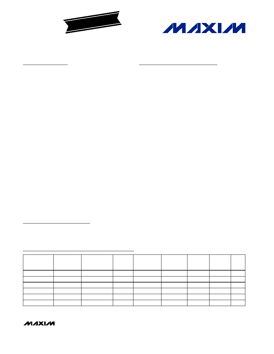
Ordering Information/Selector Guide
19-3280; Rev 2; 8/04
For pricing, delivery, and ordering information, please contact Maxim/Dallas Direct! at
1-888-629-4642, or visit Maxim's website at www.maxim-ic.com.
EVALUATION KIT
AVAILABLE
Pin Configurations appear at end of data sheet.
PART
TEMP RANGE
PIN-PACKAGE
REF
VOLTAGE
(V)
ANALOG
SUPPLY
VOLTAGE (V)
RESOLUTION
BITS***
ADC
CHANNELS
DAC
CHANNELS
GPIOs
MAX1020
BETX
-40
∞
C to +85
∞
C 36 Thin QFN-EP**
4.096
4.75 to 5.25
10
8
8
4
MAX1021
BETX* -40
∞
C to +85
∞
C 36 Thin QFN-EP**
2.5
2.7 to 3.6
10
8
8
4
MAX1022
BETX* -40
∞
C to +85
∞
C 36 Thin QFN-EP**
4.096
4.75 to 5.25
10
12
8
0
MAX1023
BETX* -40
∞
C to +85
∞
C 36 Thin QFN-EP**
2.5
2.7 to 3.6
10
12
8
0
MAX1057
BETM
-40
∞
C to +85
∞
C 48 Thin QFN-EP**
2.5
2.7 to 3.6
10
16
8
12
MAX1058
BETM
-40
∞
C to +85
∞
C 48 Thin QFN-EP**
4.096
4.75 to 5.25
10
16
8
12
SPI and QSPI are trademarks of Motorola, Inc.
MICROWIRE is a trademark of National Semiconductor Corp.
AutoShutdown is a trademark of Maxim Integrated Products, Inc.
*Future product--contact factory for availability.
**EP = Exposed pad.
***Number of resolution bits refers to both DAC and ADC.
MAX1020≠MAX1023/MAX1057/MAX1058
10-Bit, Multichannel ADCs/DACs with FIFO,
Temperature Sensing, and GPIO Ports
2
_______________________________________________________________________________________
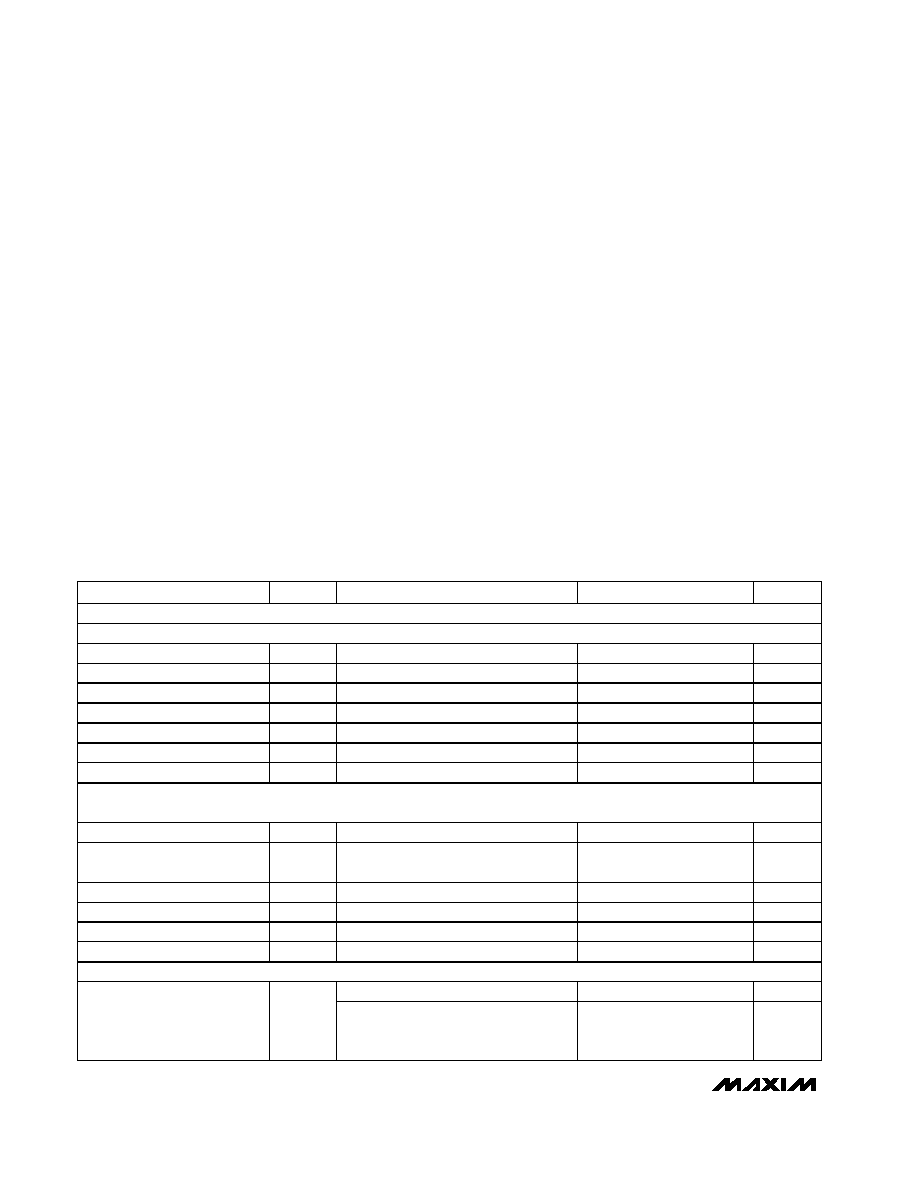
ABSOLUTE MAXIMUM RATINGS
ELECTRICAL CHARACTERISTICS
(AV
DD
= DV
DD
= 2.7V to 3.6V (MAX1021/MAX1023/MAX1057), external reference V
REF
= 2.5V (MAX1021/MAX1023/MAX1057), AV
DD
=
DV
DD
= 4.75V to 5.25V (MAX1020/MAX1022/MAX1058), external reference V
REF
= 4.096V (MAX1020/MAX1022/MAX1058), f
SCLK
= 4.8MHz
(50% duty cycle), T
A
= -40∞C to +85∞C, unless otherwise noted. Typical values are at AV
DD
= DV
DD
= 3V (MAX1021/MAX1023/MAX1057),
AV
DD
= DV
DD
= 5V (MAX1020/MAX1022/MAX1058), T
A
= +25∞C. Outputs are unloaded, unless otherwise noted.)
Stresses beyond those listed under "Absolute Maximum Ratings" may cause permanent damage to the device. These are stress ratings only, and functional
operation of the device at these or any other conditions beyond those indicated in the operational sections of the specifications is not implied. Exposure to
absolute maximum rating conditions for extended periods may affect device reliability.
AV
DD
to AGND .........................................................-0.3V to +6V
DGND to AGND.....................................................-0.3V to +0.3V
DV
DD
to AV
DD
.......................................................-3.0V to +0.3V
Digital Inputs to DGND.............................................-0.3V to +6V
Digital Outputs to DGND .........................-0.3V to (DV
DD
+ 0.3V)
Analog Inputs, Analog Outputs and REF_
to AGND ...............................................-0.3V to (AV
DD
+ 0.3V)
Maximum Current into Any Pin (except AGND, DGND, AV
DD
,
DV
DD
, and OUT_) ...........................................................50mA
Maximum Current into OUT_.............................................100mA
Continuous Power Dissipation (T
A
= +70∞C)
36-Pin Thin QFN (6mm x 6mm)
(derate 26.3mW/∞C above +70∞C) ......................2105.3mW
48-Pin Thin QFN (7mm x 7mm)
(derate 26.3mW/∞C above +70∞C) ......................2105.3mW
Operating Temperature Range ...........................-40∞C to +85∞C
Storage Temperature Range .............................-60∞C to +150∞C
Junction Temperature ......................................................+150∞C
Lead Temperature (soldering, 10s) .................................+300∞C
PARAMETER
SYMBOL
CONDITIONS
MIN
TYP
MAX
UNITS
ADC
DC ACCURACY
(Note 1)
Resolution
10
Bits
Integral Nonlinearity
INL
±0.5
±1.0
LSB
Differential Nonlinearity
DNL
±0.5
±1.0
LSB
Offset Error
±0.25
±2.0
LSB
Gain Error
(Note 2)
±0.025
±2.0
LSB
Gain Temperature Coefficient
±1.4
ppm/∞C
Channel-to-Channel Offset
±0.1
LSB
DYNAMIC SPECIFICATIONS (10kHz sine wave input, V
IN
= 2.5V
P-P
(MAX1021/MAX1023/MAX1057), V
IN
= 4.096V
P-P
(MAX1020/MAX1022/MAX1058), 300ksps, f
SCLK
= 4.8MHz)
Signal-to-Noise Plus Distortion
SINAD
61
dB
Total Harmonic Distortion
(Up to the Fifth Harmonic)
THD
-70
dBc
Spurious-Free Dynamic Range
SFDR
66
dBc
Intermodulation Distortion
IMD
f
in1
= 9.9kHz, f
in2
= 10.2kHz
72
dBc
Full-Linear Bandwidth
SINAD > 70dB
100
kHz
Full-Power Bandwidth
-3dB point
1
MHz
CONVERSION RATE
(Note 3)
External reference
0.8
µs
Power-Up Time
t
PU
Internal reference (Note 4)
218
C onver si on
C l ock
C ycl es
Note:
If the package power dissipation is not exceeded, one output at a time may be shorted to AV
DD
, DV
DD
, AGND, or DGND
indefinitely
MAX1020≠MAX1023/MAX1057/MAX1058
10-Bit, Multichannel ADCs/DACs with FIFO,
Temperature Sensing, and GPIO Ports
_______________________________________________________________________________________
3
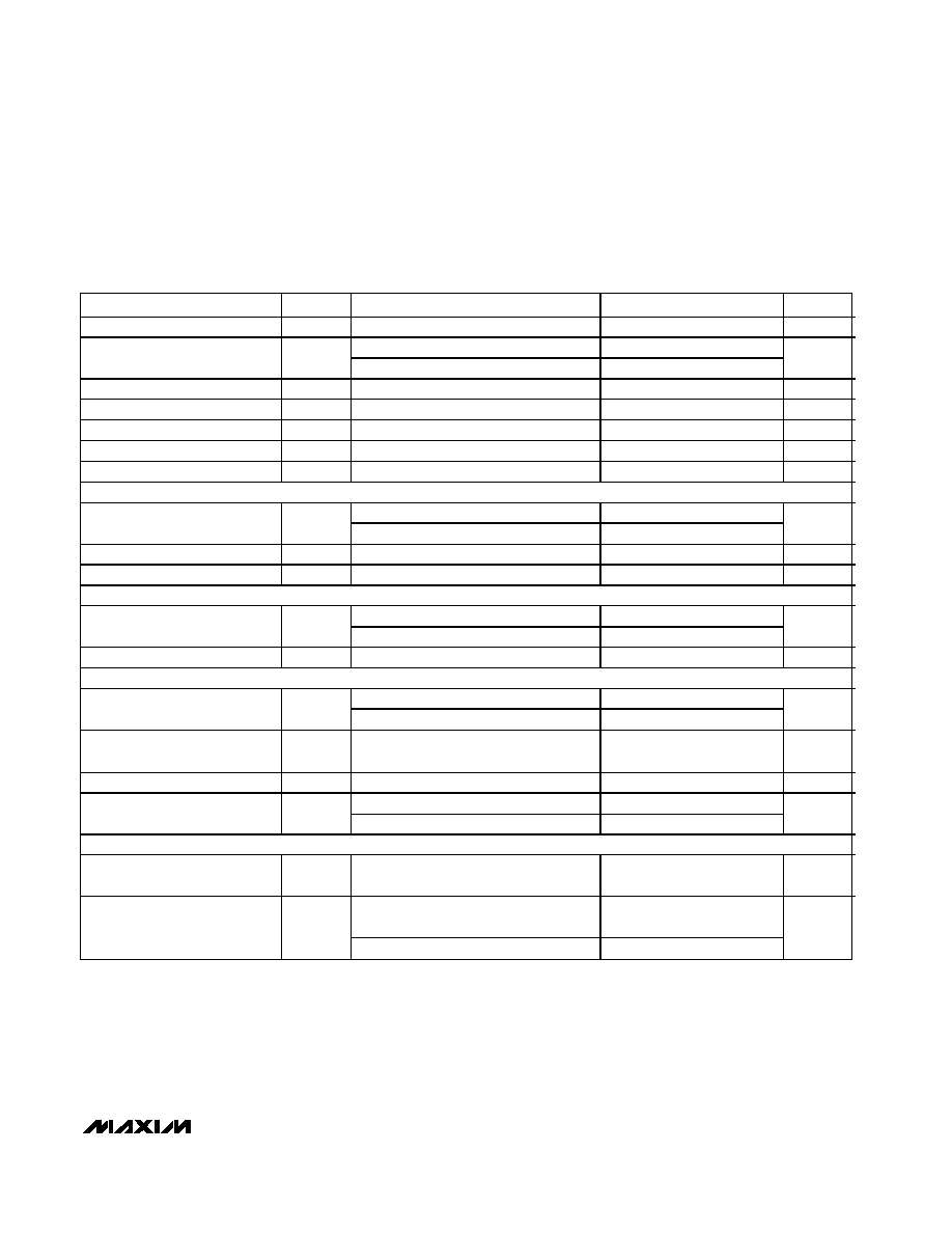
ELECTRICAL CHARACTERISTICS (continued)
(AV
DD
= DV
DD
= 2.7V to 3.6V (MAX1021/MAX1023/MAX1057), external reference V
REF
= 2.5V (MAX1021/MAX1023/MAX1057), AV
DD
=
DV
DD
= 4.75V to 5.25V (MAX1020/MAX1022/MAX1058), external reference V
REF
= 4.096V (MAX1020/MAX1022/MAX1058), f
SCLK
= 4.8MHz
(50% duty cycle), T
A
= -40∞C to +85∞C, unless otherwise noted. Typical values are at AV
DD
= DV
DD
= 3V (MAX1021/MAX1023/MAX1057),
AV
DD
= DV
DD
= 5V (MAX1020/MAX1022/MAX1058), T
A
= +25∞C. Outputs are unloaded, unless otherwise noted.)
PARAMETER
SYMBOL
CONDITIONS
MIN
TYP
MAX
UNITS
Acquisition Time
t
ACQ
(Note 5)
0.6
µs
Internally clocked
3.5
Conversion Time
t
CONV
Externally clocked
2.7
µs
Internal Clock Frequency
Internally clocked conversion
4.3
MHz
External Clock Frequency
f
CLK
Externally clocked conversion (Note 5)
0.1
4.8
MHz
Duty Cycle
40
60
%
Aperture Delay
30
ns
Aperture Jitter
<50
ps
ANALOG INPUTS
Unipolar
0
V
REF
Input Voltage Range (Note 6)
Bipolar
-V
REF
/ 2
V
REF
/ 2
V
Input Leakage Current
±0.01
±1
µA
Input Capacitance
24
pF
INTERNAL TEMPERATURE SENSOR
T
A
= +25∞C
±0.7
Measurement Error (Notes 5, 7)
T
A
= T
MIN
to T
MAX
±1.0
±3.0
∞C
Temperature Resolution
1/8
∞C/LSB
INTERNAL REFERENCE
MAX1021/MAX1023/MAX1057
2.482
2.50
2.518
REF1 Output Voltage (Note 8)
MAX1020/MAX1022/MAX1058
4.066
4.096
4.126
V
REF1 Voltage Temperature
Coefficient
TC
REF
±30
ppm/∞C
REF1 Output Impedance
6.5
k
V
REF
= 2.5V
0.39
REF1 Short-Circuit Current
V
REF
= 4.096V
0.63
mA
EXTERNAL REFERENCE
REF1 Input Voltage Range
V
REF1
REF mode 11 (Note 4)
1
AV
DD
+
0.05
V
REF mode 01
1
AV
DD
+
0.05
REF2 Input Voltage Range
(Note 4)
V
REF2
REF mode 11
0
1
V
MAX1020≠MAX1023/MAX1057/MAX1058
10-Bit, Multichannel ADCs/DACs with FIFO,
Temperature Sensing, and GPIO Ports
4
_______________________________________________________________________________________
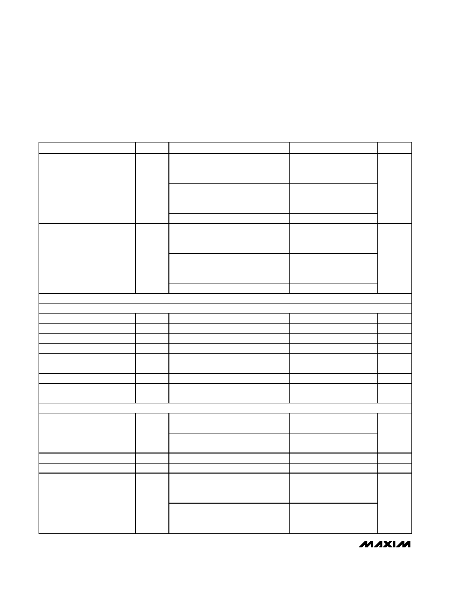
ELECTRICAL CHARACTERISTICS (continued)
(AV
DD
= DV
DD
= 2.7V to 3.6V (MAX1021/MAX1023/MAX1057), external reference V
REF
= 2.5V (MAX1021/MAX1023/MAX1057), AV
DD
=
DV
DD
= 4.75V to 5.25V (MAX1020/MAX1022/MAX1058), external reference V
REF
= 4.096V (MAX1020/MAX1022/MAX1058), f
SCLK
= 4.8MHz
(50% duty cycle), T
A
= -40∞C to +85∞C, unless otherwise noted. Typical values are at AV
DD
= DV
DD
= 3V (MAX1021/MAX1023/MAX1057),
AV
DD
= DV
DD
= 5V (MAX1020/MAX1022/MAX1058), T
A
= +25∞C. Outputs are unloaded, unless otherwise noted.)
PARAMETER
SYMBOL
CONDITIONS
MIN
TYP
MAX
UNITS
V
REF
= 2.5V
(MAX1021/MAX1023/MAX1057),
f
SAMPLE
= 300ksps
25
80
V
REF
= 4.096V
(MAX1020/MAX1022/MAX1058),
f
SAMPLE
= 300ksps
40
80
REF1 Input Current (Note 9)
I
REF1
Acquisition between conversions
±0.01
±1
µA
V
REF
= 2.5V
(MAX1021/MAX1023/MAX1057),
f
SAMPLE
= 300ksps
25
80
V
REF
= 4.096V
(MAX1020/MAX1022/MAX1058),
f
SAMPLE
= 300ksps
40
80
REF2 Input Current
I
REF2
Acquisition between conversions
±0.01
±1
µA
DAC
DC ACCURACY
(Note 10)
Resolution
10
Bits
Integral Nonlinearity
INL
±0.5
±1
LSB
Differential Nonlinearity
DNL
Guaranteed monotonic
±0.5
LSB
Offset Error
V
OS
(Note 8)
±3
±10
mV
Offset-Error Drift
±10
ppm of
FS/∞C
Gain Error
GE
(Note 8)
±1.25
±10
LSB
Gain Temperature Coefficient
±8
ppm of
FS/∞C
DAC OUTPUT
No load
0.02
AV
DD
-
0.02
Output-Voltage Range
10k
load to either rail
0.1
AV
DD
-
0.1
V
DC Output Impedance
0.5
Capacitive Load
(Note 11)
1
nF
AV
DD
= 2.7V, V
REF
= 2.5V
(MAX1021/MAX1023/MAX1057),
gain error < 1%
2000
Resistive Load to AGND
R
L
AV
DD
= 4.75V, V
REF
= 4.096V
(MAX1020/MAX1022/MAX1058),
gain error < 2%
500

MAX1020≠MAX1023/MAX1057/MAX1058
10-Bit, Multichannel ADCs/DACs with FIFO,
Temperature Sensing, and GPIO Ports
_______________________________________________________________________________________
5
ELECTRICAL CHARACTERISTICS (continued)
(AV
DD
= DV
DD
= 2.7V to 3.6V (MAX1021/MAX1023/MAX1057), external reference V
REF
= 2.5V (MAX1021/MAX1023/MAX1057), AV
DD
=
DV
DD
= 4.75V to 5.25V (MAX1020/MAX1022/MAX1058), external reference V
REF
= 4.096V (MAX1020/MAX1022/MAX1058), f
SCLK
= 4.8MHz
(50% duty cycle), T
A
= -40∞C to +85∞C, unless otherwise noted. Typical values are at AV
DD
= DV
DD
= 3V (MAX1021/MAX1023/MAX1057),
AV
DD
= DV
DD
= 5V (MAX1020/MAX1022/MAX1058), T
A
= +25∞C. Outputs are unloaded, unless otherwise noted.)
PARAMETER
SYMBOL
CONDITIONS
MIN
TYP
MAX
UNITS
From power-down mode, AV
DD
= 5V
25
Wake-Up Time (Note 12)
From power-down mode, AV
DD
= 2.7V
21
µs
1k
Output Termination
Programmed in power-down mode
1
k
100k
Output Termination
At wake-up or programmed in
power-down mode
100
k
DYNAMIC PERFORMANCE
(Notes 5, 13)
Output-Voltage Slew Rate
SR
Positive and negative
3
V/µs
Output-Voltage Settling Time
t
S
To 1 LSB, 400 - C00 hex (Note 7)
2
5
µs
Digital Feedthrough
Code 0, all digital inputs from 0 to DV
DD
0.5
nV
∑
s
Major Code Transition Glitch
Impulse
Between codes 2047 and 2048
4
nV
∑
s
From V
REF
660
Output Noise (0.1Hz to 50MHz)
Using internal reference
720
µV
P-P
From V
REF
260
Output Noise (0.1Hz to 500kHz)
Using internal reference
320
µV
P-P
DAC-to-DAC Transition
Crosstalk
0.5
nV
∑
s
INTERNAL REFERENCE
MAX1021/MAX1023/MAX1057
2.482
2.50
2.518
REF1 Output Voltage (Note 8)
MAX1020/MAX1022/MAX1058
4.066
4.096
4.126
V
REF1 Temperature Coefficient
TC
REF
±30
ppm/∞C
V
REF
= 2.5V
0.39
REF1 Short-Circuit Current
V
REF
= 4.096V
0.63
mA
EXTERNAL-REFERENCE INPUT
REF1 Input Voltage Range
V
REF1
REF modes 01, 10, and 11 (Note 4)
0.7
AV
DD
V
REF1 Input Impedance
R
REF1
70
100
130
k
DIGITAL INTERFACE
DIGITAL INPUTS (SCLK, DIN,
CS
,
CNVST
,
LDAC
)
Input-Voltage High
V
IH
DV
DD
= 2.7V to 5.25V
2.4
V
DV
DD
= 3.6V to 5.25V
0.8
Input-Voltage Low
V
IL
DV
DD
= 2.7V to 3.6V
0.6
V
Input Leakage Current
I
L
±0.01
±10
µA
Input Capacitance
C
IN
15
pF
DIGITAL OUTPUT (DOUT)
(Note 14)
Output-Voltage Low
V
OL
I
SINK
= 2mA
0.4
V