Äîêóìåíòàöèÿ è îïèñàíèÿ www.docs.chipfind.ru
General Description
The MAX1062 low-power, 14-bit analog-to-digital con-
verter (ADC) features a successive approximation ADC,
automatic power-down, fast 1.1µs wake-up, and a high-
speed SPITM/QSPITM/MICROWIRETM-compatible inter-
face. The MAX1062 operates with a single +5V analog
supply and features a separate digital supply, allowing
direct interfacing with 2.7V to 5.25V digital logic.
At the maximum sampling rate of 200ksps, the
MAX1062 consumes only 2.5mA. Power consumption is
only 12.5mW (AV
DD
= DV
DD
= 5V) at a 200ksps (max)
sampling rate. AutoShutdownTM reduces supply current
to 130µA at 10ksps and to less than 10µA at reduced
sampling rates.
Excellent dynamic performance and low power, com-
bined with ease of use and small package size (10-pin
µMAX) make the MAX1062 ideal for battery-powered
and data-acquisition applications or for other circuits
with demanding power consumption and space
requirements.
Applications
Motor Control
Industrial Process Control
Industrial I/O Modules
Data-Acquisition Systems
Thermocouple Measurements
Accelerometer Measurements
Portable- and Battery-Powered Equipment
Features
o 14-Bit Resolution, 1LSB DNL
o +5V Single-Supply Operation
o Adjustable Logic Level (2.7V to 5.25V)
o Input Voltage Range: 0 to V
REF
o Internal Track/Hold, 4MHz Input Bandwidth
o SPI/QSPI/MICROWIRE-Compatible Serial Interface
o Small 10-Pin µMAX Package
o Low Power
2.5mA at 200ksps
130µA at 10ksps
0.1µA in Power-Down Mode
MAX1062
14-Bit, +5V, 200ksps ADC with 10µA Shutdown
________________________________________________________________ Maxim Integrated Products
1
1
2
3
4
5
10
9
8
7
6
AIN
AGND
DV
DD
DGND
CS
AGND
AV
DD
REF
MAX1062
µMAX
TOP VIEW
DOUT
SCLK
Pin Configuration
Ordering Information
19-2203; Rev 0; 10/01
Functional Diagram appears at end of data sheet.
For pricing, delivery, and ordering information, please contact Maxim/Dallas Direct! at
1-888-629-4642, or visit Maxim's website at www.maxim-ic.com.
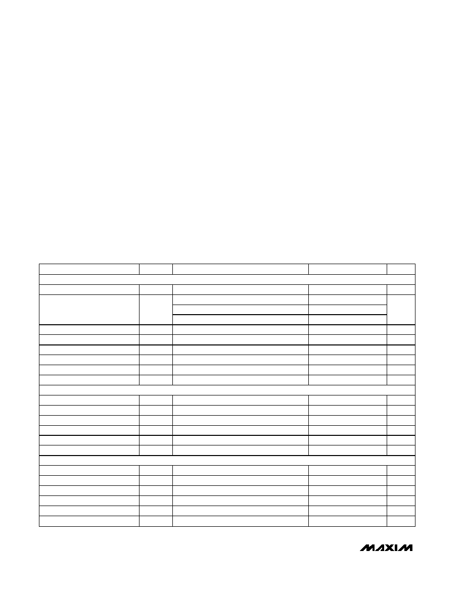
PART
TEMP.
RANGE
PIN-
PACKAGE
INL
(LSB)
MAX1062ACUB
0°C to 70
°C
10 µMAX
±1
MAX1062BCUB
0
°C to 70°C
10 µMAX
±2
MAX1062CCUB
0
°C to 70°C
10 µMAX
±3
MAX1062AEUB
-40
°C to 85°C
10 µMAX
±1
MAX1062BEUB
-40
°C to 85°C
10 µMAX
±2
MAX1062CEUB
-40
°C to 85°C
10 µMAX
±3
SPI and QSPI are trademarks of Motorola, Inc.
MICROWIRE is a trademark of National Semiconductor, Corp.
AutoShutdown is a trademark of Maxim Integrated Products, Inc.
MAX1062
14-Bit, +5V, 200ksps ADC with 10µA Shutdown
2
_______________________________________________________________________________________
ABSOLUTE MAXIMUM RATINGS
ELECTRICAL CHARACTERISTICS
(AV
DD
= DV
DD
= +4.75V to +5.25V, f
SCLK
= 4.8MHz (50% duty cycle), 24 clocks/conversion (200ksps), V
REF
= +4.096V, T
A
= T
MIN
to T
MAX
, unless otherwise noted. Typical values are at T
A
= +25°C.)
Stresses beyond those listed under "Absolute Maximum Ratings" may cause permanent damage to the device. These are stress ratings only, and functional
operation of the device at these or any other conditions beyond those indicated in the operational sections of the specifications is not implied. Exposure to
absolute maximum rating conditions for extended periods may affect device reliability.
AV
DD
to AGND ........................................................-0.3V to +6V
DV
DD
to DGND........................................................-0.3V to +6V
DGND to AGND....................................................-0.3V to +0.3V
AIN, REF to AGND ...................................-0.3V to (AV
DD
+ 0.3V)
SCLK, CS to DGND ..................................................-0.3V to +6V
DOUT to DGND .......................................-0.3V to (DV
DD
+ 0.3V)
Maximum Current Into Any Pin ...........................................50mA
Continuous Power Dissipation (T
A
= +70°C)
10-Pin µMAX (derate 5.6mW/°C above +70°C) ..........444mW
Operating Temperature Ranges
MAX1062_CUB .................................................0°C to +70°C
MAX1062_EUB ..............................................-40°C to +85°C
Maximum Junction Temperature .....................................+150°C
Storage Temperature Range .............................-65°C to +150°C
Lead Temperature (soldering, 10s) .................................+300°C
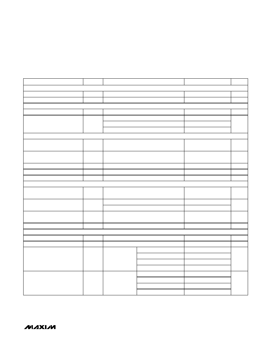
PARAMETER
SYMBOL
CONDITIONS
MIN
TYP
MAX
UNITS
DC ACCURACY (NOTE 1)
Resolution
14
Bits
MAX1062A
±1
MAX1062B
±2
Relative Accuracy (Note 2)
INL
MAX1062C
±3
LSB
Differential Nonlinearity
DNL
No missing codes over temperature
±0.5
±1
LSB
Transition Noise
RMS noise
±0.32
LSB
RMS
Offset Error
0.2
1
mV
Gain Error (Note 3)
±0.002
±0.01
%FSR
Offset Drift
0.4
ppm/
o
C
Gain Drift (Note 3)
0.2
ppm/
o
C
DYNAMIC SPECIFICATIONS (1kHz sine wave, 4.096Vp-p) (Note 1)
Signal-to-Noise Plus Distortion
SINAD
81
84
dB
Signal-to-Noise Ratio
SNR
82
84
dB
Total Harmonic Distortion
THD
-99
-86
dB
Spurious-Free Dynamic Range
SFDR
87
101
dB
Full-Power Bandwidth
-3dB point
4
MHz
Full-Linear Bandwidth
SINAD > 81dB
20
kHz
CONVERSION RATE
Conversion Time (Note 4)
t
CONV
5
240
µs
Serial Clock Frequency
f
SCLK
0.1
4.8
MHz
Aperture Delay
15
ns
Aperture Jitter
<50
ps
Sample Rate
f
S
f
SCLK
/ 24
200
ksps
Track/Hold Acquisition Time
t
ACQ
1.1
µs
MAX1062
14-Bit, +5V, 200ksps ADC with 10µA Shutdown
_______________________________________________________________________________________
3
ELECTRICAL CHARACTERISTICS (continued)
(AV
DD
= DV
DD
= +4.75V to +5.25V, f
SCLK
= 4.8MHz (50% duty cycle), 24 clocks/conversion (200ksps), V
REF
= +4.096V, T
A
= T
MIN
to T
MAX
, unless otherwise noted. Typical values are at T
A
= +25°C.)
PARAMETER
SYMBOL
CONDITIONS
MIN
TYP
MAX
UNITS
ANALOG INPUT (AIN)
Input Range
V
AIN
0
V
REF
V
Input Capacitance
C
AIN
40
pF
EXTERNAL REFERENCE
Input Voltage Range
V
REF
3.8
AV
DD
V
V
REF
= 4.096V, f
SCLK
= 4.8MHz
100
V
REF
= 4.096V, SCLK idle
0.01
Input Current
I
REF
CS = DV
DD
, SCLK idle
0.01
µA
DIGITAL INPUTS (SCLK, CS)
Input High Voltage
V
IH
DV
DD
= +2.7V to +5.25V
0.7 x
DV
DD
V
Input Low Voltage
V
IL
DV
DD
= +2.7V to +5.25V
0.3 x
DV
DD
V
Input Leakage Current
I
IN
V
IN
= 0 to DV
DD
±0.1
±1
µA
Input Hysteresis
V
HYST
0.2
V
Input Capacitance
C
IN
15
pF
DIGITAL OUTPUT (DOUT)
Output High Voltage
V
OH
I
SOURCE
= 0.5mA, DV
DD
= +2.7V to +5.25V
DV
DD
-
0.25V
V
I
SINK
= 10mA, DV
DD
= +4.75V to +5.25V
0.7
Output Low Voltage
V
OL
I
SINK
= 1.6mA, DV
DD
= +2.7V to +5.25V
0.4
V
Three-State Output Leakage
Current
I
L
CS = DV
DD
±0.1
±10
µA
Three-State Output Capacitance
C
OUT
CS = DV
DD
15
pF
POWER SUPPLIES
Analog Supply
AV
DD
4.75
5.25
V
Digital Supply
DV
DD
2.7
5.25
V
200ksps
2.0
2.5
100ksps
1.0
10ksps
0.1
Analog Supply Current
I
AVDD
CS = DGND
1ksps
0.01
mA
200ksps
0.6
1.0
100ksps
0.3
10ksps
0.03
Digital Supply Current
I
DVDD
CS = DGND,
DOUT = all
zeros
1ksps
0.003
mA
MAX1062
14-Bit, +5V, 200ksps ADC with 10µA Shutdown
4
_______________________________________________________________________________________
Note 1: AV
DD
= DV
DD
= +5V.
Note 2: Relative accuracy is the deviation of the analog value at any code from its theoretical value after the full-scale range has
been calibrated.
Note 3: Offset and reference errors nulled.
Note 4: Conversion time is defined as the number of clock cycles multiplied by the clock period; clock has 50% duty cycle.
Note 5: Defined as the change in positive full scale caused by a ±5% variation in the nominal supply voltage.
MAX1062 TIMING CHARACTERISTICS (Figures 1, 2, 3, and 6)
(AV
DD
= DV
DD
= +4.75V to +5.25V, f
SCLK
= 4.8MHz (50% duty cycle), 24 clocks/conversion (200ksps), V
REF
= +4.096V, T
A
= T
MIN
to T
MAX
, unless otherwise noted. Typical values are at T
A
= +25°C.)
PARAMETER
SYMBOL
CONDITIONS
MIN
TYP
MAX
UNITS
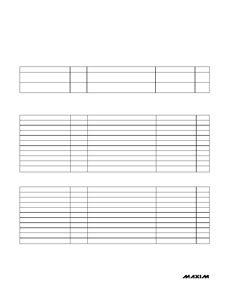
Acquisition Time
t
ACQ
1.1
µs
SCLK to DOUT Valid
t
DO
C
DOUT
= 50pF
50
ns
CS Fall to DOUT Enable
t
DV
C
DOUT
= 50pF
80
ns
CS Rise to DOUT Disable
t
TR
C
DOUT
= 50pF
80
ns
CS Pulse Width
t
CSW
50
ns
CS Fall to SCLK Rise Setup
t
CSS
100
ns
CS Rise to SCLK Rise Hold
t
CSH
0
ns
SCLK High Pulse Width
t
CH
65
ns
SCLK Low Pulse Width
t
CL
65
ns
SCLK Period
t
CP
208
ns
(AV
DD
= +4.75V to +5.25V, DV
DD
= +2.7V to +5.25V, f
SCLK
= 4.8MHz (50% duty cycle), 24 clocks/conversion (200ksps), V
REF
=
+4.096V, T
A
= T
MIN
to T
MAX
, unless otherwise noted. Typical values are at T
A
= +25°C.)
PARAMETER
SYMBOL
CONDITIONS
MIN
TYP
MAX
UNITS
Acquisition Time
t
ACQ
1.1
µs
SCLK to DOUT Valid
t
DO
C
DOUT
= 50pF
100
ns
CS Fall to DOUT Enable
t
DV
C
DOUT
= 50pF
100
ns
CS Rise to DOUT Disable
t
TR
C
DOUT
= 50pF
80
ns
CS Pulse Width
t
CSW
50
ns
CS Fall to SCLK Rise Setup
t
CSS
100
ns
CS Rise to SCLK Rise Hold
t
CSH
0
ns
SCLK High Pulse Width
t
CH
65
ns
SCLK Low Pulse Width
t
CL
65
ns
SCLK Period
t
CP
208
ns
ELECTRICAL CHARACTERISTICS (continued)
(AV
DD
= DV
DD
= +4.75V to +5.25V, f
SCLK
= 4.8MHz (50% duty cycle), 24 clocks/conversion (200ksps), V
REF
= +4.096V, T
A
= T
MIN
to T
MAX
, unless otherwise noted. Typical values are at T
A
= +25°C.)
PARAMETER
SYMBOL
CONDITIONS
MIN
TYP
MAX
UNITS
Shutdown Supply Current
I
AVDD
+
I
DVDD
CS = DV
DD
, SCLK = idle
0.1
10
µA
Power-Supply Rejection Ratio
(Note 5)
PSRR
AV
DD
= DV
DD
= +4.75V to +5.25V, full-scale
input
68
dB
MAX1062
14-Bit, +5V, 200ksps ADC with 10µA Shutdown
_______________________________________________________________________________________
5
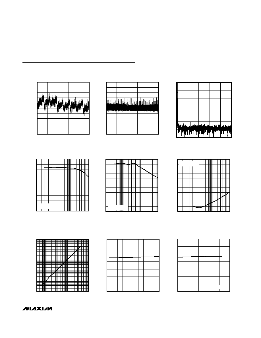
INL vs. OUTPUT CODE
MAX1062 toc01
OUTPUT CODE
INL (LSB)
13107
9830
6553
3276
-0.8
-0.6
-0.4
-0.2
0
0.2
0.4
0.6
0.8
1.0
-1.0
0
16384
DNL vs. OUTPUT CODE
MAX1062 toc02
OUTPUT CODE
DNL (LSB)
13107
9830
6553
3276
-0.8
-0.6
-0.4
-0.2
0
0.2
0.4
0.6
0.8
1.0
-1.0
0
16384
-140
-100
-120
-60
-80
-20
-40
0
0
40
20
60
80
10
50
30
70
90 100
MAX1062 FFT
MAX1062 toc03
FREQUENCY (kHz)
MAGNITUDE (dB)
90
0
0.1
100
10
1
SINAD
VS.
FREQUENCY
30
10
70
50
100
40
20
80
60
MAX1062 toc04
FREQUENCY (kHz)
SINAD (dB)
f
SAMPLE
= 200kHz
110
0
10
SFDR
VS.
FREQUENCY
MAX1062 toc05
FREQUENCY (kHz)
SFDR (dB)
20
30
40
50
60
70
80
90
100
0.1
100
10
1
f
SAMPLE
= 200kHz
0
-110
-100
THD
VS.
FREQUENCY
MAX1062 toc06
FREQUENCY (kHz)
THD (dB)
-90
-80
-70
-60
-50
-40
-30
-20
-10
0.1
100
10
1
f
SAMPLE
= 200kHz
10
0.01
0.1
1
10
100
1000
1
0.1
0.01
0.001
0.0001
SUPPLY CURRENT
VS.
CONVERSION RATE
MAX1062 toc07
CONVERSION RATE (kHz)
SUPPLY CURRENT (mA)
0
1.0
0.5
2.0
1.5
3.0
2.5
3.5
4.75
4.95
4.85
5.05
5.15
5.25
SUPPLY CURRENT
VS.
SUPPLY VOLTAGE
MAX1062 toc08
SUPPLY VOLTAGE (V)
SUPPLY CURRENT (mA)
0
1.0
0.5
2.0
1.5
3.0
2.5
3.5
-40
10
-15
35
60
85
SUPPLY CURRENT
VS.
TEMPERATURE
MAX1062 toc09
TEMPERATURE (
°C)
SUPPLY CURRENT (mA)
AV
DD
= DV
DD
= +5V
Typical Operating Characteristics
(AV
DD
= DV
DD
= +5V, f
SCLK
= 4.8MHz, C
LOAD
= 50pF, V
REF
= +4.096V, T
A
= 25°C, unless otherwise noted.)