
MAX1069
58.6ksps, 14-Bit, 2-Wire Serial ADC
in a 14-Pin TSSOP
________________________________________________________________ Maxim Integrated Products
1
19-2652; Rev 0; 10/02
For pricing, delivery, and ordering information, please contact Maxim/Dallas Direct! at
1-888-629-4642, or visit Maxim's website at www.maxim-ic.com.
General Description
The MAX1069 is a low-power, 14-bit successive-
approximation analog-to-digital converter (ADC). The
device features automatic power-down, an on-chip
4MHz clock, a +4.096V internal reference, and an
I
2
CTM-compatible 2-wire serial interface capable of both
fast and high-speed modes.
The MAX1069 operates from a single supply and con-
sumes 5mW at the maximum conversion rate of
58.6ksps. AutoShutdownTM powers down the device
between conversions, reducing supply current to less
than 50µA at a 1ksps throughput rate. The option of a
separate digital supply voltage allows direct interfacing
with +2.7V to +5.5V digital logic.
The MAX1069 performs a unipolar conversion on its
single analog input using its internal 4MHz clock. The
full-scale analog input range is determined by the inter-
nal reference or by an externally applied reference volt-
age ranging from 1V to AV
DD
.
The four address select inputs (ADD0≠ADD3) allow up
to sixteen MAX1069 devices on the same bus.
The MAX1069 is packaged in a 14-pin TSSOP and
offers both commercial and extended temperature
ranges. Refer to the MAX1169 for a 16-bit device in a
pin-compatible package.
Applications
Hand-Held Portable Applications
Medical Instruments
Battery-Powered Test Equipment
Solar-Powered Remote Systems
Receive Signal Strength Indicators
System Supervision
Features
o High-Speed I
2
C-Compatible Serial Interface
400kHz Fast Mode
1.7MHz High-Speed Mode
o +4.75V to +5.25V Single Supply
o +2.7V to +5.5V Adjustable Logic Level
o Internal +4.096V Reference
o External Reference: 1V to AV
DD
o Internal 4MHz Conversion Clock
o 58.6ksps Sampling Rate
o AutoShutdown Between Conversions
o Low Power
5.0mW at 58.6ksps
4.2mW at 50ksps
2.0mW at 10ksps
0.23mW at 1ksps
3µW in Shutdown
o Small 14-Pin TSSOP Package
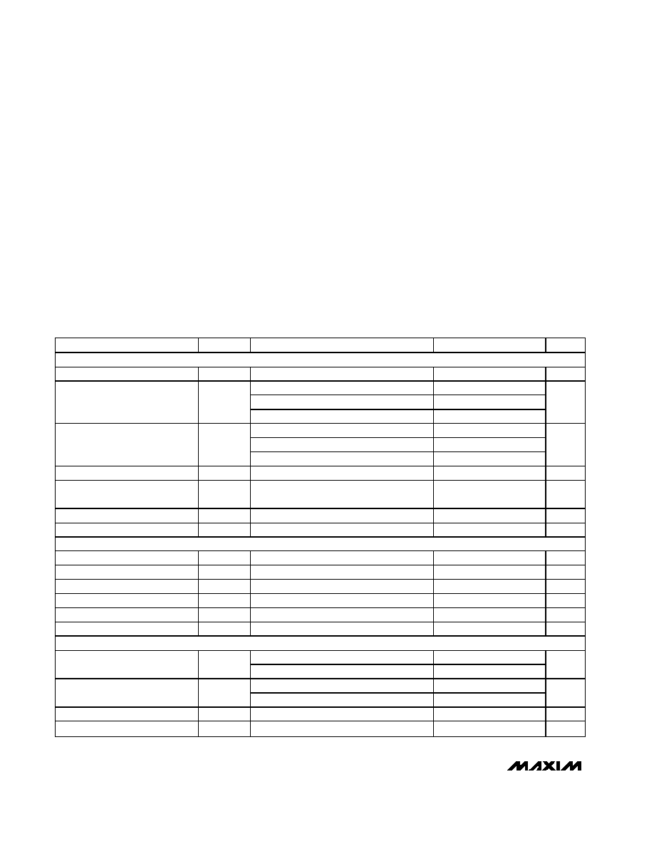
Ordering Information
PART
TEMP RANGE
PIN-
PACKAGE
INL
(LSB)
MAX1069ACUD
0∞C to +70∞C
14 TSSOP
±
1
MAX1069BCUD
0∞C to +70∞C
14 TSSOP
±
2
MAX1069CCUD
0∞C to +70∞C
14 TSSOP
±
3
MAX1069AEUD*
-40∞C to +85∞C
14 TSSOP
±
1
MAX1069BEUD*
-40∞C to +85∞C
14 TSSOP
±
2
MAX1069CEUD*
-40∞C to +85∞C
14 TSSOP
±
3
14
13
12
11
10
9
8
1
2
3
4
5
6
7
ADD3
REF
REFADJ
AGNDS
ADD2
SDA
SCL
DGND
TOP VIEW
MAX1069
AIN
AGND
AV
DD
DV
DD
ADD0
ADD1
TSSOP
Pin Configuration
I
2
C is a trademark of Philips Corp.
AutoShutdown is a trademark of Maxim Integrated Products, Inc.
*Future product--contact factory for availability.
MAX1069
58.6ksps, 14-Bit, 2-Wire Serial ADC
in a 14-Pin TSSOP
2
_______________________________________________________________________________________
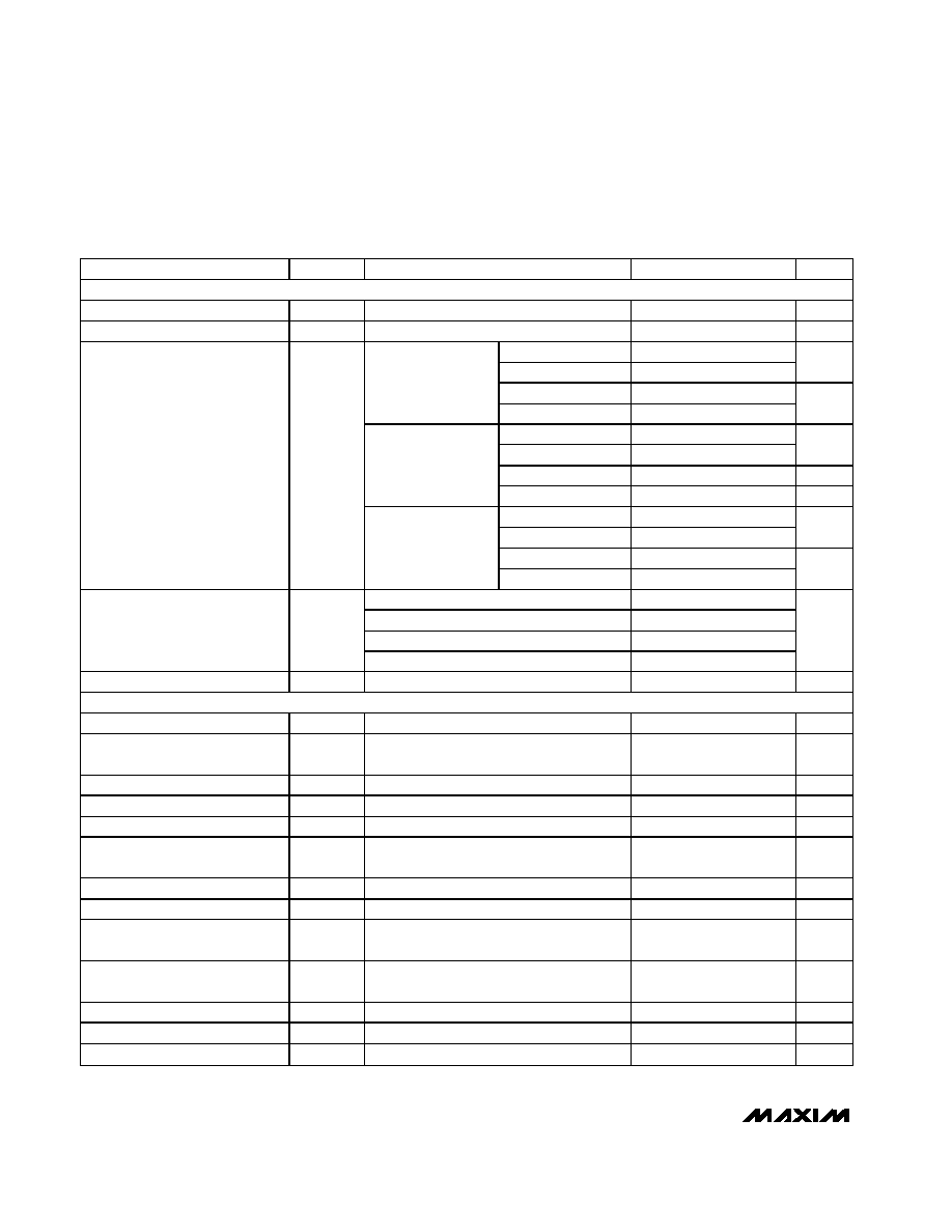
ABSOLUTE MAXIMUM RATINGS
Stresses beyond those listed under "Absolute Maximum Ratings" may cause permanent damage to the device. These are stress ratings only, and functional
operation of the device at these or any other conditions beyond those indicated in the operational sections of the specifications is not implied. Exposure to
absolute maximum rating conditions for extended periods may affect device reliability.
AV
DD
to AGND .........................................................-0.3V to +6V
DV
DD
to DGND .........................................................-0.3V to +6V
AGND to DGND.....................................................-0.3V to +0.3V
AGNDS to AGND...................................................-0.3V to +0.3V
AIN, REF, REFADJ to AGND....................-0.3V to (AV
DD
+ 0.3V)
SCL, SDA, ADD_ to DGND.......................................-0.3V to +6V
Maximum Current into Any Pin............................................50mA
Continuous Power Dissipation (T
A
= +70∞C)
14-Pin TSSOP (derate 9.1mW/∞C above +70∞C) .........727mW
Operating Temperature Ranges:
MAX1069_CUD ..................................................0∞C to +70∞C
MAX1069_EUD ................................................-40∞C to +85∞C
Storage Temperature Range .............................-65∞C to +150∞C
Junction Temperature ......................................................+150∞C
Lead Temperature (soldering, 10s) .................................+300∞C
ELECTRICAL CHARACTERISTICS
(AV
DD
= +4.75V to +5.25V, DV
DD
= +2.7V to +5.5V, f
SCL
= 1.7MHz (33% duty cycle), f
SAMPLE
= 58.6ksps, V
REF
= +4.096V, external ref-
erence applied to REF, REFADJ = AV
DD
, C
REF
= 10µF, T
A
= T
MIN
to T
MAX
, unless otherwise noted. Typical values are at T
A
= +25∞C.)
PARAMETER
SYMBOL
CONDITIONS
MIN
TYP
MAX
UNITS
DC ACCURACY (Note 1)
Resolution
14
Bits
MAX1069A
±1
MAX1069B
±2
Relative Accuracy
(Note 2)
INL
MAX1069C
±3
LSB
MAX1069A, no missing codes
±1
MAX1069B, no missing codes
±1
Differential Nonlinearity
DNL
MAX1069C, no missing codes
±1
LSB
Offset Error
2
5
mV
Offset-Error Temperature
Coefficient
1.0
ppm/
∞C
Gain Error
(Note 3)
±0.25
±0.5
%FSR
Gain Temperature Coefficient
0.1
ppm/
∞C
DYNAMIC PERFORMANCE (f
IN(sine wave)
= 1kHz, V
IN
= V
REF(P-P)
, f
SAMPLE
= 58.6ksps)
Signal-to-Noise Plus Distortion
SINAD
81
84
dB
Total Harmonic Distortion
THD
Up to the 5th harmonic
-99
-86
dB
Spurious-Free Dynamic Range
SFDR
87
102
dB
Signal-to-Noise Ratio
SNR
82
84
dB
Full-Power Bandwidth
FPBW
-3dB point
4
MHz
Full-Linear Bandwidth
SINAD > 81dB
20
kHz
CONVERSION RATE (Figure 11)
Fast mode
7.1
7.5
Conversion Time
(SCL Stretched Low)
t
CONV
High-speed mode
5.8
6
µs
Fast mode
19
Throughput Rate (Note 4)
f
SAMPLE
High-speed mode
58.6
ksps
Internal Clock Frequency
f
CLK
4
MHz
Track/Hold Acquisition Time
t
ACQ
(Note 5)
1100
ns

MAX1069
58.6ksps, 14-Bit, 2-Wire Serial ADC
in a 14-Pin TSSOP
_______________________________________________________________________________________
3
ELECTRICAL CHARACTERISTICS (continued)
(AV
DD
= +4.75V to +5.25V, DV
DD
= +2.7V to +5.5V, f
SCL
= 1.7MHz (33% duty cycle), f
SAMPLE
= 58.6ksps, V
REF
= +4.096V, external ref-
erence applied to REF, REFADJ = AV
DD
, C
REF
= 10µF, T
A
= T
MIN
to T
MAX
, unless otherwise noted. Typical values are at T
A
= +25∞C.)
PARAMETER
SYMBOL
CONDITIONS
MIN
TYP
MAX
UNITS
Fast mode
50
Aperture Delay
(Figure 11c) (Note 6)
t
AD
High-speed mode
30
ns
Fast mode
100
Aperture Jitter
(Figure 11c)
t
AJ
High-speed mode
100
ps
ANALOG INPUT (AIN)
Input Voltage Range
V
AIN
0
V
REF
V
Input Leakage Current
On/off-leakage current, V
AIN
= 0V or AV
DD
,
no clock, f
SCL
= 0
±0.01
±10
µA
Input Capacitance
C
IN
35
pF
INTERNAL REFERENCE (Bypass REFADJ with 0.1µF to AGND and REF with 10µF to AGND)
REF Output Voltage
V
REF
4.056
4.096
4.136
V
T
A
= 0∞C to +70∞C
±20
Reference Temperature
Coefficient
TC
REF
T
A
= -40∞C to +85∞C
±35
ppm/
∞C
Reference Short-Circuit Current
I
REFSC
10
4.136
mA
REFADJ Output Voltage
4.056
4.096
4.000
V
REFADJ Input Range
For small adjustments, from 4.096V
±60
mV
EXTERNAL REFERENCE (REFADJ = AV
DD
)
REFADJ Buffer Disable Voltage
Pull REFADJ high to disable the internal
bandgap reference and reference buffer
AV
DD
- 0.1
V
REFADJ Buffer Enable Voltage
AV
DD
- 0.4
V
Reference Input Voltage Range
(Note 7)
1.0
AV
DD
V
V
REF
= +4.096V, V
IN
= V
REF(P-P)
f
IN(sine wave)
= 1kHz, f
SAMPLE
= 62.1ksps
27
REF Input Current
I
REF
V
REF
= +4.096V, shutdown
0.1
µA
DIGITAL INPUTS/OUTPUTS (SCL, SDA)
Input High Voltage
V
IH
0.7
◊ DV
DD
V
Input Low Voltage
V
IL
0.3
◊ DV
DD
V
Input Hysteresis
V
HYST
0.1
◊ DV
DD
V
Input Current
I
IN
±10
µA
Input Capacitance
C
IN
15
pF
Output Low Voltage
V
OL
I
SINK
= 3mA
0.4
V
ADDRESS SELECT INPUTS (ADD3, ADD2, ADD1, ADD0)
Input High Voltage
0.7
◊ DV
DD
V
Input Low Voltage
0.3
◊ DV
DD
V
Input Hysteresis
0.1
◊ DV
DD
V
Input Current
±10
µA
Input Capacitance
15
pF
MAX1069
58.6ksps, 14-Bit, 2-Wire Serial ADC
in a 14-Pin TSSOP
4
_______________________________________________________________________________________
ELECTRICAL CHARACTERISTICS (continued)
(AV
DD
= +4.75V to +5.25V, DV
DD
= +2.7V to +5.5V, f
SCL
= 1.7MHz (33% duty cycle), f
SAMPLE
= 58.6ksps, V
REF
= +4.096V, external ref-
erence applied to REF, REFADJ = AV
DD
, C
REF
= 10µF, T
A
= T
MIN
to T
MAX
, unless otherwise noted. Typical values are at T
A
= +25∞C.)
PARAMETER
SYM B O L CONDITIONS
MIN
TYP
MAX
UNITS
POWER REQUIREMENTS (AV
DD
, AGND, DV
DD
, DGND)
Analog Supply Voltage
AV
DD
4.75
5.25
V
Digital Supply Voltage
DV
DD
2.7
5.5
V
f
SAMPLE
= 58.6ksps
1.8
2.5
f
SAMPLE
= 10ksps
0.7
mA
f
SAMPLE
= 1ksps
40
Inter nal r efer ence
( p ow er ed d ow n
b etw een conver si ons,
R/W = 0)
Shutdown
0.4
5.0
µA
f
SAMPLE
= 58.6ksps
1.8
2.5
f
SAMPLE
= 10ksps
1.4
mA
f
SAMPLE
= 1ksps
1.1
mA
Internal reference
(always on, R/W = 1)
Shutdown
0.4
5
µA
f
SAMPLE
= 58.6ksps
0.90
1.8
f
SAMPLE
= 10ksps
0.36
mA
f
SAMPLE
= 1ksps
40
Analog Supply Current
I
AVDD
External reference
(REFADJ = AV
DD
)
Shutdown
0.4
5
µA
f
SAMPLE
= 58.6ksps
260
400
f
SAMPLE
= 10ksps
65
f
SAMPLE
= 1ksps
6
Digital Supply Current
I
DVDD
Shutdown
0.2
5
µA
Power-Supply Rejection Ratio
PSRR
AV
DD
= 5V ±5%, full-scale input (Note 8)
2
6
LSB/V
TIMING CHARACTERISTICS FOR 2-WIRE FAST MODE (Figure 1a and Figure 2)
Serial Clock Frequency
f
SCL
400
kHz
Bus Free Time Between a STOP
and a START Condition
t
BUF
1.3
µs
Hold Time for Start Condition
t
HD,STA
0.6
µs
Low Period of the SCL Clock
t
LOW
1.3
µs
High Period of the SCL Clock
t
HIGH
0.6
µs
Setup Time for a Repeated
START Condition (Sr)
t
SU,STA
0.6
µs
Data Hold Time
t
HD,DAT
(Note 9)
0
900
ns
Data Setup Time
t
SU,DAT
100
ns
Rise Time of Both SDA and SCL
Signals, Receiving
t
R
(Note 10)
20 +
0.1C
B
300
ns
Fall Time of SDA Transmitting
t
F
(Note 10)
20 +
0.1C
B
300
ns
Setup Time for STOP Condition
t
SU,STO
0.6
µs
C ap aci ti ve Load for E ach Bus Li ne
C
B
400
pF
Pulse Width of Spike Suppressed
t
SP
50
ns
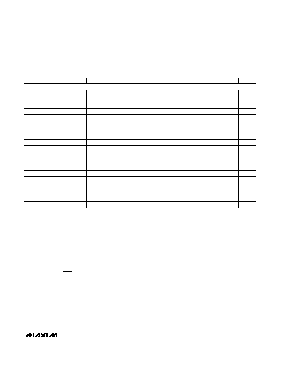
MAX1069
58.6ksps, 14-Bit, 2-Wire Serial ADC
in a 14-Pin TSSOP
_______________________________________________________________________________________
5
Note 1: DC accuracy is tested at AV
DD
= +5.0V and DV
DD
= +3.0V. Performance at power-supply tolerance limits is guaranteed
by power-supply rejection test.
Note 2: Relative accuracy is the deviation of the analog value at any code from its theoretical value after the full-scale range and
offset have been calibrated.
Note 3: Offset nullified.
Note 4: One sample is achieved every 18 clocks in continuous conversion mode.
Note 5: The track/hold acquisition time is two SCL cycles as illustrated in Figure 11.
Note 6: A filter on SDA and SCL delays the sampling instant and suppresses noise spikes less than 10ns in high-speed mode and
50ns in fast mode.
Note 7: ADC performance is limited by the converter's noise floor, typically 480µV
P-P
.
Note 8:
PSRR
V
(5.25V) - V
(4.75V)
2
V
5.25V - 4.75V
FS
FS
N
REF
=
[
]
◊
where N is the number of bits (
).
14
t
2
1
f
ACQ
SCL
= ◊
f
1 clocks
f
t
SAMPLE
SCL
C
-1
=
+
8
ONV
ELECTRICAL CHARACTERISTICS (continued)
(AV
DD
= +4.75V to +5.25V, DV
DD
= +2.7V to +5.5V, f
SCL
= 1.7MHz (33% duty cycle), f
SAMPLE
= 58.6ksps, V
REF
= +4.096V, external ref-
erence applied to REF, REFADJ = AV
DD
, C
REF
= 10µF, T
A
= T
MIN
to T
MAX
, unless otherwise noted. Typical values are at T
A
= +25∞C.)
PARAMETER
SYM B O L CONDITIONS
MIN
TYP
MAX
UNITS
TIMING CHARACTERISTICS FOR 2-WIRE HIGH-SPEED MODE (Figure 1b and Figure 2)
Serial Clock Frequency
f
SCLH
(Note 11)
1.7
MHz
Hold Time, (Repeated) Start
Condition
t
HD,STA
160
ns
Low Period of the SCL Clock
t
LOW
320
ns
High Period of the SCL Clock
t
HIGH
120
ns
Setup Time for a Repeated
START Condition
t
SU,STA
160
ns
Data Hold Time
t
HD,DAT
(Note 9)
0
150
ns
Data Setup Time
t
SU,DAT
10
ns
Rise Time of SCL Signal
(Current Source Enabled)
t
RCL
(Note 10)
10
80
ns
Rise Time of SCL Signal After
Acknowledge Bit
t
RCL1
(Note 10)
20
160
ns
Fall Time of SCL Signal
t
FCL
(Note 10)
20
80
ns
Rise Time of SDA Signal
t
RDA
(Note 10)
20
160
ns
Fall Time of SDA Signal
t
FDA
(Note 10)
20
160
ns
Setup Time for STOP Condition
t
SU,STO
160
ns
C ap aci ti ve Load for E ach Bus Li ne
C
B
400
pF
Pulse Width of Spike Suppressed
t
SP
10
ns